EP0473440B1 - An optical wave-length filter and a driving method thereof - Google Patents
An optical wave-length filter and a driving method thereof Download PDFInfo
- Publication number
- EP0473440B1 EP0473440B1 EP91307934A EP91307934A EP0473440B1 EP 0473440 B1 EP0473440 B1 EP 0473440B1 EP 91307934 A EP91307934 A EP 91307934A EP 91307934 A EP91307934 A EP 91307934A EP 0473440 B1 EP0473440 B1 EP 0473440B1
- Authority
- EP
- European Patent Office
- Prior art keywords
- mode
- waveguide
- filter
- electrode means
- mode converter
- Prior art date
- Legal status (The legal status is an assumption and is not a legal conclusion. Google has not performed a legal analysis and makes no representation as to the accuracy of the status listed.)
- Expired - Lifetime
Links
Images


Classifications
-
- G—PHYSICS
- G02—OPTICS
- G02F—OPTICAL DEVICES OR ARRANGEMENTS FOR THE CONTROL OF LIGHT BY MODIFICATION OF THE OPTICAL PROPERTIES OF THE MEDIA OF THE ELEMENTS INVOLVED THEREIN; NON-LINEAR OPTICS; FREQUENCY-CHANGING OF LIGHT; OPTICAL LOGIC ELEMENTS; OPTICAL ANALOGUE/DIGITAL CONVERTERS
- G02F1/00—Devices or arrangements for the control of the intensity, colour, phase, polarisation or direction of light arriving from an independent light source, e.g. switching, gating or modulating; Non-linear optics
- G02F1/01—Devices or arrangements for the control of the intensity, colour, phase, polarisation or direction of light arriving from an independent light source, e.g. switching, gating or modulating; Non-linear optics for the control of the intensity, phase, polarisation or colour
- G02F1/03—Devices or arrangements for the control of the intensity, colour, phase, polarisation or direction of light arriving from an independent light source, e.g. switching, gating or modulating; Non-linear optics for the control of the intensity, phase, polarisation or colour based on ceramics or electro-optical crystals, e.g. exhibiting Pockels effect or Kerr effect
- G02F1/035—Devices or arrangements for the control of the intensity, colour, phase, polarisation or direction of light arriving from an independent light source, e.g. switching, gating or modulating; Non-linear optics for the control of the intensity, phase, polarisation or colour based on ceramics or electro-optical crystals, e.g. exhibiting Pockels effect or Kerr effect in an optical waveguide structure
- G02F1/0353—Devices or arrangements for the control of the intensity, colour, phase, polarisation or direction of light arriving from an independent light source, e.g. switching, gating or modulating; Non-linear optics for the control of the intensity, phase, polarisation or colour based on ceramics or electro-optical crystals, e.g. exhibiting Pockels effect or Kerr effect in an optical waveguide structure involving an electro-optic TE-TM mode conversion
-
- G—PHYSICS
- G02—OPTICS
- G02F—OPTICAL DEVICES OR ARRANGEMENTS FOR THE CONTROL OF LIGHT BY MODIFICATION OF THE OPTICAL PROPERTIES OF THE MEDIA OF THE ELEMENTS INVOLVED THEREIN; NON-LINEAR OPTICS; FREQUENCY-CHANGING OF LIGHT; OPTICAL LOGIC ELEMENTS; OPTICAL ANALOGUE/DIGITAL CONVERTERS
- G02F1/00—Devices or arrangements for the control of the intensity, colour, phase, polarisation or direction of light arriving from an independent light source, e.g. switching, gating or modulating; Non-linear optics
- G02F1/01—Devices or arrangements for the control of the intensity, colour, phase, polarisation or direction of light arriving from an independent light source, e.g. switching, gating or modulating; Non-linear optics for the control of the intensity, phase, polarisation or colour
- G02F1/0136—Devices or arrangements for the control of the intensity, colour, phase, polarisation or direction of light arriving from an independent light source, e.g. switching, gating or modulating; Non-linear optics for the control of the intensity, phase, polarisation or colour for the control of polarisation, e.g. state of polarisation [SOP] control, polarisation scrambling, TE-TM mode conversion or separation
- G02F1/0142—TE-TM mode conversion
-
- G—PHYSICS
- G02—OPTICS
- G02F—OPTICAL DEVICES OR ARRANGEMENTS FOR THE CONTROL OF LIGHT BY MODIFICATION OF THE OPTICAL PROPERTIES OF THE MEDIA OF THE ELEMENTS INVOLVED THEREIN; NON-LINEAR OPTICS; FREQUENCY-CHANGING OF LIGHT; OPTICAL LOGIC ELEMENTS; OPTICAL ANALOGUE/DIGITAL CONVERTERS
- G02F2201/00—Constructional arrangements not provided for in groups G02F1/00 - G02F7/00
- G02F2201/12—Constructional arrangements not provided for in groups G02F1/00 - G02F7/00 electrode
- G02F2201/124—Constructional arrangements not provided for in groups G02F1/00 - G02F7/00 electrode interdigital
-
- G—PHYSICS
- G02—OPTICS
- G02F—OPTICAL DEVICES OR ARRANGEMENTS FOR THE CONTROL OF LIGHT BY MODIFICATION OF THE OPTICAL PROPERTIES OF THE MEDIA OF THE ELEMENTS INVOLVED THEREIN; NON-LINEAR OPTICS; FREQUENCY-CHANGING OF LIGHT; OPTICAL LOGIC ELEMENTS; OPTICAL ANALOGUE/DIGITAL CONVERTERS
- G02F2203/00—Function characteristic
- G02F2203/05—Function characteristic wavelength dependent
- G02F2203/055—Function characteristic wavelength dependent wavelength filtering
Description
- The present invention relates to an optical wavelength selection filter which comprises a waveguide formed on a substrate; an input polarizer at an input to the waveguide, having a first polarization planer an output polarizer at an output of the waveguide, having a second different polarization plane; and a mode converter disposed along the waveguide between the polarizers for converting radiation from a first mode polarized in said first plane to a second mode polarized in said second plane, the mode converter comprising a multi-fingered reference electrode means interdigitated with a plurality of finger-like control electrode means. The present invention also relates to a method of tuning an optical wavelength selection filter.
- A known optical wavelength selection filter is disclosed in "Heisemann, F. et al., Electronics Letters, 23 (1987), 21st May, No. 11". However, the tuning range of the disclosed filter is only 8nm which is insufficient for practical application.
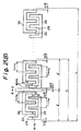
- Another filter structure is illustrated in Fig. 1. This structure has been proposed in order to provide an improvement in tuning range for optical filters.
- The optical wavelength filter illustrated in the Fig. 1 comprises a
waveguide path 12 formed in a substrate 10,polarizers output port 12b of thewaveguide path 12, and threemode converters 18 disposed between thepolarizers - In this filter, a
waveguide type polarizer 14 transmits TE mode light, awaveguide type polarizer 16 transmits TM mode light, and themode converters 18 convert TE mode light having a predetermined wavelength into TM mode light. - As a result, light having a predetermined wavelength can be selected from polychromatic light.
- The
mode converters 18 are configured such that the centre wavelengths λo of their bandwidths differ by ΔλT(max) from that of the adjacent mode converter(s) 18, where ΔλT(max) is the maximum tuning deviation of eachmode converter 18. - Each
mode converter 18 is constituted by a pair of interdigitated multi-fingered electrodes. Themulti-fingered electrodes 18a are located at predetermined locations along thewaveguide path 12. - The periods of the
multi-finger electrodes 18a of eachmode converter 18 differ from converter to converter. Consequently, the centre wavelengths λo of the mode converters differ from each other. - When a voltage V1 is applied to the
multi-finger electrodes 18a, in a similar manner to that used in a conventional filter, optical mode conversion can be performed on a predetermined wavelength. - The band width ΔλW of the of a mode converter can be described as;

type electrode 18a and the last finger-type electrode 18a ofmode converter 18. - Accordingly, in order to narrow the band width Δλw for improving filter characteristics, the length L of the mode converter must be increased.
- The conventional filter, however, necessitates a plurality of
mode converters 18 being coupled in series to select light having a predetermined wavelength. - As the result, there is the problem that the total length of the optical wavelength filter is required to be, at least, nL.
- A device related to that shown in Fig 1 is disclosed in US-A-4327971.
- "Izutsu, M et al, Optical Communications Conference; Amsterdam, 17-19 September 1979, pp 15.2-1 to 15.2-4" teaches that the conversion efficiency of a mode converter, as employed in the present invention, may be improved by applying a spatially, periodically varying control voltage to a split control electrode.
- It is aim of the present invention to provide a tunable optical filter having a practically useful tuning range without incurring the size penalty of the device of Fig. 1.
- According to the present invention, an optical wavelength selection filter includes controllable voltage generator means for applying a voltage pattern to the control electrode means, wherein the voltage pattern is or approximates a spatial sine wave and the voltage generator means is controllable to vary the period of said sine wave.
- Preferred features of a filter according to the present invention are set out in
claims 2 to 6. - The present invention also provides a method of tuning an optical wavelength selection filter which comprises a waveguide formed on a substrate; an input polarizer at an input to the waveguide, having a first polarization plane; an output polarizer at an output of the waveguide, having a second different polarization plane; and a mode converter disposed along the waveguide between the polarizers for converting radiation from a first mode polarized in said first plane to a second mode polarized in said second plane, the converter comprising a multi-fingered reference electrode means interdigitated with a plurality of finger-type control electrode means. A method according to the present invention comprises the steps of:
- (a) applying a first voltage pattern, which is or approximates a spatial sine wave having a first period, to the control electrode means, and
- (b) replacing the first voltage pattern with a second voltage pattern, which is or approximates a spatial sine wave having a second period, to the control electrode means, to thereby retune the filter.
- Embodiments of the present invention will now be described, by way of example, with reference to Figs. 2 to 10 of the accompanying drawings, in which:
- Fig. 1 is a perspective view illustrating one example of a conventional multi-stage optical wavelength filter;
- Figs. 2 (A) and (B) are explanatory views illustrating a first embodiment of the present invention;
- Figs. 3 (A) and (B) are explanatory views illustrating the operation of the first embodiment of the present invention;
- Fig. 4 is a wave form chart illustrating a smoothly alternating electric field distribution;
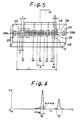
- Fig. 5 is a perspective view schematically illustrating a second embodiment of the present invention;
- Fig. 6 is an explanatory view of noise light;
- Figs. 7 (A) ~ (C) are explanatory views illustrating a third embodiment of the present invention;
- Figs. 8 (A) and (B) are explanatory views illustrating a fourth embodiment of the present invention;
- Figs. 9 (A) and (B) are wave form charts illustrating a voltage distribution and a transmitted wavelength band width M corresponding to the voltage distribution; and
- Figs. 10 (A) and (B) are wave form charts illustrating a voltage distribution and a transmitted wavelength bandwidth M corresponding to the voltage distribution.
- Referring to Figs. 2(A) and 2(B), an optical wavelength filter, according to the present invention, employs a
front stage polarizer 20 for transmitting input TM light, a plurality ofmode converter sections 22 for converting the input TM light, having a wavelength for which they are active, into TM light, and arear stage polarizer 24 for transmitting the TE light from themode converter sections 22 for output. Thepolarizers mode converter sections 22 are formed along awaveguide path 26. - The
mode converter sections 22 each comprise finger-type control electrodes 28 and finger-type earthing electrodes 30. The control andearthing electrodes waveguide path 26. - In this embodiment, the
waveguide path 26 is in the form of straight line and is formed by diffusing Ti in a X-cut LiNbO3 substrate 32. - The
front stage polarizer 20 is disposed at theinput port 26a of thewaveguide path 26 and therear stage polarizer 24 is disposed at theoutput port 26b. Thepolarizers - The finger-
type electrodes mode converter section 22 are coupled bycommon conductors 34,38 to form comb-shaped control and earthing electrode structures. - The period T of the
control electrodes 28 and the period t of theearthing electrodes 30 are equal to a period Λo (T = t = Λo) which is common to all of themode converter sections 22. - All of the
electrodes rear stage polarizers - The
lengths 1 of themode converter sections 22 are the same. - The
length 1 is defined as a distance between a position G/2 in the direction toward thefront stage polarizer 20 from the first electrode of amode converter section 22 and a position G/2 in the direction toward therear stage polarizer 24 from the last electrode of themode converter section 22. - The letter L, shown in Figs. 2 (A) and 2 (B), represents the overall length of the mode-conversion portion of an optical wavelength filter.
- Accordingly, if there are r
mode converter sections 22 between thepolarizers - The total length L corresponds to the length of a
single mode converter 18 employed in the optical wavelength filter shown in Fig. 1. - The "period" of the distribution of the
mode converter sections 22 is Λ1 which equals 2.l. - The letter W represents the width of an electrode and in this embodiment all the finger-
type electrodes - It is preferable to set the electrode width W to be equal to the electrode gap G (W = G).
- Each of parameters, set forth above, T, t, G, l, L, Λ1 and W is defined as a distance along the
waveguide path 26. - The control voltages applied to the
control electrodes 28 are such that the electric field distribution in thewaveguide path 26 approximates the product of two sine waves. - To simplify the voltage control for the
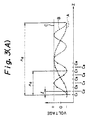
control electrodes 28, the same voltage Vm is applied to everyelectrode 28 belonging to the samemode converter section 22, where m is the mode converter index, the mode converter section nearest the input port having theindex 1, the next theindex 2 and so on. - Fig. 3 (A) shows a distribution of the voltage Vm in which the vertical axis represents voltage V and the horizontal axis represents a position z in a direction along the
waveguide path 26. - In the drawing, the letter Cm, representing the position of the m-th
mode converter section 22 along thewaveguide path 26, can mean either the starting, the ending or the centre position. - An appropriate position C1 is chosen on the z-axis and positions C2, C3, ..... are sequentially set from the position C1 with an interval l.
- The voltage Vm applied to the
control electrode 28 which belongs to the m-thmode converter section 22, located at the position Cm, is plotted as a black circle in the drawing. - The voltage Vm is set for driving the optical wavelength filter such that the distribution of the voltage Vm approximates a sine wave form as illustrated as black circles on curves A or B in Figure 3 (A).
- Preferably, the control voltage distribution is an accurate sine wave.
- However, this is not essential and an approximation of a sine wave may be used.
- The curves A and B are, for example, represented as V - sin z and the period of the curves A and B equals a period Λ2 described later (refer to Fig. 3 (B)).
- The voltage (= sin Cm) corresponding to the position Cm is, for example, represented by the voltage Vm.
- Since the same voltage Vm is applied to all the
control electrodes 28 of eachmode converter section 22, the voltage distribution is a step-wise approximation to a sine wave. - The curve A represents a distribution of the voltage Vm in the case of Λ1 < Λ2 < ∞, whereas the curve B represents in the case of Λ2 = Λ1.
- By way of the voltage Vm being applied to the
control electrodes 28 of the m-thmode converter section 22 and the earthingelectrodes 30 of all themode converter sections 22 being grounded to preserve the same potential, an approximately sine-wave distribution of electric field e(z) can be achieved in a direction along thewaveguide path 26. - The distribution of electric field e(z) achieved above is shown in Fig. 3 (B).
- In Fig. 3 (B), the vertical axis represents strength of electric field generated in the
waveguide path 26 in the direction of the thickness of a substrate and the horizontal axis represents the distance z along thewaveguide path 26. - As shown in Fig. 3 (B), the distribution of electric field e(z) is a step-wise approximation to the product of two sine waves.
- Although the distribution of electric field e(z) varies step-wise as described above, the distribution of electric field e(z) can be analogously considered to be a smoothly varying distribution of electric field E(z) when the
length 1 of themode converter section 22 is extremely small. - Fig. 4 shows the smoothly varying distribution of electric field E(z) and envelopes I and II thereof, in which the vertical axis represents strength of electric field in the
waveguide path 26 in the direction of the thickness of the substrate and the horizontal axis represents the distance z along thewaveguide path 26. - The smoothly varying distribution of electric field E(z) is described in general as follows:

- φ = 2·π/Λ0
- Δφ = 2·π/Λ2
- Λ2: period of envelope (refer to Fig. 3 (A))
- The second term (ei.Δφ.z ± e-i.Δφ.z) of the equation A represents the "modulation" of the distribution E(z); the "carrier" wave form of which approximates a sine-wave.
- The coupling equations of an optical wavelength filter in this case can be described as follows:


- a:
- amplitude in TM mode
- b:
- amplitude in TE mode
- K(z):
- coupling coefficient between the TM mode and the TE mode
- K*(z):
- complex conjugate of K(z)
- λ:
- wavelength of light
- Δn:
- difference of refractive index between TM mode and TE mode.
- Γ:
- effective coefficient
- n0:
- refractive index for normal light
- γ51:
- electro-optical coefficient of the substrate
- V:
- voltage applied to the control electrode
- G:
- electrode gap
- It is well known that at the wavelength λ, where the exponential term of K(z).ei.Δβ.z according to the equation (B) becomes zero notwithstanding the value of z, the coupling between TM and TE modes becomes effective to cause an inter-mode coupling.
- When Δβ < 0, the condition under which the phase term becomes zero notwithstanding the value of z is: Δβ = φ + Δφ or Δβ = φ - Δφ.
- The optical wavelength satisfying the equation Δβ = φ ± Δβ is described as follows:

- Light having the wavelength λ complying with the equation (E) is mode-converted and transmitted through the optical wavelength filter.
- Δn and Λ0 are predetermined structural design parameters and the optical wavelength λ transmitting through the optical wavelength filter can be varied by varying the period Λ2 of the voltage Vm.
- As readily understood in the equation (E), there are two kinds of the optical wavelength λ transmitting through the optical wavelength filter.
- The wavelength λ can be written as λ = λ0 + ΔλT, wherein λ0 is a standard design wavelength, and ΔλT is a deviation from the standard design wavelength λ0. Assuming ΔλTλ0(Λ0
 Λ2), in order to calculate the bandwidth of the filter, the following equation (F) is achieved from the equation (E):

- The following equation (G) is achieved by modification of the equation (F):

- The equation (G) clearly teaches that the optical wavelength filter can transmit light having the two wavelengths λ0 + ΔλT and λ0 - ΔλT.
- As readily understood from the analysis based upon the coupling equations as described above, when the smoothly varying distribution of electric field E(z) is generated, an optical wavelength filter can be achieved which is transmit light having two wavelengths λ0 + ΔλT and λ0 - ΔλT.
- By the way, when a distribution of electric field e(z) varying stepwise is generated, the coupling coefficient K(z) is described as follows:


- When j - 0, there arises a main peak of the light having the conversion wavelength corresponding to the band region M described later in Fig. 6 and when j ≠ 0, there arises a peak of the noise light corresponding to the band region N in Fig. 6.
- Around the peak,

- Accordingly, varying number of integral can be changed from dk to dδ.
- Assuming that fj(z) is an integral by dδ at each of the peak positions, K(z) is approximately described as follows:

- In the equation (I), the term f0(z) corresponds to the main peak of the light with a converted wavelength and equals the equation (D).
- The term fj(z) in case of j ≠ 0 corresponds to the peak of the noise light.
- In connection with the step-wise varying distribution of electric field e(z), above mentioned equations (E), (F) and (G) can not only be achieved but also the following (1) ∼ (3).
- (1): When Λ2 = Λ1 that is the repetition number of the period Λ2 becomes maximum, the maximum value ΔλT(max) of the deviation value ΔλT can be obtained, wherein the maximum value ΔλT (max) can be described as:

- (2): When the phase term equals to zero, since it does not differ from the case where Λ2 = ∞ (uniform mode-conversion, ΔλT = 0), the band width ΔλW in this embodiment where the optical wavelength filter transmits light having two wavelengths λ0 + ΔλT can be expressed as

- Accordingly, the band width ΔλW of the embodiment equals that shown in Fig. 1, assuming the lengths L of both elements are equal.
- The operational voltage of the optical wavelength filter according to the embodiment is approximately 1.5 times larger than that of the optical wavelength filter shown in Fig. 1.
- The channel number CH according to the embodiment is defined as CH = ΔλT(max) / ΔλW = L / Λ1 = periodic number N.
- When the total number of the
mode converter sections 22 is represented as Nmax which are disposed between thepolarizers - When the band width ΔλW and the channel number CH are respectively equal to each other in the embodiment and in Fig. 1, the total length of the optical wavelength filter shown in Fig. 1 needs to be n-times larger than that of the embodiment.
- (3): When the standard design wavelength λ0 is set as λ0 = 1.3 µm and a Ti-diffused waveguide route is formed in a LiNbO3 substrate, the band width ΔλW is described as ΔλW ≃ = 1.3 nm due to Λ0 ≃ 18 µm.
- Accordingly, Λ1 can be designed as Λ1 ≃ 180 µm in order to achieve the channel number CH being CH = 100, wherein the maximum deviation value ΔλT(max) is expressed as ΔλT(max) = 130 nm.
- A computer may be employed to control the voltages Vm applied to the
mode converter sections 22. - Hereinafter, only features differing from those of the first embodiment will be explained.
- A second embodiment of the invention is constituted such that the
length 1 of themode converter sections 22 becomes shorter (or longer) sequentially along a direction of arrangement. - The total numbers of the finger-
type electrodes mode converter sections 22 increase or decrease depending on the increase or decrease of the length L. - A
mode converter section 22 may contain one or more control and earthingelectrodes - One
mode converter section 22 constituted by a single finger-type electrode 28 for control and a single finger-type electrode 30 for earthing is shown in the drawing enclosed by the one-doted line indicated by the letter S. - Fig. 6 is an explanatory view of noise light, wherein the vertical axis represents conversion efficiency η of TM/TE mode conversion and the horizontal axis represents an optical wavelength λ.
- Fig. 6 shows the conversion efficiency η between the TM and TE modes wavelength λ for a filter according to the first embodiment of the present invention.
- As shown in the drawing, when an optical wavelength filter is driven, the mode-conversion of the light having a conversion wavelength (or an approximate conversion wavelength failing into the band width M having the band width Δλw from the central conversion wavelength) occurs and, in addition to that, the conversion efficiency η of the noise light (the light failing into the image wavelength band width N) is elevated to exceed -10dB at the peak value when the period Λ2 approaches to the period Λ1.
- However, since the length l of the
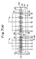
mode converter 22 of the second embodiment is set to be gradually shorter or longer sequentially, the conversion efficiency of the noise light can be reduced, whereby the peak value of the conversion efficiency of the noise light can be reduced to below -10dB even though the period Λ2 approaches to the period Λ1. - Figs. 7 (A) ∼ (C) are explanatory views of the embodiment according to the invention, wherein Fig. 7 (A) is a perspective view schematically illustrating the total construction of the third embodiment and Fig. 7 (B) is an enlarged plan view mainly illustrating the arrangement of the first mode converter, and Fig. 7 (C) is an enlarged plan view mainly illustrating the arrangement of a second mode converter.
- The elements corresponding to those of the above described embodiments are shown with the same numerals and detailed explanation will be omitted.
- An optical wavelength filter according to this embodiment employs, as shown in Fig. 7 (A), a
front stage polarizer 54 for transmitting input TM mode light, a plurality of the firstmode converter sections 56 for mode-converting input TM mode light, amiddle stage polarizer 58 for transmitting the TE mode light from thefirst mode converter 56, a plurality of the secondmode converter sections 60 for mode converting the TE mode light into TM mode light, and arear stage polarizer 62 for transmitting the TM mode light from thesecond mode converter 60 as output light, all of which are disposed along thewave guide path 26. - The first and the second
mode converter sections type electrodes 28 for control and finger-type electrodes 30 for earthing. - There are disposed, in the embodiment, a
front stage polarizer 54 located adjacent theinput port 26a of thewave guide path 26, arear stage polarizer 62 located adjacent theoutput port 26b, and amiddle stage polarizer 58 between thesepolarizers polarizers - The first element group I is formed such that a plurality of the first
mode converter sections 56 are disposed between thefront stage polarizer 54 and themiddle stage polarizer 58. - The second group II is formed such that a plurality of the second
mode converter sections 60 are disposed between themiddle stage polarizer 58 and therear stage polarizer 62. - The filter portion I, which has a similar construction to the first embodiment, is constituted by the
front stage polarizer 54, themiddle stage polarizer 58 and a plurality of the firstmode converter sections 56 between both these polarizers. - The filter portion II, which has a similar construction to the first embodiment, is constituted by the
middle stage polarizer 58, therear stage polarizer 62 and a plurality of the second-mode converter sections 60 between these polarizers. - The filter portion I inputs the TM mode light from the
input port 26a and converts the TM light having the conversion wavelength into TE mode light to be output. - The filter portion II converts the TE mode light having the conversion wavelength selectively among the input TE mode light from the filter portion I into TM mode light to be output from the
output port 26b. - This embodiment, as shown in Figs. 7 (B) and 7 (C), is constituted such that the period T1 of the
control electrodes 28 and the period t1 of the earthingelectrodes 30 employed in the firstmode converter sections 56 are respectively set to a common first period Λ01 (T1 = t1 = Λ01), and the period T2 of thecontrol electrodes 28 and the period t2 of the earthingelectrodes 30 employed in the secondmode converter sections 60 are respectively set to a common second period Λ02 (T2 = t2 = Λ02). - These periods Λ01 and Λ02 differ each other (Λ01 ≠ Λ02).
- The lengths l1 of all the first
mode converter sections 56 are set to be equal for each other and the lengths l2 of all the secondmode converter sections 60 are set to be equal to each other, wherein either l1 = l2 or l1 ≠ l2 is possible. - Further, all the finger-
type electrodes middle stage polarizers type electrodes rear stage polarizers - The letters L1 and L2 appearing in Figs. 7 (B) and 7 (C) represent the total lengths of the filter portions I and II, and Λ11 and Λ12 represent the distribution "period" of the first
mode converter sections 56 and the secondmode converter sections 60 in which Λ11 = 2.l1 and Λ12 = 2.l2, and Wl and W2 represent the electrode widths. - This embodiment is constituted such that the electrode widths of the finger-
type electrodes first mode converters 56 are commonly set to the electrode width W1 and the electrode width of the finger-type electrodes second mode converters 60 are commonly set to the electrode width W2. - The electrode gap G1 is preferably set to be equal to the electrode width W1 and the electrode gap G2 equal to the electrode width W2 in the same way.
- The voltage applied to each
control electrode 28 is controlled such that the distribution of electric field e1(z) along thewaveguide path 26 of the firstmode converter sections 56 and the distribution of electric field e2(z) along thewaveguide path 26 of the secondmode converter sections 60 are both approximations of the product of two sine waves. - In addition, the distributions of electric fields e1(z) and e2(z) are arranged such that mode conversion takes place in both filter portions I, II for light having the same free space wavelength.
- The distribution of electric field e1(z) is utilized for converting the TM mode light into the TE mode light in the filter portion I and the distribution of electric field e2(z) is utilized for converting the TE mode light into the TM mode light in the filter portion II.
- Further, in the embodiment the first voltage Vn applied to the
control electrodes 28 of the firstmode converter sections 56 is controlled in order to mode-convert the TM mode light into TE mode light. - In addition to that, the second voltage Un applied to the finger-
type electrodes 28 of each secondmode converter sections 60 is controlled in order to mode-convert the TE mode light into TM mode light. - The distribution of electric field e1(z) and the first voltage Vn in the filter portion I and the distribution of electric field e2(z) and the second voltage Un in the filter portion II are controlled in the manner described with reference to the first embodiment.
- The conversion wavelength of the first
mode converter sections 56 in the filter portion I is given as λ01 ± ΔλT1, wherein ΔλT1 varies in response to the variation of the period Λ22 of the second voltage Un. - In Fig. 8 (A) the horizontal axis represents the optical wavelength λ mode-converted in the filter portion I and the vertical axis represents the conversion efficiency η, and, in Fig. 8 (B), the horizontal axis represents the optical wavelength λ mode-converted in the filter portion II and the vertical axis represents the conversion efficiency η.
- When the first period Λ01 equals to the second period Λ02, that is, λ01 = λ02, the optical wavelength selected by the optical wavelength filter becomes λ0 ± ΔλT1 (= λ0 ± ΔλT2) notwithstanding the control of ΔλT1 and ΔλT2.
- However, when the first period Λ01 differs from the second period Λ02, that is, λ01 ≠ λ02, the optical wavelength can be varied by controlling ΔλT1 and ΔλT2, as is clear from Fig. 8.
- When λ01 + ΔλT1 = λ02 + ΔλT2, then λ01 - ΔλT1 ≠ λ02 - ΔλT2, or when λ01 - ΔλT1 = λ02 - ΔλT2, then λ01 + ΔλT1 ≠ λ02 + ΔλT2.
- When λ01 + ΔλT1 = λ02 + ΔλT2, then λ01 - ΔλT1 ≠ λ02 - ΔλT2 so that the optical wavelength selected by the optical wavelength filter becomes one single wavelength, that is, λ01 + ΔλT1 (= λ02 + ΔλT2).
- When λ01 - ΔλT1 = λ02 - ΔλT2, then λ01 + ΔλT1 ≠ λ02 + ΔλT2 so that the optical wavelength selected by the optical wavelength filter becomes one single wavelength, that is, λ01 - ΔλT1 ( = λ02 - ΔλT2).
- According to the embodiment, the channel number of the optical wavelength filter of the third embodiment is twice that of the first embodiment.
- This embodiment generates the first and the second distributions of electric field e1(z) and e2(z) concurrently and adjusts periods of both the first and the second voltages Vn and Un in such a manner that either of the two conversion wavelengths of filter portion I coincides with either of the two conversion wavelengths of the
second mode converter 60 in the filter portion II, whereby a light with a desired wavelength can be selected from polychromatic light. - The shape of the pass-band of a filter according to the present invention can be improved by setting the voltages, applied to the
control electrodes 28, such that the mode conversion efficiency at the ends of the filter is less than that at the centre of the filter. This will be now be explained with reference to Figs. 8 and 10. - Fig. 9 (A) illustrates a voltage Vm distribution applied to a filter according to the first embodiment of the present invention. The vertical axis is applied voltage (Vm) and the horizontal axis is displacement along the waveguide path (z).
- Fig. 9 (B) is a plot of conversion efficiency (η) against wavelength (λ) where Vm is as shown in Fig. 9 (A). M indicates the filters pass-band.
- Figs. 10 (A) and (B) are respectively plots of applied control voltage against displacement along the waveguide path and efficiency against wavelength in the case where the applied voltage Vm is arranged such that the mode conversion efficiency at the ends of the filter is less than that at the centre of the filter.
- As illustrated in Fig. 10 (A), when the voltage Vm is applied in such a manner that TM to TE mode-conversion efficiency of mode conversion at the end portions C1, C2, C6 and C7 is smaller than that at the centre portion C3, C4 and C5, the shape of the filter's pass-band approaches the desired rectangular form.
- The embodiments according to the present invention enable filters to be constructed with bandwidths of approximately 1 nm and which are tunable over a range greater than 100 nm.
- In the foregoing description, the spacing between adjacent electrode pairs R is equal to G. However, this is not essential and R could be set to an integer multiple of G.
Claims (7)
- An optical wavelength selection filter, comprising a waveguide (26) formed on a substrate (32); an input polarizer (20) at an input to the waveguide (26), having a first polarization plane; an output polarizer (24) at an output of the waveguide (26), having a second different polarization plane; and a mode converter (22) disposed along the waveguide (26) between the polarizers (20,24) for converting radiation from a first mode polarized in said first plane to a second mode polarized in said second plane, the converter (22) comprising a multi-fingered reference electrode means (36) interdigitated with a plurality of finger-type control electrode means (28), characterised by controllable voltage generator means for applying voltage pattern (A,B) to the control electrode means (28), wherein the voltage pattern (A,B) is or approximates a spatial sine wave and the voltage generator means is controllable to vary the period of said sine wave.
- A filter according to claim 1, wherein the spacing between the finger elements (28,30) of said electrode means is constant along the waveguide (26) between the polarizers (20,24).
- A filter according to claim 1 or 2, wherein groups of neigbouring control electrode means (28) are electrically coupled together so as to define a plurality of mode converter sections (22) distributed along the waveguide (26).
- A filter according the claim 3, wherein the periodicity of the finger elements (28,30) of the reference and control electrode means (36,34) is constant within each mode converter section (22).
- A filter according to claim 4, wherein the lengths of the mode converter sections (22) increase or decrease towards the output polarizer (24).
- A optical wavelength selection filter comprising two cascaded filters according to any preceding claim, wherein the output polarizer (58) of one filter acts as the input polarizer for the succeeding filter.
- A method of tuning an optical wavelength selection filter which comprises a waveguide (26) formed on a substrate (32); an input polarizer (20) at an input to the waveguide (26), having a first polarization plane; an output polarizer (24) at an output of the waveguide (26), having a second different polarization plane; and a mode converter (22) disposed along the waveguide (26) between the polarizers (20,24) for converting radiation from a first mode polarized in said first plane to a second mode polarized in said second plane, the converter (22) comprising a multi-fingered reference electrode means (36) interdigitated with a plurality of finger-like control electrode means (34), the method comprising the steps of:(a) applying a first voltage pattern (A,B), which is or approximates a spatial sine wave having a first period, to the control electrode means (34), and(b) replacing the first voltage pattern (A,B) with a second voltage pattern (A,B), which is or approximates a spatial sine wave having a second period, to the control electrode means (34), to thereby tune the filter.
Applications Claiming Priority (2)
| Application Number | Priority Date | Filing Date | Title |
|---|---|---|---|
| JP2228858A JP2902082B2 (en) | 1990-08-30 | 1990-08-30 | Optical wavelength filter and driving method thereof |
| JP228858/90 | 1990-08-30 |
Publications (3)
| Publication Number | Publication Date |
|---|---|
| EP0473440A2 EP0473440A2 (en) | 1992-03-04 |
| EP0473440A3 EP0473440A3 (en) | 1992-09-23 |
| EP0473440B1 true EP0473440B1 (en) | 1997-02-12 |
Family
ID=16882989
Family Applications (1)
| Application Number | Title | Priority Date | Filing Date |
|---|---|---|---|
| EP91307934A Expired - Lifetime EP0473440B1 (en) | 1990-08-30 | 1991-08-29 | An optical wave-length filter and a driving method thereof |
Country Status (4)
| Country | Link |
|---|---|
| US (1) | US5133028A (en) |
| EP (1) | EP0473440B1 (en) |
| JP (1) | JP2902082B2 (en) |
| DE (1) | DE69124649T2 (en) |
Families Citing this family (13)
| Publication number | Priority date | Publication date | Assignee | Title |
|---|---|---|---|---|
| GB9220430D0 (en) * | 1992-09-28 | 1992-11-11 | Marconi Gec Ltd | Optical filter |
| SE502139C2 (en) * | 1992-12-09 | 1995-08-28 | Ellemtel Utvecklings Ab | Electrically controllable filter device |
| US5446807A (en) * | 1994-06-23 | 1995-08-29 | Bell Communications Research, Inc. | Passband-flattened acousto-optic polarization converter |
| FR2752950B1 (en) * | 1996-09-02 | 1998-10-09 | Alsthom Cge Alcatel | BANDPASS FILTER INSERTED IN AN OPTICAL WAVEGUIDE |
| US5808528A (en) * | 1996-09-05 | 1998-09-15 | Digital Microwave Corporation | Broad-band tunable waveguide filter using etched septum discontinuities |
| US5889900A (en) * | 1997-05-16 | 1999-03-30 | Ramar Corporation | Integrated optic tunable filters and their methods of fabrication and use |
| CA2261197A1 (en) | 1999-02-16 | 2000-08-16 | Ppm Photomask Inc. | Tunable electro-optical diffraction grating with electrically switchable period |
| US7092419B2 (en) * | 2001-09-10 | 2006-08-15 | San Jose Systems, Inc. | Wavelength agile laser |
| JP2004163874A (en) * | 2002-05-28 | 2004-06-10 | Optun (Bvi) Ltd | Optical switching, and method and apparatus for variable optical attenuation |
| US7218814B2 (en) | 2002-05-28 | 2007-05-15 | Optun (Bvi) Ltd. | Method and apparatus for optical mode conversion |
| CN100505593C (en) * | 2004-07-21 | 2009-06-24 | 北京大学 | Polarization mould dispersion compensator |
| JP4542422B2 (en) | 2004-12-10 | 2010-09-15 | 富士通株式会社 | Optical device and drive voltage supply apparatus |
| JP2012163614A (en) * | 2011-02-03 | 2012-08-30 | Furukawa Electric Co Ltd:The | Soa-plc hybrid integrated circuit with polarization diversity and manufacturing method for the same |
Family Cites Families (7)
| Publication number | Priority date | Publication date | Assignee | Title |
|---|---|---|---|---|
| US4327971A (en) * | 1978-06-05 | 1982-05-04 | Nippon Electric Co., Ltd. | Electro-optical light modulators, light wavelength multiplex signal transmitting apparatus and light wavelength separating switches utilizing the same |
| US4359260A (en) * | 1980-06-25 | 1982-11-16 | Bell Telephone Laboratories, Incorporated | Optical polarizer |
| US4533207A (en) * | 1983-06-21 | 1985-08-06 | At&T Bell Laboratories | Wavelength tunable TE to TM mode converter |
| EP0260595B1 (en) * | 1986-09-18 | 1993-03-10 | Siemens Aktiengesellschaft | Device for continuous polarization and phase control without resetting |
| DE3874199T2 (en) * | 1987-05-01 | 1993-02-11 | Nec Corp | POLARIZATION CONTROL DEVICE. |
| US4966431A (en) * | 1989-08-10 | 1990-10-30 | At&T Bell Laboratories | Integrated-optic endless polarization transformer |
| US5002349A (en) * | 1989-11-29 | 1991-03-26 | Bell Communications Research, Inc. | Integrated acousto-optic filters and switches |
-
1990
- 1990-08-30 JP JP2228858A patent/JP2902082B2/en not_active Expired - Lifetime
-
1991
- 1991-08-29 DE DE69124649T patent/DE69124649T2/en not_active Expired - Fee Related
- 1991-08-29 EP EP91307934A patent/EP0473440B1/en not_active Expired - Lifetime
- 1991-08-29 US US07/752,080 patent/US5133028A/en not_active Expired - Lifetime
Also Published As
| Publication number | Publication date |
|---|---|
| EP0473440A2 (en) | 1992-03-04 |
| JP2902082B2 (en) | 1999-06-07 |
| DE69124649T2 (en) | 1997-09-04 |
| US5133028A (en) | 1992-07-21 |
| JPH04109216A (en) | 1992-04-10 |
| DE69124649D1 (en) | 1997-03-27 |
| EP0473440A3 (en) | 1992-09-23 |
Similar Documents
| Publication | Publication Date | Title |
|---|---|---|
| EP0473440B1 (en) | An optical wave-length filter and a driving method thereof | |
| US4146297A (en) | Tunable optical waveguide directional coupler filter | |
| US4448479A (en) | Traveling wave, electrooptic devices with effective velocity matching | |
| US4866406A (en) | Wide-band optical modulator | |
| Alferness | Guided-wave devices for optical communication | |
| EP0547779B1 (en) | Soliton generator | |
| US4127320A (en) | Multimode optical modulator/switch | |
| US4679893A (en) | High switching frequency optical waveguide switch, modulator, and filter devices | |
| US4533207A (en) | Wavelength tunable TE to TM mode converter | |
| US4288785A (en) | Light intensity modulator with digital control and a digital-analog converter comprising such a modulator | |
| US20050175271A1 (en) | Optical modulator | |
| US4273411A (en) | Optical wavelength filter | |
| US11733586B2 (en) | Integrated electro-optic frequency comb generator | |
| NL8201133A (en) | TUNABLE POLARIZATION-INDEPENDENT FILTER FOR OPTICAL WAVE LENGTHS. | |
| EP0239220A1 (en) | Electro-optic phase shifter with reduced input capacitance | |
| US5513283A (en) | Te-Me mode converter on polymer waveguide | |
| WO2000049457A1 (en) | Electrically adjustable diffraction grating | |
| US4843350A (en) | Coded sequence travelling-wave optical modulator | |
| US4832431A (en) | Apparatus for continuous polarization and phase control | |
| EP0425991B1 (en) | Waveguide-type optical switch | |
| EP0153312B1 (en) | Electro-optical filter device | |
| Bulmer et al. | Performance criteria and limitations of electrooptic waveguide array deflectors | |
| Jackel et al. | A passband-flattened acousto-optic filter | |
| EP0417295B1 (en) | Optical circuit element of waveguide type | |
| US6363189B1 (en) | Directional coupler |
Legal Events
| Date | Code | Title | Description |
|---|---|---|---|
| PUAI | Public reference made under article 153(3) epc to a published international application that has entered the european phase |
Free format text: ORIGINAL CODE: 0009012 |
|
| AK | Designated contracting states |
Kind code of ref document: A2 Designated state(s): DE FR GB |
|
| PUAL | Search report despatched |
Free format text: ORIGINAL CODE: 0009013 |
|
| AK | Designated contracting states |
Kind code of ref document: A3 Designated state(s): DE FR GB |
|
| 17P | Request for examination filed |
Effective date: 19930106 |
|
| 17Q | First examination report despatched |
Effective date: 19941216 |
|
| GRAG | Despatch of communication of intention to grant |
Free format text: ORIGINAL CODE: EPIDOS AGRA |
|
| GRAH | Despatch of communication of intention to grant a patent |
Free format text: ORIGINAL CODE: EPIDOS IGRA |
|
| GRAH | Despatch of communication of intention to grant a patent |
Free format text: ORIGINAL CODE: EPIDOS IGRA |
|
| GRAA | (expected) grant |
Free format text: ORIGINAL CODE: 0009210 |
|
| AK | Designated contracting states |
Kind code of ref document: B1 Designated state(s): DE FR GB |
|
| REF | Corresponds to: |
Ref document number: 69124649 Country of ref document: DE Date of ref document: 19970327 |
|
| ET | Fr: translation filed | ||
| PLBE | No opposition filed within time limit |
Free format text: ORIGINAL CODE: 0009261 |
|
| STAA | Information on the status of an ep patent application or granted ep patent |
Free format text: STATUS: NO OPPOSITION FILED WITHIN TIME LIMIT |
|
| 26N | No opposition filed | ||
| PGFP | Annual fee paid to national office [announced via postgrant information from national office to epo] |
Ref country code: FR Payment date: 20010810 Year of fee payment: 11 |
|
| PGFP | Annual fee paid to national office [announced via postgrant information from national office to epo] |
Ref country code: DE Payment date: 20010820 Year of fee payment: 11 |
|
| REG | Reference to a national code |
Ref country code: GB Ref legal event code: IF02 |
|
| PGFP | Annual fee paid to national office [announced via postgrant information from national office to epo] |
Ref country code: GB Payment date: 20020828 Year of fee payment: 12 |
|
| PG25 | Lapsed in a contracting state [announced via postgrant information from national office to epo] |
Ref country code: DE Free format text: LAPSE BECAUSE OF NON-PAYMENT OF DUE FEES Effective date: 20030301 |
|
| PG25 | Lapsed in a contracting state [announced via postgrant information from national office to epo] |
Ref country code: FR Free format text: LAPSE BECAUSE OF NON-PAYMENT OF DUE FEES Effective date: 20030430 |
|
| REG | Reference to a national code |
Ref country code: FR Ref legal event code: ST |
|
| PG25 | Lapsed in a contracting state [announced via postgrant information from national office to epo] |
Ref country code: GB Free format text: LAPSE BECAUSE OF NON-PAYMENT OF DUE FEES Effective date: 20030829 |
|
| GBPC | Gb: european patent ceased through non-payment of renewal fee |