EP0472161A1 - Pattern synchronizing circuit and method - Google Patents
Pattern synchronizing circuit and method Download PDFInfo
- Publication number
- EP0472161A1 EP0472161A1 EP91113932A EP91113932A EP0472161A1 EP 0472161 A1 EP0472161 A1 EP 0472161A1 EP 91113932 A EP91113932 A EP 91113932A EP 91113932 A EP91113932 A EP 91113932A EP 0472161 A1 EP0472161 A1 EP 0472161A1
- Authority
- EP
- European Patent Office
- Prior art keywords
- pattern
- input
- signal
- circuit
- reference pattern
- Prior art date
- Legal status (The legal status is an assumption and is not a legal conclusion. Google has not performed a legal analysis and makes no representation as to the accuracy of the status listed.)
- Withdrawn
Links
- 238000000034 method Methods 0.000 title claims description 6
- 230000001960 triggered effect Effects 0.000 claims abstract description 15
- 230000001360 synchronised effect Effects 0.000 claims description 5
- 230000003111 delayed effect Effects 0.000 claims description 3
- 230000008034 disappearance Effects 0.000 claims 7
- 230000001419 dependent effect Effects 0.000 abstract 1
- 238000010586 diagram Methods 0.000 description 3
- 238000006243 chemical reaction Methods 0.000 description 2
- 238000001514 detection method Methods 0.000 description 2
- 230000002401 inhibitory effect Effects 0.000 description 2
- 230000005540 biological transmission Effects 0.000 description 1
- 238000010276 construction Methods 0.000 description 1
- 238000012986 modification Methods 0.000 description 1
- 230000004048 modification Effects 0.000 description 1
Images

Classifications
-
- H—ELECTRICITY
- H04—ELECTRIC COMMUNICATION TECHNIQUE
- H04J—MULTIPLEX COMMUNICATION
- H04J3/00—Time-division multiplex systems
- H04J3/02—Details
- H04J3/06—Synchronising arrangements
- H04J3/0602—Systems characterised by the synchronising information used
- H04J3/0605—Special codes used as synchronising signal
- H04J3/0608—Detectors therefor, e.g. correlators, state machines
Landscapes
- Engineering & Computer Science (AREA)
- Computer Networks & Wireless Communication (AREA)
- Signal Processing (AREA)
- Synchronisation In Digital Transmission Systems (AREA)
- Detection And Prevention Of Errors In Transmission (AREA)
Abstract
An input pattern is re-timed in a re-timing circuit (15) by an input clock signal of the same frequency as that of the input pattern, and the re-timed input pattern and a reference pattern generated by a reference pattern generator (21) in synchronization with the input clock signal are compared by a digital error detector (18) to detect a mismatch between them. When the error rate dependent on the thus detected mismatch is larger than a predetermined value, an inhibit control circuit (26) inhibit one input clock pulse which is applied to the reference pattern generator, and when the error rate is smaller than the predetermined value, the inhibit control circuit generates a pattern synchronization establishment signal. When the pattern synchronization establishment signal disappears, a one-shot circuit (32) generates a pulse of a certain width, and if the pattern synchronization establishment signal is not generated again in this while, a T flip-flop (34) is triggered by the trailing edge of the pulse of the certain width. The output of the T flip-flop thus triggered is applied to an inverter (35), which inverts the polarity of the input pulse which is applied to the reference pattern generator and the re-timing circuit.
Description
- The present invention relates to a pattern synchronizing circuit and method for use with, for example, a digital error detector to produce from an input clock a reference pattern synchronized with an input pattern.
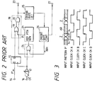
- In general, a digital error in the output of a certain apparatus or transmission line having input thereinto a code signal is detected in such a manner as shown in Fig. 1. A
test pattern generator 11 generates a test pattern P which repeats a bit pattern of a predetermined length, such as a pseudo-random binary sequence (PRBS) having a desired data bit cycle, and a test clock signal CK which rises substantially at the intermediate point of each data bit cycle of the test pattern P and has the same period as that of the data bit cycle. The test pattern P and the test clock signal CK are applied to a device undertest 12 and adigital error detector 13. An output pattern P' of the device undertest 12 is provided to thedigital error detector 13. The test pattern P of one period is, for example, 2²³-1 bits in length. In the digital error detector 13 a test pattern synchronized with the input pattern P' is produced, as a reference pattern Pr, based on the test clock signal CK, and the reference pattern Pr and the output pattern P' from the device undertest 12 are compared to detect a digital error in the latter. - Fig. 2 shows a conventional pattern synchronizing circuit for use in the
digital error detector 13 to create the reference pattern Pr synchronized with the input pattern P'. The input pattern P' from apattern input terminal 14 is applied to are-timing circuit 15, which is formed by a D flip-flop and in which the input pattern P' is re-timed by the input clock signal CK which is provided via avariable delay circuit 17 from aclock input terminal 16. The input pattern thus re-timed is applied to an exclusive-OR circuit 19 in a digitalerror detector circuit 18, wherein it is compared with the reference pattern Pr from areference pattern generator 21. The output of the exclusive-OR circuit 19 is applied to agate 22, which is supplied with the output clock of thevariable delay circuit 17. The exclusive-OR circuit 19 outputs a "1" or "0" , depending on whether or not the logical values of the both input patterns match each other. The output from the exclusive-OR circuit 19 is a NRZ waveform. In thegate 22 the NRZ waveform output is ANDed with the clock signal from thevariable delay circuit 17, by which it is converted to a RZ waveform. When the input pattern from there-timing circuit 15 does not match the reference pattern Pr, one pulse is output, as a digital error detected pulse, to aterminal 23 for each data bit cycle of the above-mentioned input pattern, and the detected pulse is applied to, for example, a high precision error rate detector (not shown). - The output clock signal of the
variable delay circuit 17 is provided via aninhibit gate 24 to thereference pattern generator 21, which produces the reference pattern Pr, based on the clock signal. When the reference pattern is not synchronized with the input pattern, many digital error detected pulses are produced. The digital error detected pulses are supplied to a simple-structurederror rate detector 25 which is formed by a frequency divider and by which the error rate is roughly measured. When the error rate is larger than 10⁻³, for instance, an inhibitgate control circuit 26 is caused to generate one inhibit pulse INH (which has a pulse width large enough to inhibit the input clock by one period), which is supplied to theinhibit gate 24, inhibiting the passage therethrough of one pulse of the input clock to delay the phase of the reference pattern Pr for one clock relative to the input pattern. Following this, the error rate is measured again and compared with the above-mentionedvalue 10⁻³, and if the former is larger than the latter, then another inhibit pulse INH is produced and the above-said operation is repeated. If the error rate is lower than 10 ⁻³, then no inhibit pulse INH is produced, but instead a pattern synchronization establishment signal is output via aterminal 27. This signal is used to indicate the establishment of synchronization of the input pattern with the reference pattern. The basic construction of such a conventional pattern synchronizing circuit is disclosed in U.S. Patent No.4,878,233, except re-timing of the input pattern. - As shown in Fig, 3, dead zones Z, which depend on the hold time th and the setup time ts of the D flip-flop forming the
re-timing circuit 15, exist before and after a data conversion node of the input pattern P' and when a jitter is present in the input pattern P', the dead zones Z become wider corresponding to the width of the jitter. In the case where the leading edge of the input clock CK which is supplied to there-timing circuit 15 is within the dead zone z as depicted in Fig. 3, Rows A,B and C, the output of there-timing circuit 15 does not become correct data and no output pattern is not established, but instead a pattern containing a large error (an error rate above 10⁻³, for example) is usually output. In this instance, no pattern synchronization establishment signal would be produced, even if it is repeated to delay the reference pattern Pr for one cycle by inhibiting the passage of the input clock CK through thegate 22 with the inhibit pulse INH. Now, let Lp, Tc and Td represent the length of the test pattern, the period of the input clock CK and the time until it is decided whether the error rate is higher or lower than 10⁻³ after the application of the inhibit pulse INH, respectively. In the case where no pattern synchronization is established even after the lapse of a maximum time necessary for the pattern synchronization, Ts = Lp × (Tc+Td), an operator adjusts thevariable delay circuit 17 to slightly delay the phase of the input clock CK from the state of Row A to the state of Row B in Fig.3, for example. Where the pattern synchronization is not established yet after the time Ts elapses again, the phase of the input clock CK is delayed to the state of Fig. 3C, and in the example of Fig. 3, the phase of the input clock CK is further delayed to the state of Row D in Fig. 3. Thus, the leading edge of the input clock signal CK enters a phase difference allowable range AR between the dead zones Z of the input pattern, and hence the pattern synchronization can be established. - As will be seen from the above, no effective means has been available for definitely judging that the leading edge of the input clock signal CK is in the dead zone z of the input pattern; therefore, the prior art repeats adjusting the variable delay circuit for each lapse of a fixed time--this is a cumbersome and time-consuming operation. This operation must be performed not only at the start of a test but also when the frequency of the input clock is changed during test and the leading edge of the input clock enters the dead zone of the input pattern.
- It is therefore an object of the present invention to provide a pattern synchronizing circuit and method which permit automatic synchronization of the reference pattern with the input pattern in a short time.
- With the pattern synchronizing circuit of the present invention, when the pattern synchronization establishment signal disappears, a one-shot circuit is triggered to generate a pulse of a time width larger than the maximum time Ts necessary for the establishment of synchronization. This pulse and the pattern synchronization establishment signal are applied to an OR circuit. In the asynchronous state a T flip-flop is triggered by the edge of the output of the OR circuit which is attributable to the trailing edge of the output pulse of the one-shot circuit. The output of the T flip-flop is supplied to an inverter, which inverts or does not invert the input clock signal to be supplied to the re-timing circuit, in accordance with the output of the T flip-flop.
- With the synchronizing method of the present invention, in the case where no synchronization is established within a predetermined period of time after the detection of a step out, the input clock signal is inverted by the inverter, after which no operation is involved until the pattern synchronization is established.
-
- Fig. 1 is a block diagram showing an ordinary digital error detection arrangement;
- Fig. 2 is a block diagram showing a conventional pattern synchronizing circuit;
- Fig. 3 is a graph showing the relationship between dead zones of an input pattern and an input clock signal;
- Fig. 4 is a block diagram illustrating an embodiment of the present invention;
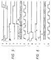
- Fig. 5 is a timing chart showing waveforms occurring at respective parts in Fig. 4, for explaining an operation in the case of inverting the polarity of the input clock signal; and
- Fig. 6 is a timing chart showing waveforms occurring at respective parts in Fig. 4, for explaining an operation in the case where the polarity of the input clock signal is not inverted.
- Fig. 4 illustrates in block form an embodiment of the present invention, in which the parts corresponding to those in Fig. 2 are identified by the same reference numerals. According to the present invention, the pattern synchronization establishment signal at the
terminal 27 also is provided via adelay circuit 28 to a NOR circuit serving as an OR gate, and at the same time, the pattern synchronization establishment signal is applied via anOR circuit 31 to a one-shot circuit 32. TheOR circuit 31 is supplied with a trigger pulse via aterminal 33 at the start of the apparatus. The one-shot circuit 32 is triggered when the pattern synchronization establishment signal enters the step-out state (i.e. goes low), or it is triggered by the trigger pulse at the start of the apparatus, and the one-shot circuit 32, thus triggered, outputs a pulse of a width T₀ larger than the sum of the afore-mentioned maximum time Ts necessary for the pattern synchronization and thedelay time τ ₀ of thedelay circuit 28. A T flip-flop 34 is triggered by the leading edge of the output from theNOR circuit 29 and the output of the T flip-flop 34 is applied as a control signal to aninverter 35 connected in series between theclock input terminal 16 and there-timing circuit 15. - With such an arrangement, when the pattern synchronization state is changed to the asynchronous state by, for example, a change in the frequency of the input clock signal and the pattern synchronization establishment signal goes low at a time point t₁ as shown on Row A in Fig. 5, the output of the
delay circuit 28 also goes low after the lapse oftime τ ₀ as shown on Row B in Fig. 5, and the one-shot circuit 32 is triggered by the trailing edge of the pattern synchronization establishment signal and yields the pulse of width T₀ as depicted on Row C in Fig. 5. In this state, if the leading edge of the input clock signal which is applied to there-timing circuit 15 is within the dead zone Z of the input pattern P' shown on Row F in Fig. 5, as depicted on Row G, no synchronization is not established even after the lapse of the maximum time Ts necessary for the pattern synchronization. However, after the elapsed time T₀ both inputs to theNOR circuit 29 go low and the output from theNOR circuit 29 goes high as shown on Row D in Fig. 5. The T flip-flop 34 is triggered by the leading edge of the output from theNOR circuit 29 and the flip-flop output goes high as depicted on Row E in Fig. 5. This high-level output is applied to an exclusive-OR circuit forming theinverter 35, by which the polarity of the input clock signal to be supplied to there-timing circuit 15 is inverted as shown on Row G in Fig. 5. Usually, the time length of the phase difference allowable range AR is larger than the time length of the dead zone Z, accordingly the leading edge of the inverted input clock signal is within the allowable range AR between adjacent data conversion nodes and correct re-timing takes place. As a result of this, synchronization is established at a certain time point, in this example, at a time point t₂ and the pattern synchronization establishment signal goes high as shown on Row A in Fig. 5. - In the case where the leading edge of the input clock signal is not within the dead zone Z of the input pattern as shown on Rows F and G when the reference pattern Pr goes out of step as depicted on Row A, the inhibit pulse INH is generated several times and synchronization is established at a time point t₃ before the lapse of time T₀ after the time point t₁ as shown on Row A and then the pattern synchronization establishment signal goes high. Accordingly, when the output of the one-
shot circuit 32 goes low as shown on Row C in Fig. 6, the output of theNOR circuit 29 remains low as depicted on Row D in Fig. 6 and the T flip-flop 34 will not be triggered. - At the start of the apparatus the pattern synchronization establishment signal is low from the beginning, but since the one-
shot circuit 32 is triggered by the trigger pulse from theterminal 33, the pattern synchronization is established within a time 2T₀. Incidentally, if thedelay circuit 28 is left out, there is a possibility that during the delay in the rise of the output pulse of the one-shot circuit 32 behind the rise of the pattern synchronization establishment signal A a whisker-like pulse is produced in the output of theNOR circuit 29 and the T flip-flop 34 is triggered by such a pulse. If there is no such a possibility fear, thedelay circuit 28 can be omitted. When thedelay circuit 28 is employed, thetime τ ₀ is selected to be longer than the delay time of the one-shot circuit 32. Thevariable delay circuit 17 may also be omitted by use of theinverter 35, but in the case where the input pattern contains many jitters, the relationship that the time of the dead zone is shorter than the time of the allowable range does not always hold, in which case adjustment by thevariable delay circuit 17 is required. - As described above, according to the present invention, even if the leading edge of the input clock signal is in the dead zone of the input pattern, the phase of the input clock signals automatically inverted after the lapse of time T₀, and consequently, synchronization is automatically established within a time slightly longer than twice the maximum time Ts necessary for synchronization and an operator need not perform any troublesome operations therefor.
- It will be apparent that many modifications and variations may be effected without departing from the scope of the novel concepts of the present invention.
Claims (9)
- A pattern synchronizing circuit comprising:
re-timing means supplied with an input pattern composed of a sequence of data and an input clock signal of the same frequency as that of said input pattern, for re-timing the former with the latter;
reference pattern generating means for generating a reference pattern for said input pattern in synchronization with said input clock signal;
digital error detecting means for comparing said reference pattern and said re-timed input pattern to detect a mismatch as a digital error;
error rate detecting means supplied with the detected output of said digital error detecting means, for detecting an error rate based on said detected output;
control means whereby it is checked whether or not said error rate is larger than a predetermined value, and if so, the passage of said input clock signal to be supplied to said reference pattern generating means is controlled to shift the phase of generation of said reference pattern in one direction, and if said error rate is smaller than said predetermined value, a pattern synchronization establishment signal is generated; and
clock inverting means which responds to disappearance of said pattern synchronization establishment signal to invert the polarity of said input clock signal to be applied to said reference pattern generating means and said re-timing means, if said pattern synchronization establishment signal is not generated within a predetermined period of time after the disappearance of said pattern synchronization establishment signal. - The pattern synchronizing circuit of claim 1, wherein said predetermined period of time is longer than the maximum time necessary for establishment of synchronization of said reference pattern generating means.
- The synchronizing circuit of claim 1, wherein said control means includes: a control circuit which outputs an inhibit pulse when said error rate is larger than said predetermined value and generates said pattern synchronization establishment signal when said error rate is smaller than said predetermined value; and inhibit gate means which normally permits the passage therethrough of said input clock signal to said reference pattern generating means but, when supplied with said inhibit pulse, inhibits the passage therethrough of one pulse of said input clock signal.
- The synchronizing circuit of claim 3, wherein said clock inverting means includes: means responsive to disappearance of said pattern synchronization establishment signal to generate an invert signal when said pattern synchronization establishment signal is not produced until said predetermined period of time elapses after the disappearance of said pattern synchronization establishment signal; and an inverter for inverting the polarity of said input clock signal by said invert signal for input into said inhibit gate means.
- The synchronizing circuit of claim 4, wherein said invert signal generating means includes: waiting time pulse generating means reponsive to the disappearance of said pattern synchronization establishment signal to generate a waiting time define pulse having a pulse width equal to said predetermined period of time; an OR circuit supplied with said waiting time define pulse and said pattern synchronization establishment signal, for outputting their OR; and flip-flop means which is triggered by the edge of the output of said OR circuit to generate said invert signal.
- A pattern synchronizing circuit wherein an input pattern is re-timed by an input clock signal of the same frequency as said input pattern in a re-timing circuit, a reference pattern for said input pattern is generated by a reference pattern generator in synchronization with said input clock signal a mismatch between said reference pattern and said re-timed input pattern is detected by a digital error detector, an error rate is detected by an error rate detector from the detected output, and when said detected error rate is larger than a predetermined value, the reference pattern generating phase of said reference pattern generator is shifted to synchronize said reference pattern with said input pattern, and when they are synchronized with each other, a pattern synchronization establishment signal is generated, the improvement comprising:
a one-shot circuit responsive to disappearance of said pattern synchronization establishment signal to generate a pulse of a time width larger than the maximum time necessary for establishment of synchronization of said reference pattern generator;
an OR circuit supplied with the output of said one-shot circuit and said pattern synchronization establishment signal;
a T flip-flop triggered by the edge of the output of said OR circuit; and
an inverter connected in series between the input terminal for said input clock signal and said re-timing circuit, for outputting said input clock signal after inverting it or without inverting it in accordance with the output of said T flip-flop. - The pattern synchronizing circuit of claim 5 or 6, further including delay means whereby said pattern synchronization establishment signal to be applied to said OR circuit is delayed for a predetermined period of time.
- A pattern synchronizing method comprising:
a step of re-timing an input pattern by an input clock signal of the same frequency as that of said input pattern;
a step of generating a reference pattern in synchronization with said input clock signal;
a step of detecting a mismatch between said reference pattern and said re-timed input pattern and obtaining an error rate from the detected output;
a step of checking whether or not said error rate is larger than a predetermined value and shifting the phase of generation of said reference pattern by a predetermined amount when said error rate is larger than said predetermined value;
a step of generating a pattern synchronization establishment signal when said error rate is smaller than said predetermined value; and
a step wherein disappearance of said pattern synchronization establishment signal is detected and, when said pattern synchronization establishment signal is not generated within a prefixed period of time thereafter, the polarity of said input clock signal is inverted to thereby delay the generation of said reference pattern and said re-timing by one clock. - The synchronizing method of claim 8, wherein said prefixed period of time is longer than the maximum time necessary for establishment of synchronization between said input pattern and said reference pattern.
Applications Claiming Priority (2)
| Application Number | Priority Date | Filing Date | Title |
|---|---|---|---|
| JP2220582A JPH04103240A (en) | 1990-08-22 | 1990-08-22 | Pattern synchronizing circuit |
| JP220582/90 | 1990-08-22 |
Publications (1)
| Publication Number | Publication Date |
|---|---|
| EP0472161A1 true EP0472161A1 (en) | 1992-02-26 |
Family
ID=16753233
Family Applications (1)
| Application Number | Title | Priority Date | Filing Date |
|---|---|---|---|
| EP91113932A Withdrawn EP0472161A1 (en) | 1990-08-22 | 1991-08-20 | Pattern synchronizing circuit and method |
Country Status (3)
| Country | Link |
|---|---|
| US (1) | US5163069A (en) |
| EP (1) | EP0472161A1 (en) |
| JP (1) | JPH04103240A (en) |
Cited By (2)
| Publication number | Priority date | Publication date | Assignee | Title |
|---|---|---|---|---|
| EP0611048A2 (en) * | 1993-01-28 | 1994-08-17 | AT&T Corp. | Method and arrangement for determining byte error rate |
| US5843565A (en) * | 1996-10-31 | 1998-12-01 | Ampex Corporation | Particulate magnetic medium utilizing keeper technology and methods of manufacture |
Families Citing this family (9)
| Publication number | Priority date | Publication date | Assignee | Title |
|---|---|---|---|---|
| US5430746A (en) * | 1992-06-09 | 1995-07-04 | Wandel & Goltermann Gmbh & Co. Elektronische Messtechnik | Method of and circuitry for detecting synchronism failure of two word sequences |
| US5444743A (en) * | 1993-11-18 | 1995-08-22 | Hitachi America, Ltd. | Synchronous pulse generator |
| JP2694807B2 (en) * | 1993-12-16 | 1997-12-24 | 日本電気株式会社 | Data transmission method |
| US5462220A (en) * | 1994-02-03 | 1995-10-31 | Advanced Container Corporation | Shipping and display box |
| US5661763A (en) * | 1995-07-28 | 1997-08-26 | Adtran, Inc. | Apparatus and method for detecting programmable length bit pattern in serial digital data stream |
| US5690272A (en) * | 1996-04-26 | 1997-11-25 | Universal Container, Inc. | Produce box |
| US6715094B2 (en) * | 2000-12-20 | 2004-03-30 | Intel Corporation | Mult-mode I/O interface for synchronizing selected control patterns into control clock domain to obtain interface control signals to be transmitted to I/O buffers |
| US6986091B2 (en) * | 2002-08-27 | 2006-01-10 | Agilent Technologies, Inc. | Method and apparatus for testing a high speed data receiver for jitter tolerance |
| US7412640B2 (en) * | 2003-08-28 | 2008-08-12 | International Business Machines Corporation | Self-synchronizing pseudorandom bit sequence checker |
Citations (3)
| Publication number | Priority date | Publication date | Assignee | Title |
|---|---|---|---|---|
| US4479230A (en) * | 1981-02-06 | 1984-10-23 | Lignes Telegraphiques & Telephoniques | Process and apparatus for the synchronization on reception of a signal provided with a synchronization pattern |
| EP0321837A2 (en) * | 1987-12-21 | 1989-06-28 | Advantest Corporation | Data pattern synchronizer |
| US4908871A (en) * | 1986-04-21 | 1990-03-13 | Hitachi, Ltd. | Pattern inspection system |
Family Cites Families (5)
| Publication number | Priority date | Publication date | Assignee | Title |
|---|---|---|---|---|
| US3824548A (en) * | 1973-01-15 | 1974-07-16 | Us Navy | Satellite communications link monitor |
| US4254492A (en) * | 1979-04-02 | 1981-03-03 | Rockwell International Corporation | Redundant clock system utilizing nonsynchronous oscillators |
| US4445116A (en) * | 1982-03-05 | 1984-04-24 | Burroughs Corporation | Method for allocating bandwidth between stations in a local area network |
| US4972442A (en) * | 1989-04-27 | 1990-11-20 | Northern Telecom Limited | Phase-locked loop clock |
| US5054035A (en) * | 1989-12-21 | 1991-10-01 | At&T Bell Laboratories | Digital signal quality evaluation circuit using synchronization patterns |
-
1990
- 1990-08-22 JP JP2220582A patent/JPH04103240A/en active Pending
-
1991
- 1991-08-20 EP EP91113932A patent/EP0472161A1/en not_active Withdrawn
- 1991-08-20 US US07/747,347 patent/US5163069A/en not_active Expired - Fee Related
Patent Citations (4)
| Publication number | Priority date | Publication date | Assignee | Title |
|---|---|---|---|---|
| US4479230A (en) * | 1981-02-06 | 1984-10-23 | Lignes Telegraphiques & Telephoniques | Process and apparatus for the synchronization on reception of a signal provided with a synchronization pattern |
| US4908871A (en) * | 1986-04-21 | 1990-03-13 | Hitachi, Ltd. | Pattern inspection system |
| EP0321837A2 (en) * | 1987-12-21 | 1989-06-28 | Advantest Corporation | Data pattern synchronizer |
| US4878233A (en) * | 1987-12-21 | 1989-10-31 | Advantest Corporation | Data pattern synchronizer |
Cited By (3)
| Publication number | Priority date | Publication date | Assignee | Title |
|---|---|---|---|---|
| EP0611048A2 (en) * | 1993-01-28 | 1994-08-17 | AT&T Corp. | Method and arrangement for determining byte error rate |
| EP0611048A3 (en) * | 1993-01-28 | 1995-04-12 | At & T Corp | Method and arrangement for determining byte error rate. |
| US5843565A (en) * | 1996-10-31 | 1998-12-01 | Ampex Corporation | Particulate magnetic medium utilizing keeper technology and methods of manufacture |
Also Published As
| Publication number | Publication date |
|---|---|
| JPH04103240A (en) | 1992-04-06 |
| US5163069A (en) | 1992-11-10 |
Similar Documents
| Publication | Publication Date | Title |
|---|---|---|
| US5761216A (en) | Bit error measurement system | |
| EP0472161A1 (en) | Pattern synchronizing circuit and method | |
| KR920004336B1 (en) | Synchronousness detection circuit | |
| US6636999B1 (en) | Clock adjusting method and circuit device | |
| US5210754A (en) | Pattern synchronizing circuit | |
| US4819251A (en) | High speed non-return-to-zero digital clock recovery apparatus | |
| US4964117A (en) | Timing synchronizing circuit for baseband data signals | |
| US4583221A (en) | Synchronization system for key telephone system | |
| US5367543A (en) | Circuit for detecting synchronizing signal in frame synchronization data transmission | |
| US4955040A (en) | Method and apparatus for generating a correction signal in a digital clock recovery device | |
| US4775989A (en) | Timing phase detector circuit | |
| KR20000006499A (en) | Timing signal generating apparatus and method | |
| EP0472160A2 (en) | High-rate pulse pattern generator | |
| KR910000624B1 (en) | Bit synchronous circuits and methods | |
| US5430746A (en) | Method of and circuitry for detecting synchronism failure of two word sequences | |
| US5867050A (en) | Timing generator circuit | |
| JP2748875B2 (en) | Clock extraction circuit | |
| JP3063291B2 (en) | Line monitoring circuit | |
| JP3228408B2 (en) | Synchronization circuit and synchronization method | |
| JP3264586B2 (en) | Pattern synchronization circuit | |
| CA1264830A (en) | Data recovery and clock circuit for use in data test equipment | |
| EP0490273A2 (en) | Retiming circuit | |
| JPH0964858A (en) | Phase synchronization circuit | |
| JPH08256181A (en) | Automatic gain reset circuit for burst communication | |
| JPH06311154A (en) | Timing reproduction circuit |
Legal Events
| Date | Code | Title | Description |
|---|---|---|---|
| PUAI | Public reference made under article 153(3) epc to a published international application that has entered the european phase |
Free format text: ORIGINAL CODE: 0009012 |
|
| 17P | Request for examination filed |
Effective date: 19910820 |
|
| AK | Designated contracting states |
Kind code of ref document: A1 Designated state(s): DE FR GB |
|
| 17Q | First examination report despatched |
Effective date: 19940228 |
|
| STAA | Information on the status of an ep patent application or granted ep patent |
Free format text: STATUS: THE APPLICATION IS DEEMED TO BE WITHDRAWN |
|
| 18D | Application deemed to be withdrawn |
Effective date: 19940712 |