EP0472160A2 - Hochgradiger Pulsmustergenerator - Google Patents
Hochgradiger Pulsmustergenerator Download PDFInfo
- Publication number
- EP0472160A2 EP0472160A2 EP91113931A EP91113931A EP0472160A2 EP 0472160 A2 EP0472160 A2 EP 0472160A2 EP 91113931 A EP91113931 A EP 91113931A EP 91113931 A EP91113931 A EP 91113931A EP 0472160 A2 EP0472160 A2 EP 0472160A2
- Authority
- EP
- European Patent Office
- Prior art keywords
- circuit
- clock signal
- multiplexing
- output
- frequency division
- Prior art date
- Legal status (The legal status is an assumption and is not a legal conclusion. Google has not performed a legal analysis and makes no representation as to the accuracy of the status listed.)
- Withdrawn
Links
Images


Classifications
-
- G—PHYSICS
- G01—MEASURING; TESTING
- G01R—MEASURING ELECTRIC VARIABLES; MEASURING MAGNETIC VARIABLES
- G01R31/00—Arrangements for testing electric properties; Arrangements for locating electric faults; Arrangements for electrical testing characterised by what is being tested not provided for elsewhere
- G01R31/28—Testing of electronic circuits, e.g. by signal tracer
- G01R31/317—Testing of digital circuits
- G01R31/3181—Functional testing
- G01R31/319—Tester hardware, i.e. output processing circuits
- G01R31/31917—Stimuli generation or application of test patterns to the device under test [DUT]
- G01R31/31922—Timing generation or clock distribution
-
- G—PHYSICS
- G01—MEASURING; TESTING
- G01R—MEASURING ELECTRIC VARIABLES; MEASURING MAGNETIC VARIABLES
- G01R31/00—Arrangements for testing electric properties; Arrangements for locating electric faults; Arrangements for electrical testing characterised by what is being tested not provided for elsewhere
- G01R31/28—Testing of electronic circuits, e.g. by signal tracer
- G01R31/317—Testing of digital circuits
- G01R31/3181—Functional testing
- G01R31/319—Tester hardware, i.e. output processing circuits
- G01R31/31917—Stimuli generation or application of test patterns to the device under test [DUT]
- G01R31/31919—Storing and outputting test patterns
-
- G—PHYSICS
- G01—MEASURING; TESTING
- G01R—MEASURING ELECTRIC VARIABLES; MEASURING MAGNETIC VARIABLES
- G01R31/00—Arrangements for testing electric properties; Arrangements for locating electric faults; Arrangements for electrical testing characterised by what is being tested not provided for elsewhere
- G01R31/28—Testing of electronic circuits, e.g. by signal tracer
- G01R31/317—Testing of digital circuits
- G01R31/3181—Functional testing
- G01R31/319—Tester hardware, i.e. output processing circuits
- G01R31/31917—Stimuli generation or application of test patterns to the device under test [DUT]
- G01R31/31926—Routing signals to or from the device under test [DUT], e.g. switch matrix, pin multiplexing
-
- G—PHYSICS
- G06—COMPUTING OR CALCULATING; COUNTING
- G06F—ELECTRIC DIGITAL DATA PROCESSING
- G06F1/00—Details not covered by groups G06F3/00 - G06F13/00 and G06F21/00
- G06F1/02—Digital function generators
- G06F1/025—Digital function generators for functions having two-valued amplitude, e.g. Walsh functions
Definitions
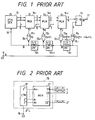
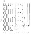
- each gate G1, G3, ---, G2 n -1 to which the clock signal is directly supplied is paired respectively with other each gate G2, G4, ---, G2 n , and both outputs of each pair are supplied to each OR circuit R1, R2, ---, R2 n-1 , respectively. Consequently, each OR circuit R1, R2, ---, R2 n-1 issues an odd-numbered input pattern data in the first half cycle of each clock, while in the latter half cycle even-numbered input pattern data being output. As a result, the input data is multiplexed into 2 n-1 pieces of parallel pattern data. In this case, a delay time ⁇ 1 exists from a rising edge of the clock at terminal 23 to each node of the output pattern data generated in response to said edge.
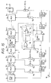
- Q and Q ⁇ outputs of the frequency division circuit 12 n-m are supplied to the phase switching circuit 28 from which either one is selectively output and supplied to the frequency division circuit 12 n-m+1 while at the same time the output is supplied to the 1/2 frequency division circuit 29 via the delay circuit 14 m .
- the output from the frequency division circuit 29 is supplied to the multiplexing circuit 14 m as a multiplexing control clock signal.
- the frequency of the output clock signal from the 1/2 frequency division circuit 29 is the same as the frequency of the output clock signal from the 1/2 frequency division circuit 12 n-m+1 . Therefore, in this embodiment the latter is supplied only to the 1/2 frequency division circuit 12 n-m+2 (not illustrated) in the next stage.
- the Q output of the toggle type flipflop 35 is subjected to retiming by a clock signal B in the D type flipflop 41.
- the Q output and Q ⁇ output are supplied to the gates 36 and 37 of Fig. 6 or the Q ⁇ output is supplied to the exclusive OR circuit 39 of Fig. 12, thereby stabilizing the operation.
- the intermediate retiming circuit 27 shown in Fig. 6 may also be inserted at several locations in the multi-stage connections of the multiplexing circuits.
Landscapes
- Engineering & Computer Science (AREA)
- Physics & Mathematics (AREA)
- General Engineering & Computer Science (AREA)
- General Physics & Mathematics (AREA)
- Theoretical Computer Science (AREA)
- Computer Networks & Wireless Communication (AREA)
- Synchronisation In Digital Transmission Systems (AREA)
Applications Claiming Priority (2)
| Application Number | Priority Date | Filing Date | Title |
|---|---|---|---|
| JP218454/90 | 1990-08-20 | ||
| JP2218454A JP2966491B2 (ja) | 1990-08-20 | 1990-08-20 | 広帯域パルスパターン発生器 |
Publications (2)
| Publication Number | Publication Date |
|---|---|
| EP0472160A2 true EP0472160A2 (de) | 1992-02-26 |
| EP0472160A3 EP0472160A3 (en) | 1993-01-13 |
Family
ID=16720162
Family Applications (1)
| Application Number | Title | Priority Date | Filing Date |
|---|---|---|---|
| EP19910113931 Withdrawn EP0472160A3 (en) | 1990-08-20 | 1991-08-20 | High-rate pulse pattern generator |
Country Status (3)
| Country | Link |
|---|---|
| US (1) | US5150390A (de) |
| EP (1) | EP0472160A3 (de) |
| JP (1) | JP2966491B2 (de) |
Families Citing this family (7)
| Publication number | Priority date | Publication date | Assignee | Title |
|---|---|---|---|---|
| KR0135488B1 (ko) * | 1994-05-26 | 1998-06-15 | 김광호 | 동기카운터 및 그 캐리전파방법 |
| GB2302191B (en) * | 1995-02-24 | 2000-05-10 | Advantest Corp | Bit error measurement system. |
| US6671341B1 (en) * | 1999-09-17 | 2003-12-30 | Agere Systems, Inc. | Glitch-free phase switching synthesizer |
| US6293540B1 (en) * | 1999-11-29 | 2001-09-25 | Diebold, Incorporated | Currency dispenser service method |
| EP1244214A1 (de) * | 2001-03-23 | 2002-09-25 | STMicroelectronics Limited | Phasengesteuerter digitaler Frequenzteiler |
| JP2003198496A (ja) * | 2001-12-27 | 2003-07-11 | Ando Electric Co Ltd | 時分割多重信号発生回路 |
| US8766681B2 (en) * | 2012-09-07 | 2014-07-01 | Applied Micro Circuits Corporation | Device and method for a multiplexor/demultiplexor reset scheme |
Family Cites Families (6)
| Publication number | Priority date | Publication date | Assignee | Title |
|---|---|---|---|---|
| JPS60143017A (ja) * | 1983-12-29 | 1985-07-29 | Advantest Corp | クロツク同期式論理装置 |
| JPS62276935A (ja) * | 1986-01-07 | 1987-12-01 | Fujitsu Ltd | 多重化装置 |
| US4757264A (en) * | 1987-10-08 | 1988-07-12 | American Telephone And Telegraph Company, At&T Bell Laboratories | Sample clock signal generator circuit |
| US4868430A (en) * | 1988-02-11 | 1989-09-19 | Ncr Corporation | Self-correcting digitally controlled timing circuit |
| US5062126A (en) * | 1990-03-26 | 1991-10-29 | Hughes Aircraft Company | High speed synchronous counter system and process with look-ahead carry generating circuit |
| US5060243A (en) * | 1990-05-29 | 1991-10-22 | Motorola, Inc. | Ripple counter with reverse-propagated zero detection |
-
1990
- 1990-08-20 JP JP2218454A patent/JP2966491B2/ja not_active Expired - Fee Related
-
1991
- 1991-08-20 US US07/748,755 patent/US5150390A/en not_active Expired - Fee Related
- 1991-08-20 EP EP19910113931 patent/EP0472160A3/en not_active Withdrawn
Also Published As
| Publication number | Publication date |
|---|---|
| JPH04100406A (ja) | 1992-04-02 |
| JP2966491B2 (ja) | 1999-10-25 |
| US5150390A (en) | 1992-09-22 |
| EP0472160A3 (en) | 1993-01-13 |
Similar Documents
| Publication | Publication Date | Title |
|---|---|---|
| US4604582A (en) | Digital phase correlator | |
| US5422835A (en) | Digital clock signal multiplier circuit | |
| KR100528379B1 (ko) | 클록신호분배시스템 | |
| EP0656688B1 (de) | Taktsignalgenerator für eine Vielzahl nicht überlappender Taktsignale | |
| KR100295121B1 (ko) | 클럭 복구 회로 | |
| US4445215A (en) | Programmable frequency ratio synchronous parallel-to-serial data converter | |
| JPH0630490B2 (ja) | ディジタルpll回路 | |
| EP0711036B1 (de) | Einstellbare Verzögerungsschaltung | |
| US7071750B2 (en) | Method for multiple-phase splitting by phase interpolation and circuit the same | |
| EP0600815A2 (de) | Programmierbarer Pulsgenerator mit hoher Auflösung | |
| US6441657B1 (en) | Combinational delay circuit for a digital frequency multiplier | |
| US20090051347A1 (en) | High frequency delay circuit and test apparatus | |
| US6667639B2 (en) | Frequency multiplying system having a plurality of output frequencies | |
| US5150390A (en) | High-rate pulse pattern generator | |
| US4827490A (en) | Method of synchronizing two binary trains | |
| KR100525096B1 (ko) | Dll 회로 | |
| EP1385306A1 (de) | Verfahren und Einrichtung für die parallele Synchronisation von mehreren seriellen Datenströmen | |
| US5726651A (en) | Device for serializing high flow of binary data | |
| US5163069A (en) | Pattern synchronizing circuit and method | |
| US4698826A (en) | Clock repeater for triplicated clock distributor | |
| US6791384B2 (en) | Delay adjustment circuit for delay locked loop | |
| EP1385308A1 (de) | Verfahren und Einrichtung für die parallele Synchronisation von mehreren seriellen Datenströmen | |
| KR102287515B1 (ko) | 주파수 분주 회로 | |
| EP1385294A1 (de) | Verfahren und Einrichtung zur Phasenjustierung zweier Taktsignale | |
| US20110181365A1 (en) | Synchronization of a Data Output Signal to An Input Clock |
Legal Events
| Date | Code | Title | Description |
|---|---|---|---|
| PUAI | Public reference made under article 153(3) epc to a published international application that has entered the european phase |
Free format text: ORIGINAL CODE: 0009012 |
|
| 17P | Request for examination filed |
Effective date: 19910820 |
|
| AK | Designated contracting states |
Kind code of ref document: A2 Designated state(s): DE FR GB |
|
| PUAL | Search report despatched |
Free format text: ORIGINAL CODE: 0009013 |
|
| AK | Designated contracting states |
Kind code of ref document: A3 Designated state(s): DE FR GB |
|
| STAA | Information on the status of an ep patent application or granted ep patent |
Free format text: STATUS: THE APPLICATION HAS BEEN WITHDRAWN |
|
| 18W | Application withdrawn |
Withdrawal date: 19940525 |