EP0467579B1 - Method of producing optical waveguides by an ion exchange technique on a glass substrate - Google Patents
Method of producing optical waveguides by an ion exchange technique on a glass substrate Download PDFInfo
- Publication number
- EP0467579B1 EP0467579B1 EP91306242A EP91306242A EP0467579B1 EP 0467579 B1 EP0467579 B1 EP 0467579B1 EP 91306242 A EP91306242 A EP 91306242A EP 91306242 A EP91306242 A EP 91306242A EP 0467579 B1 EP0467579 B1 EP 0467579B1
- Authority
- EP
- European Patent Office
- Prior art keywords
- ion exchange
- mask
- zone
- glass substrate
- ions
- Prior art date
- Legal status (The legal status is an assumption and is not a legal conclusion. Google has not performed a legal analysis and makes no representation as to the accuracy of the status listed.)
- Expired - Lifetime
Links
- 238000005342 ion exchange Methods 0.000 title claims description 48
- 238000000034 method Methods 0.000 title claims description 40
- 239000000758 substrate Substances 0.000 title claims description 40
- 239000011521 glass Substances 0.000 title claims description 37
- 230000003287 optical effect Effects 0.000 title claims description 13
- 150000002500 ions Chemical class 0.000 claims description 22
- 238000009792 diffusion process Methods 0.000 claims description 9
- BQCADISMDOOEFD-UHFFFAOYSA-N Silver Chemical compound [Ag] BQCADISMDOOEFD-UHFFFAOYSA-N 0.000 claims description 6
- 229910052709 silver Inorganic materials 0.000 claims description 6
- 239000004332 silver Substances 0.000 claims description 6
- VWDWKYIASSYTQR-UHFFFAOYSA-N sodium nitrate Chemical compound [Na+].[O-][N+]([O-])=O VWDWKYIASSYTQR-UHFFFAOYSA-N 0.000 claims description 6
- 150000003839 salts Chemical class 0.000 claims description 3
- 235000010344 sodium nitrate Nutrition 0.000 claims description 3
- 239000010936 titanium Substances 0.000 claims description 3
- RTAQQCXQSZGOHL-UHFFFAOYSA-N Titanium Chemical compound [Ti] RTAQQCXQSZGOHL-UHFFFAOYSA-N 0.000 claims description 2
- 238000004544 sputter deposition Methods 0.000 claims description 2
- 229910052719 titanium Inorganic materials 0.000 claims description 2
- 239000010408 film Substances 0.000 description 13
- 238000004519 manufacturing process Methods 0.000 description 5
- -1 Tl+ ions Chemical class 0.000 description 4
- 229910052751 metal Inorganic materials 0.000 description 4
- 239000002184 metal Substances 0.000 description 4
- 229910001415 sodium ion Inorganic materials 0.000 description 4
- 239000010410 layer Substances 0.000 description 3
- FOIXSVOLVBLSDH-UHFFFAOYSA-N Silver ion Chemical compound [Ag+] FOIXSVOLVBLSDH-UHFFFAOYSA-N 0.000 description 2
- 230000015572 biosynthetic process Effects 0.000 description 2
- 239000000155 melt Substances 0.000 description 2
- 239000013307 optical fiber Substances 0.000 description 2
- 230000008878 coupling Effects 0.000 description 1
- 238000010168 coupling process Methods 0.000 description 1
- 238000005859 coupling reaction Methods 0.000 description 1
- 238000005516 engineering process Methods 0.000 description 1
- 239000000203 mixture Substances 0.000 description 1
- 239000005304 optical glass Substances 0.000 description 1
- 230000035945 sensitivity Effects 0.000 description 1
- 239000007790 solid phase Substances 0.000 description 1
- 239000002344 surface layer Substances 0.000 description 1
- 238000007669 thermal treatment Methods 0.000 description 1
- 239000010409 thin film Substances 0.000 description 1
Images
Classifications
-
- G—PHYSICS
- G02—OPTICS
- G02B—OPTICAL ELEMENTS, SYSTEMS OR APPARATUS
- G02B6/00—Light guides; Structural details of arrangements comprising light guides and other optical elements, e.g. couplings
- G02B6/10—Light guides; Structural details of arrangements comprising light guides and other optical elements, e.g. couplings of the optical waveguide type
- G02B6/12—Light guides; Structural details of arrangements comprising light guides and other optical elements, e.g. couplings of the optical waveguide type of the integrated circuit kind
- G02B6/13—Integrated optical circuits characterised by the manufacturing method
- G02B6/134—Integrated optical circuits characterised by the manufacturing method by substitution by dopant atoms
- G02B6/1345—Integrated optical circuits characterised by the manufacturing method by substitution by dopant atoms using ion exchange
Definitions
- the invention relates to a method of producing optical waveguides by an ion exchange technique on a glass substrate.
- waveguides are formed by the exchange of the original ions in the glass (typically sodium ions Na+) to ions increasing the refractive index (such as K+, Ag+, Cs+, Rb+, Li+ or Tl+ ions) through a narrow opening in the ion exchange mask, and by using salt melts or a silver film as an ion source.
- thermal treatment or ion exchange in an NaNO3 melt modifies the refractive index profile of the waveguide to obtain better coupling to optical fiber.
- narrow ( ⁇ 2 - 4 ⁇ m) mask openings must be used in the first step.
- the number of exchanged ions is very sensitive to the mask opening width, wherefore there is a marked need of a new production method which allows a wider range of variation for the mask opening width.
- the following article is referred to:
- the object of the invention is to provide a method which reduces the sensitivity of the optical waveguide production process to variation in the width of mask lines or mask openings.
- a method of producing an optical waveguide including a light channel comprising: providing a glass substrate having a first refractive index, diffusing first ions into a surface of said substrate to produce a zone at said surface having a second refractive index greater than said first refractive index, forming an ion diffusion mask on said substrate surface overlying said zone, said mask having a shape narrower than the planar zone, said shape corresponding to a desired light channel in said substrate, and forming the desired light channel by an ion-exchange technique characterised in that said zone is a planar zone and in that said light channel is formed by diffusing said first ions out of the glass substrate, from said surface from portions of said zone not covered by said mask by an ion exchange technique and removing said mask.
- a special feature of the method of the invention is that the light channel is not formed until during the second step of the two-step ion exchange process.
- the diffusion taking place during the formation of the light channel makes the light channel narrower instead of widening it as in prior art ion exchange techniques.
- the tolerances allowed for the width of the mask openings and lines in the thin-film mask technique can be considerably alleviated.
- the width of single-mode diffusion mask openings used in conventional ion exchange technique is about 2 to 4 ⁇ m whereas corresponding single-mode channels are achieved with line widths of about 8 to 10 ⁇ m by means of the method of the invention.
- waveguides are formed by diffusing refractive index increasing ions away from a wider waveguide which has been formed previously on the glass substrate by utilizing an ion exchange technique and a positive-type ion exchange mask.
- the method thereby typically comprises the steps of forming a planar optical waveguide on a glass substrate by the ion exchange technique (with a negative-type ion exchange mask), forming a positive-type'-'-ion exchange mask on said planar waveguide, and removing ions which increase the refractive index of the planar waveguide by the ion exchange technique from glass substrate regions having no ion exchange mask.
- the planar waveguide may cover the whole surface of the substrate.
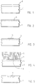
- Figure 1 illustrates the first step of the method of the invention, in which there is formed in a planar glass substrate 1, a planar zone of higher refractive index than the remainder of substrate 1, by introducing refractive-index-increasing ions to the surface of the glass substrate by using the ion exchange technique.
- this first step utilises solid-phase silver ion exchange.
- a thin silver film having a thickness of e.g. about 150 nm is formed by sputtering on the glass substrate 1, such as Corning 0211 glass.
- a metal film (not shown) is formed on the opposite side of the glass substrate 1, and a voltage, e.g.
- the ion exchange mask 4 is of the positive type, that is, it is formed on the substrate 1 at places where the waveguide is to be formed whereas there is no ion exchange mask film at places where no waveguide is to be formed.
- the positive-type ion exchange mask pattern 4 corresponds to a desired optical waveguide pattern.
- the ion exchange mask film can be made e.g. of titanium (Ti).
- the glass substrate 1 provided with the ion exchange mask 4 is subjected to ion exchange in a NaNO3 melt 5.
- Na+ ions thereby propagate from the melt 5 to the surface layer of the glass substrate 1 and to the planar optical waveguide 3.
- refractive index increasing ions such as Ag+ ions, propagate from the surface of the glass substrate 1 and the waveguide 3 into the NaNO3- melt 5.
- the ion exchange takes place only within glass substrate surface regions where there is no ion exchange mask 4. No ion exchange takes place through the ion exchange mask 4, so that a waveguide channel 6 is formed under the ion exchange mask 4.
- the glass substrate 1 is removed from the salt melt 5 and the ion exchange mask 4 is removed, so that the glass substrate now has the desired optical waveguide channel 6, as shown in Figure 5.
- optical waveguides are produced by an ion exchange technique on a glass substrate, wherein the waveguides are formed by diffusing ions increasing the refractive index away from a layer of high refractive index which has been formed previously on the glass substrate and which is wider than the optical waveguides to be produced, the last-noted diffusion step being carried out by using the ion exchange technique and a positive-type ion exchange mask.
- a planar optical waveguide which is not limited in the sideward direction, i.e. is wider than the final optical waveguide to be formed, is formed on the glass substrate by the ion exchange technique.
- a narrow ion exchange mask film is formed on the glass, whereafter the ion exchange is carried out by diffusing ions increasing the refractive index of the planar waveguide out of the glass in regions where there is no ion exchange mask.
- a desired sidewardly limited light channel i.e. a light channel narrower than the planar waveguide, is formed on the glass substrate at places where the ion exchange mask prevents diffusion out of the glass.
Landscapes
- Physics & Mathematics (AREA)
- Engineering & Computer Science (AREA)
- Microelectronics & Electronic Packaging (AREA)
- General Physics & Mathematics (AREA)
- Optics & Photonics (AREA)
- Optical Integrated Circuits (AREA)
- Surface Treatment Of Glass (AREA)
Description
- The invention relates to a method of producing optical waveguides by an ion exchange technique on a glass substrate.
- Interest in the use of ion-exchanged glass waveguides for passive integrated optics has increased considerably recently. Typical examples of such components and devices are single-
mode 1/N power dividers and wavelength selective directional couplers. Since the operation of optical glass waveguides is purely passive, and does not allow adjustment after production, accurate control of production parameters is needed to obtain the desired waveguide reproducibility. This is especially important in the case of directional couplers, in which an accurate control of the propagation constant difference between symmetrical and asymmetrical modes is necessary. To produce optical fiber compatible waveguides by an ion exchange technique, two-step processes are generally used. In these processes, waveguides are formed by the exchange of the original ions in the glass (typically sodium ions Na⁺) to ions increasing the refractive index (such as K⁺, Ag⁺, Cs⁺, Rb⁺, Li⁺ or Tl⁺ ions) through a narrow opening in the ion exchange mask, and by using salt melts or a silver film as an ion source. In the second step, thermal treatment or ion exchange in an NaNO₃ melt modifies the refractive index profile of the waveguide to obtain better coupling to optical fiber. As the diffusion during the second step increases the width of waveguides, narrow (≈ 2 - 4 µm) mask openings must be used in the first step. The number of exchanged ions is very sensitive to the mask opening width, wherefore there is a marked need of a new production method which allows a wider range of variation for the mask opening width. As to the basic principles of the ion exchange technique, the following article is referred to: - Ion-Exchanged Glass Waveguides: A Review, R.V. Ramaswamy, Journal of Lightwave Technology, Vol. 6, No. 6, June 1988, p.984.
- The object of the invention is to provide a method which reduces the sensitivity of the optical waveguide production process to variation in the width of mask lines or mask openings.
- According to the invention, there is provided a method of producing an optical waveguide including a light channel comprising:
providing a glass substrate having a first refractive index,
diffusing first ions into a surface of said substrate to produce a zone at said surface having a second refractive index greater than said first refractive index,
forming an ion diffusion mask on said substrate surface overlying said zone, said mask having a shape narrower than the planar zone, said shape corresponding to a desired light channel in said substrate,
and forming the desired light channel by an ion-exchange technique characterised in that said zone is a planar zone and in that said light channel is formed by diffusing said first ions out of the glass substrate, from said surface from portions of said zone not covered by said mask by an ion exchange technique and removing said mask. - A method corresponding to the preamble of
claim 1 is disclosed in JP-A-58-136 007. - A special feature of the method of the invention is that the light channel is not formed until during the second step of the two-step ion exchange process. As a result, the diffusion taking place during the formation of the light channel makes the light channel narrower instead of widening it as in prior art ion exchange techniques. As a consequence, the tolerances allowed for the width of the mask openings and lines in the thin-film mask technique can be considerably alleviated. For example, the width of single-mode diffusion mask openings used in conventional ion exchange technique is about 2 to 4 µm whereas corresponding single-mode channels are achieved with line widths of about 8 to 10 µm by means of the method of the invention.
- The invention will now be described in greater detail by means of an embodiment with reference to the attached drawing, in which Figures 1 to 5 illustrate the different steps of the method of the invention.
- In the method of the invention for the production of waveguides by an ion exchange technique on a glass substrate, waveguides are formed by diffusing refractive index increasing ions away from a wider waveguide which has been formed previously on the glass substrate by utilizing an ion exchange technique and a positive-type ion exchange mask. The method thereby typically comprises the steps of forming a planar optical waveguide on a glass substrate by the ion exchange technique (with a negative-type ion exchange mask), forming a positive-type'-'-ion exchange mask on said planar waveguide, and removing ions which increase the refractive index of the planar waveguide by the ion exchange technique from glass substrate regions having no ion exchange mask. The planar waveguide may cover the whole surface of the substrate.
- Figure 1 illustrates the first step of the method of the invention, in which there is formed in a
planar glass substrate 1, a planar zone of higher refractive index than the remainder ofsubstrate 1, by introducing refractive-index-increasing ions to the surface of the glass substrate by using the ion exchange technique. In the preferred embodiment of the invention, this first step utilises solid-phase silver ion exchange. For this purpose, a thin silver film having a thickness of e.g. about 150 nm is formed by sputtering on theglass substrate 1, such as Corning 0211 glass. A metal film (not shown) is formed on the opposite side of theglass substrate 1, and a voltage, e.g. 50 V, is connected between thesilver film 2 and the metal film on the opposite side at an elevated temperature (e.g. 350°C). Na⁺ ions thereby start to propagate from theglass substrate 1 to the metal film acting as a cathode, and correspondingly Ag⁺ ions start to propagate from thesilver film 2 to theglass substrate 1, so that aplanar layer 3 having a higher refractive index than that of the surrounding glass is formed on theglass substrate 1. After the formation of the planar layer orzone 3, thesilver film 2 and the metal film on the opposite side of thesubstrate 1 are removed, which results in the situation shown in Figure 2. - Thereafter an ion
exchange mask film 4 is formed on theglass substrate 1 upon theplanar waveguide 3. Theion exchange mask 4 is of the positive type, that is, it is formed on thesubstrate 1 at places where the waveguide is to be formed whereas there is no ion exchange mask film at places where no waveguide is to be formed. Thus the positive-type ionexchange mask pattern 4 corresponds to a desired optical waveguide pattern. The ion exchange mask film can be made e.g. of titanium (Ti). - Thereafter the
glass substrate 1 provided with theion exchange mask 4 is subjected to ion exchange in aNaNO₃ melt 5. Na⁺ ions thereby propagate from themelt 5 to the surface layer of theglass substrate 1 and to the planaroptical waveguide 3. Correspondingly, refractive index increasing ions, such as Ag⁺ ions, propagate from the surface of theglass substrate 1 and thewaveguide 3 into the NaNO₃-melt 5. The ion exchange takes place only within glass substrate surface regions where there is noion exchange mask 4. No ion exchange takes place through theion exchange mask 4, so that awaveguide channel 6 is formed under theion exchange mask 4. After the ion exchange is completed within regions having noion exchange mask 4, theglass substrate 1 is removed from thesalt melt 5 and theion exchange mask 4 is removed, so that the glass substrate now has the desiredoptical waveguide channel 6, as shown in Figure 5. - Thus, in the method described with reference to the drawings, optical waveguides are produced by an ion exchange technique on a glass substrate, wherein the waveguides are formed by diffusing ions increasing the refractive index away from a layer of high refractive index which has been formed previously on the glass substrate and which is wider than the optical waveguides to be produced, the last-noted diffusion step being carried out by using the ion exchange technique and a positive-type ion exchange mask. In the first step of the method, a planar optical waveguide, which is not limited in the sideward direction, i.e. is wider than the final optical waveguide to be formed, is formed on the glass substrate by the ion exchange technique. In the second step, a narrow ion exchange mask film is formed on the glass, whereafter the ion exchange is carried out by diffusing ions increasing the refractive index of the planar waveguide out of the glass in regions where there is no ion exchange mask. A desired sidewardly limited light channel, i.e. a light channel narrower than the planar waveguide, is formed on the glass substrate at places where the ion exchange mask prevents diffusion out of the glass.
- The attached figures and the description related to them are only intended to illustrate the present invention. In its details, the method of the invention may vary within the scope of the attached claims. For instance, the composition of the ion sources, the glass substrate and the ion exchange masks may vary according to the requirements in each particular application.
Claims (5)
- A method of producing an optical waveguide including a light channel comprising:
providing a glass substrate having a first refractive index,
diffusing first ions into a surface of said substrate to produce a zone at said surface having a second refractive index greater than said first refractive index,
forming an ion diffusion mask on said substrate surface overlying said zone, said mask having a shape narrower than the zone, said shape corresponding to a desired light channel in said substrate,
and forming the desired light channel by an ion-exchange technique characterised in that said zone is a planar zone and in that said light channel is formed by diffusing said first ions out of the glass substrate, from said surface from portions of said zone not covered by said mask by an ion exchange technique and removing said mask. - A method according to claim 1 wherein a salt melt or a silver film is used as an ion source for producing said planar zone.
- A method according to claim 1, wherein said planar zone covers substantially the whole surface of the substrate.
- A method according to claim 1 wherein said diffusion of said first ions from said portion of said zone not covered by said mask is performed in an ion exchange process using a NaNO₃ melt placed in contact with said planar zone for providing a source of second ions which are exchanged with said first ions during the second diffusion step.
- A method according to claim 1, wherein the ion mask is made by sputtering from titanium.
Applications Claiming Priority (2)
| Application Number | Priority Date | Filing Date | Title |
|---|---|---|---|
| FI903487A FI86226C (en) | 1990-07-10 | 1990-07-10 | FOERFARANDE FOER FRAMSTAELLNING AV LJUSVAOGSLEDARE MEDELST JONBYTESTEKNIK PAO ETT GLASSUBSTRAT. |
| FI903487 | 1990-07-10 |
Publications (3)
| Publication Number | Publication Date |
|---|---|
| EP0467579A2 EP0467579A2 (en) | 1992-01-22 |
| EP0467579A3 EP0467579A3 (en) | 1992-03-04 |
| EP0467579B1 true EP0467579B1 (en) | 1995-09-27 |
Family
ID=8530784
Family Applications (1)
| Application Number | Title | Priority Date | Filing Date |
|---|---|---|---|
| EP91306242A Expired - Lifetime EP0467579B1 (en) | 1990-07-10 | 1991-07-10 | Method of producing optical waveguides by an ion exchange technique on a glass substrate |
Country Status (5)
| Country | Link |
|---|---|
| US (1) | US5160523A (en) |
| EP (1) | EP0467579B1 (en) |
| JP (1) | JPH04234005A (en) |
| DE (1) | DE69113346T2 (en) |
| FI (1) | FI86226C (en) |
Families Citing this family (93)
| Publication number | Priority date | Publication date | Assignee | Title |
|---|---|---|---|---|
| FR2695384B1 (en) * | 1992-09-04 | 1994-12-09 | Corning Inc | Method for improving the fixing using a fiber optic adhesive to a glass substrate, and integrated optical component treated by this method. |
| DE19609289A1 (en) * | 1996-03-09 | 1997-09-11 | Iot Integrierte Optik Gmbh | Process for manufacturing integrated optical components by ion exchange with a grating mask for layer waveguides |
| CA2217806A1 (en) * | 1997-10-07 | 1999-04-07 | Mark Farries | Grating and method of providing a grating in an ion diffused waveguide |
| US6947651B2 (en) * | 2001-05-10 | 2005-09-20 | Georgia Tech Research Corporation | Optical waveguides formed from nano air-gap inter-layer dielectric materials and methods of fabrication thereof |
| KR100415625B1 (en) * | 2001-08-06 | 2004-01-24 | 한국전자통신연구원 | Method for manufacturing a planar type waveguide using an ion exchange method |
| US8312743B2 (en) * | 2005-05-18 | 2012-11-20 | City University Of Hong Kong | Method for fabricating buried ion-exchanged waveguides using field-assisted annealing |
| GB0718706D0 (en) | 2007-09-25 | 2007-11-07 | Creative Physics Ltd | Method and apparatus for reducing laser speckle |
| US8673163B2 (en) | 2008-06-27 | 2014-03-18 | Apple Inc. | Method for fabricating thin sheets of glass |
| US7810355B2 (en) | 2008-06-30 | 2010-10-12 | Apple Inc. | Full perimeter chemical strengthening of substrates |
| JP5616907B2 (en) | 2009-03-02 | 2014-10-29 | アップル インコーポレイテッド | Technology to strengthen the glass cover of portable electronic devices |
| US9335604B2 (en) | 2013-12-11 | 2016-05-10 | Milan Momcilo Popovich | Holographic waveguide display |
| US11726332B2 (en) | 2009-04-27 | 2023-08-15 | Digilens Inc. | Diffractive projection apparatus |
| US11300795B1 (en) | 2009-09-30 | 2022-04-12 | Digilens Inc. | Systems for and methods of using fold gratings coordinated with output couplers for dual axis expansion |
| US8233204B1 (en) | 2009-09-30 | 2012-07-31 | Rockwell Collins, Inc. | Optical displays |
| US11320571B2 (en) | 2012-11-16 | 2022-05-03 | Rockwell Collins, Inc. | Transparent waveguide display providing upper and lower fields of view with uniform light extraction |
| US10795160B1 (en) | 2014-09-25 | 2020-10-06 | Rockwell Collins, Inc. | Systems for and methods of using fold gratings for dual axis expansion |
| US9778685B2 (en) | 2011-05-04 | 2017-10-03 | Apple Inc. | Housing for portable electronic device with reduced border region |
| US8659826B1 (en) | 2010-02-04 | 2014-02-25 | Rockwell Collins, Inc. | Worn display system and method without requiring real time tracking for boresight precision |
| US9213451B2 (en) | 2010-06-04 | 2015-12-15 | Apple Inc. | Thin glass for touch panel sensors and methods therefor |
| US10189743B2 (en) | 2010-08-18 | 2019-01-29 | Apple Inc. | Enhanced strengthening of glass |
| US8873028B2 (en) | 2010-08-26 | 2014-10-28 | Apple Inc. | Non-destructive stress profile determination in chemically tempered glass |
| US8824140B2 (en) | 2010-09-17 | 2014-09-02 | Apple Inc. | Glass enclosure |
| CN103476727B (en) * | 2011-03-16 | 2016-12-28 | 苹果公司 | Controlled Chemical Strengthening of Thin Glass |
| US9725359B2 (en) | 2011-03-16 | 2017-08-08 | Apple Inc. | Electronic device having selectively strengthened glass |
| US10781135B2 (en) * | 2011-03-16 | 2020-09-22 | Apple Inc. | Strengthening variable thickness glass |
| US9274349B2 (en) | 2011-04-07 | 2016-03-01 | Digilens Inc. | Laser despeckler based on angular diversity |
| US9128666B2 (en) | 2011-05-04 | 2015-09-08 | Apple Inc. | Housing for portable electronic device with reduced border region |
| WO2016020630A2 (en) | 2014-08-08 | 2016-02-11 | Milan Momcilo Popovich | Waveguide laser illuminator incorporating a despeckler |
| WO2013027004A1 (en) | 2011-08-24 | 2013-02-28 | Milan Momcilo Popovich | Wearable data display |
| US10670876B2 (en) | 2011-08-24 | 2020-06-02 | Digilens Inc. | Waveguide laser illuminator incorporating a despeckler |
| US9944554B2 (en) | 2011-09-15 | 2018-04-17 | Apple Inc. | Perforated mother sheet for partial edge chemical strengthening and method therefor |
| US9516149B2 (en) | 2011-09-29 | 2016-12-06 | Apple Inc. | Multi-layer transparent structures for electronic device housings |
| US9715067B1 (en) | 2011-09-30 | 2017-07-25 | Rockwell Collins, Inc. | Ultra-compact HUD utilizing waveguide pupil expander with surface relief gratings in high refractive index materials |
| US9507150B1 (en) | 2011-09-30 | 2016-11-29 | Rockwell Collins, Inc. | Head up display (HUD) using a bent waveguide assembly |
| US8634139B1 (en) | 2011-09-30 | 2014-01-21 | Rockwell Collins, Inc. | System for and method of catadioptric collimation in a compact head up display (HUD) |
| US9366864B1 (en) | 2011-09-30 | 2016-06-14 | Rockwell Collins, Inc. | System for and method of displaying information without need for a combiner alignment detector |
| US10144669B2 (en) | 2011-11-21 | 2018-12-04 | Apple Inc. | Self-optimizing chemical strengthening bath for glass |
| US20150010265A1 (en) | 2012-01-06 | 2015-01-08 | Milan, Momcilo POPOVICH | Contact image sensor using switchable bragg gratings |
| US8684613B2 (en) | 2012-01-10 | 2014-04-01 | Apple Inc. | Integrated camera window |
| US10133156B2 (en) | 2012-01-10 | 2018-11-20 | Apple Inc. | Fused opaque and clear glass for camera or display window |
| US8773848B2 (en) | 2012-01-25 | 2014-07-08 | Apple Inc. | Fused glass device housings |
| US9523852B1 (en) | 2012-03-28 | 2016-12-20 | Rockwell Collins, Inc. | Micro collimator system and method for a head up display (HUD) |
| CN106125308B (en) | 2012-04-25 | 2019-10-25 | 罗克韦尔柯林斯公司 | Apparatus and method for displaying images |
| US9946302B2 (en) | 2012-09-19 | 2018-04-17 | Apple Inc. | Exposed glass article with inner recessed area for portable electronic device housing |
| US9933684B2 (en) | 2012-11-16 | 2018-04-03 | Rockwell Collins, Inc. | Transparent waveguide display providing upper and lower fields of view having a specific light output aperture configuration |
| US9674413B1 (en) | 2013-04-17 | 2017-06-06 | Rockwell Collins, Inc. | Vision system and method having improved performance and solar mitigation |
| US9459661B2 (en) | 2013-06-19 | 2016-10-04 | Apple Inc. | Camouflaged openings in electronic device housings |
| WO2015015138A1 (en) | 2013-07-31 | 2015-02-05 | Milan Momcilo Popovich | Method and apparatus for contact image sensing |
| US9244281B1 (en) | 2013-09-26 | 2016-01-26 | Rockwell Collins, Inc. | Display system and method using a detached combiner |
| US10732407B1 (en) | 2014-01-10 | 2020-08-04 | Rockwell Collins, Inc. | Near eye head up display system and method with fixed combiner |
| US9519089B1 (en) | 2014-01-30 | 2016-12-13 | Rockwell Collins, Inc. | High performance volume phase gratings |
| US9886062B2 (en) | 2014-02-28 | 2018-02-06 | Apple Inc. | Exposed glass article with enhanced stiffness for portable electronic device housing |
| US9244280B1 (en) | 2014-03-25 | 2016-01-26 | Rockwell Collins, Inc. | Near eye display system and method for display enhancement or redundancy |
| WO2016020632A1 (en) | 2014-08-08 | 2016-02-11 | Milan Momcilo Popovich | Method for holographic mastering and replication |
| US10241330B2 (en) | 2014-09-19 | 2019-03-26 | Digilens, Inc. | Method and apparatus for generating input images for holographic waveguide displays |
| US10088675B1 (en) | 2015-05-18 | 2018-10-02 | Rockwell Collins, Inc. | Turning light pipe for a pupil expansion system and method |
| US9715110B1 (en) | 2014-09-25 | 2017-07-25 | Rockwell Collins, Inc. | Automotive head up display (HUD) |
| EP3245444B1 (en) | 2015-01-12 | 2021-09-08 | DigiLens Inc. | Environmentally isolated waveguide display |
| US9632226B2 (en) | 2015-02-12 | 2017-04-25 | Digilens Inc. | Waveguide grating device |
| US11366316B2 (en) | 2015-05-18 | 2022-06-21 | Rockwell Collins, Inc. | Head up display (HUD) using a light pipe |
| US10126552B2 (en) | 2015-05-18 | 2018-11-13 | Rockwell Collins, Inc. | Micro collimator system and method for a head up display (HUD) |
| US10247943B1 (en) | 2015-05-18 | 2019-04-02 | Rockwell Collins, Inc. | Head up display (HUD) using a light pipe |
| US10108010B2 (en) | 2015-06-29 | 2018-10-23 | Rockwell Collins, Inc. | System for and method of integrating head up displays and head down displays |
| US10690916B2 (en) | 2015-10-05 | 2020-06-23 | Digilens Inc. | Apparatus for providing waveguide displays with two-dimensional pupil expansion |
| US10598932B1 (en) | 2016-01-06 | 2020-03-24 | Rockwell Collins, Inc. | Head up display for integrating views of conformally mapped symbols and a fixed image source |
| CN108780224B (en) | 2016-03-24 | 2021-08-03 | 迪吉伦斯公司 | Method and apparatus for providing polarization selective holographic waveguide devices |
| WO2017178781A1 (en) | 2016-04-11 | 2017-10-19 | GRANT, Alastair, John | Holographic waveguide apparatus for structured light projection |
| WO2018013506A1 (en) | 2016-07-15 | 2018-01-18 | Corning Incorporated | Lighting unit with laminate structure |
| KR20190028514A (en) * | 2016-07-15 | 2019-03-18 | 코닝 인코포레이티드 | Laminated optical waveguide article and method for forming the same |
| EP3548939A4 (en) | 2016-12-02 | 2020-11-25 | DigiLens Inc. | WAVE GUIDE DEVICE WITH UNIFORM OUTPUT LIGHTING |
| WO2018129398A1 (en) | 2017-01-05 | 2018-07-12 | Digilens, Inc. | Wearable heads up displays |
| US10295824B2 (en) | 2017-01-26 | 2019-05-21 | Rockwell Collins, Inc. | Head up display with an angled light pipe |
| CN111386495B (en) | 2017-10-16 | 2022-12-09 | 迪吉伦斯公司 | System and method for doubling the image resolution of a pixelated display |
| EP3710876A4 (en) | 2018-01-08 | 2022-02-09 | DigiLens Inc. | SYSTEMS AND METHODS OF FABRICATING WAVEGUIDE CELLS |
| US10914950B2 (en) | 2018-01-08 | 2021-02-09 | Digilens Inc. | Waveguide architectures and related methods of manufacturing |
| KR102745805B1 (en) | 2018-01-08 | 2024-12-20 | 디지렌즈 인코포레이티드. | Method for manufacturing optical waveguide |
| US10732569B2 (en) | 2018-01-08 | 2020-08-04 | Digilens Inc. | Systems and methods for high-throughput recording of holographic gratings in waveguide cells |
| KR102766223B1 (en) | 2018-01-18 | 2025-02-12 | 코닝 인코포레이티드 | Low-loss waveguide formed in high-transmission glass using Ag-Na ion exchange |
| US10690858B2 (en) | 2018-02-28 | 2020-06-23 | Corning Incorporated | Evanescent optical couplers employing polymer-clad fibers and tapered ion-exchanged optical waveguides |
| EP3807707B1 (en) * | 2018-06-15 | 2025-08-06 | Continental Automotive Technologies GmbH | Optical waveguide for a display device |
| US11402801B2 (en) | 2018-07-25 | 2022-08-02 | Digilens Inc. | Systems and methods for fabricating a multilayer optical structure |
| US10585242B1 (en) | 2018-09-28 | 2020-03-10 | Corning Research & Development Corporation | Channel waveguides with bend compensation for low-loss optical transmission |
| US20200225471A1 (en) | 2019-01-14 | 2020-07-16 | Digilens Inc. | Holographic Waveguide Display with Light Control Layer |
| US20200247017A1 (en) | 2019-02-05 | 2020-08-06 | Digilens Inc. | Methods for Compensating for Optical Surface Nonuniformity |
| US20220283377A1 (en) | 2019-02-15 | 2022-09-08 | Digilens Inc. | Wide Angle Waveguide Display |
| CN120405821A (en) | 2019-02-15 | 2025-08-01 | 迪吉伦斯公司 | Method and apparatus for providing holographic waveguide displays using integrated gratings |
| US20200292745A1 (en) | 2019-03-12 | 2020-09-17 | Digilens Inc. | Holographic Waveguide Backlight and Related Methods of Manufacturing |
| US20200386947A1 (en) | 2019-06-07 | 2020-12-10 | Digilens Inc. | Waveguides Incorporating Transmissive and Reflective Gratings and Related Methods of Manufacturing |
| JP2022543571A (en) | 2019-07-29 | 2022-10-13 | ディジレンズ インコーポレイテッド | Method and Apparatus for Multiplying Image Resolution and Field of View for Pixelated Displays |
| KR102775783B1 (en) | 2019-08-29 | 2025-02-28 | 디지렌즈 인코포레이티드. | Vacuum grid and method for manufacturing the same |
| US12399326B2 (en) | 2021-01-07 | 2025-08-26 | Digilens Inc. | Grating structures for color waveguides |
| US12158612B2 (en) | 2021-03-05 | 2024-12-03 | Digilens Inc. | Evacuated periodic structures and methods of manufacturing |
| CN118661138A (en) | 2021-12-29 | 2024-09-17 | 迪吉伦斯公司 | Method and system for holographic recording using an inverted master |
Citations (2)
| Publication number | Priority date | Publication date | Assignee | Title |
|---|---|---|---|---|
| JPS58136007A (en) * | 1982-02-08 | 1983-08-12 | Nippon Sheet Glass Co Ltd | Optical circuit and its manufacture |
| JPS60188906A (en) * | 1984-03-09 | 1985-09-26 | Hitachi Ltd | Plastic optical transmission body and its production |
Family Cites Families (10)
| Publication number | Priority date | Publication date | Assignee | Title |
|---|---|---|---|---|
| US3857689A (en) * | 1971-12-28 | 1974-12-31 | Nippon Selfoc Co Ltd | Ion exchange process for manufacturing integrated optical circuits |
| US4110093A (en) * | 1974-04-22 | 1978-08-29 | Macedo Pedro B | Method for producing an impregnated waveguide |
| JPS58102203A (en) * | 1981-12-14 | 1983-06-17 | Fujitsu Ltd | Formation of waveguide |
| US4376138A (en) * | 1982-01-04 | 1983-03-08 | Bell Telephone Laboratories, Incorporated | Optical waveguides in InGaAsP and InP |
| GB2181861B (en) * | 1985-10-16 | 1989-09-13 | Zeiss Stiftung | Method of making a planar lightwave guide |
| DE3536780A1 (en) * | 1985-10-16 | 1987-04-16 | Schott Glaswerke | METHOD FOR PRODUCING A PLANAR LIGHTWAVE GUIDE |
| IT1195179B (en) * | 1986-09-25 | 1988-10-12 | Cselt Centro Studi Lab Telecom | PROCEDURE FOR THE MANUFACTURE OF OPTICAL GUIDES FOR MEDIUM INFRARED |
| US4842629A (en) * | 1986-12-01 | 1989-06-27 | Siemens Aktiengesellschaft | Method for producing buried regions of raised refractive index in a glass member by ion exchange |
| US4913717A (en) * | 1989-01-23 | 1990-04-03 | Polaroid Corporation | Method for fabricating buried waveguides |
| FI82989C (en) * | 1989-04-13 | 1991-05-10 | Nokia Oy Ab | FRAMEWORK FOR FRAMING REQUIREMENTS AND INSPECTION. |
-
1990
- 1990-07-10 FI FI903487A patent/FI86226C/en not_active IP Right Cessation
-
1991
- 1991-06-10 US US07/713,422 patent/US5160523A/en not_active Expired - Fee Related
- 1991-07-10 EP EP91306242A patent/EP0467579B1/en not_active Expired - Lifetime
- 1991-07-10 JP JP3169705A patent/JPH04234005A/en active Pending
- 1991-07-10 DE DE69113346T patent/DE69113346T2/en not_active Expired - Fee Related
Patent Citations (2)
| Publication number | Priority date | Publication date | Assignee | Title |
|---|---|---|---|---|
| JPS58136007A (en) * | 1982-02-08 | 1983-08-12 | Nippon Sheet Glass Co Ltd | Optical circuit and its manufacture |
| JPS60188906A (en) * | 1984-03-09 | 1985-09-26 | Hitachi Ltd | Plastic optical transmission body and its production |
Also Published As
| Publication number | Publication date |
|---|---|
| EP0467579A3 (en) | 1992-03-04 |
| DE69113346D1 (en) | 1995-11-02 |
| EP0467579A2 (en) | 1992-01-22 |
| FI86226B (en) | 1992-04-15 |
| FI903487L (en) | 1992-01-11 |
| US5160523A (en) | 1992-11-03 |
| FI86226C (en) | 1992-07-27 |
| JPH04234005A (en) | 1992-08-21 |
| DE69113346T2 (en) | 1996-04-04 |
| FI903487A0 (en) | 1990-07-10 |
Similar Documents
| Publication | Publication Date | Title |
|---|---|---|
| US5160523A (en) | Method of producing optical waveguides by an ion exchange technique on a glass substrate | |
| EP0392375B1 (en) | A method of producing optical waveguides | |
| AU604173B2 (en) | Method of making integrated optical component | |
| US6393180B1 (en) | Providing a refractive index change in an ion diffused material | |
| US5151958A (en) | Adaptor device for coupling together optical waveguides produced by k-na ion exchange with optical waveguides produced by ag-na ion exchange | |
| US4136439A (en) | Method for the production of a light conductor structure with interlying electrodes | |
| KR20070091288A (en) | Process and method of waveguide tapering and optimized waveguide structure formation | |
| JP2589367B2 (en) | Optical branching / combining circuit | |
| US6483964B1 (en) | Method of fabricating an optical component | |
| JP2893093B2 (en) | Fabrication method of optical waveguide with fiber guide | |
| JPH0462644B2 (en) | ||
| US5000774A (en) | Method of masked two stage lithium niobate proton exchange | |
| JPH05313032A (en) | Optical waveguide fabrication method | |
| JPH01140124A (en) | Optical device | |
| JPH0197907A (en) | Production of optical waveguide circuit | |
| JP2000158532A (en) | Method for transferring fine pattern and method for manufacturing optical component | |
| GB2191304A (en) | Integrated optical channel waveguide | |
| JPS62119505A (en) | Formation of optical waveguide device | |
| JPH064499B2 (en) | Method for manufacturing gradient index flat lens | |
| JPS63250608A (en) | Production of flush type light guide | |
| JPS6336202A (en) | Production of optical element based on ion exchange | |
| JPH01261243A (en) | Production of optical waveguide | |
| JPH09222523A (en) | Method of manufacturing optical waveguide device | |
| JPS63223713A (en) | Production of light guide | |
| JPH01221706A (en) | Optical waveguide creation method |
Legal Events
| Date | Code | Title | Description |
|---|---|---|---|
| PUAI | Public reference made under article 153(3) epc to a published international application that has entered the european phase |
Free format text: ORIGINAL CODE: 0009012 |
|
| PUAL | Search report despatched |
Free format text: ORIGINAL CODE: 0009013 |
|
| AK | Designated contracting states |
Kind code of ref document: A2 Designated state(s): DE ES FR GB NL SE |
|
| AK | Designated contracting states |
Kind code of ref document: A3 Designated state(s): DE ES FR GB NL SE |
|
| 17P | Request for examination filed |
Effective date: 19920523 |
|
| 17Q | First examination report despatched |
Effective date: 19940112 |
|
| GRAA | (expected) grant |
Free format text: ORIGINAL CODE: 0009210 |
|
| AK | Designated contracting states |
Kind code of ref document: B1 Designated state(s): DE ES FR GB NL SE |
|
| PG25 | Lapsed in a contracting state [announced via postgrant information from national office to epo] |
Ref country code: NL Free format text: LAPSE BECAUSE OF FAILURE TO SUBMIT A TRANSLATION OF THE DESCRIPTION OR TO PAY THE FEE WITHIN THE PRESCRIBED TIME-LIMIT Effective date: 19950927 Ref country code: ES Free format text: THE PATENT HAS BEEN ANNULLED BY A DECISION OF A NATIONAL AUTHORITY Effective date: 19950927 |
|
| REF | Corresponds to: |
Ref document number: 69113346 Country of ref document: DE Date of ref document: 19951102 |
|
| PG25 | Lapsed in a contracting state [announced via postgrant information from national office to epo] |
Ref country code: SE Effective date: 19951227 |
|
| ET | Fr: translation filed | ||
| NLV1 | Nl: lapsed or annulled due to failure to fulfill the requirements of art. 29p and 29m of the patents act | ||
| PGFP | Annual fee paid to national office [announced via postgrant information from national office to epo] |
Ref country code: GB Payment date: 19960628 Year of fee payment: 6 |
|
| PGFP | Annual fee paid to national office [announced via postgrant information from national office to epo] |
Ref country code: FR Payment date: 19960715 Year of fee payment: 6 |
|
| PLBE | No opposition filed within time limit |
Free format text: ORIGINAL CODE: 0009261 |
|
| STAA | Information on the status of an ep patent application or granted ep patent |
Free format text: STATUS: NO OPPOSITION FILED WITHIN TIME LIMIT |
|
| 26N | No opposition filed | ||
| PG25 | Lapsed in a contracting state [announced via postgrant information from national office to epo] |
Ref country code: GB Free format text: LAPSE BECAUSE OF NON-PAYMENT OF DUE FEES Effective date: 19970710 |
|
| GBPC | Gb: european patent ceased through non-payment of renewal fee |
Effective date: 19970710 |
|
| PG25 | Lapsed in a contracting state [announced via postgrant information from national office to epo] |
Ref country code: FR Free format text: LAPSE BECAUSE OF NON-PAYMENT OF DUE FEES Effective date: 19980331 |
|
| REG | Reference to a national code |
Ref country code: FR Ref legal event code: ST |
|
| PGFP | Annual fee paid to national office [announced via postgrant information from national office to epo] |
Ref country code: DE Payment date: 20020717 Year of fee payment: 12 |
|
| PG25 | Lapsed in a contracting state [announced via postgrant information from national office to epo] |
Ref country code: DE Free format text: LAPSE BECAUSE OF NON-PAYMENT OF DUE FEES Effective date: 20040203 |