EP0466329A2 - Apparatus for detecting digital data signals in a analog readback signal - Google Patents
Apparatus for detecting digital data signals in a analog readback signal Download PDFInfo
- Publication number
- EP0466329A2 EP0466329A2 EP91305184A EP91305184A EP0466329A2 EP 0466329 A2 EP0466329 A2 EP 0466329A2 EP 91305184 A EP91305184 A EP 91305184A EP 91305184 A EP91305184 A EP 91305184A EP 0466329 A2 EP0466329 A2 EP 0466329A2
- Authority
- EP
- European Patent Office
- Prior art keywords
- signal
- detecting
- baseline
- readback
- threshold level
- Prior art date
- Legal status (The legal status is an assumption and is not a legal conclusion. Google has not performed a legal analysis and makes no representation as to the accuracy of the status listed.)
- Granted
Links
Images


Classifications
-
- G—PHYSICS
- G11—INFORMATION STORAGE
- G11B—INFORMATION STORAGE BASED ON RELATIVE MOVEMENT BETWEEN RECORD CARRIER AND TRANSDUCER
- G11B20/00—Signal processing not specific to the method of recording or reproducing; Circuits therefor
- G11B20/10—Digital recording or reproducing
- G11B20/10009—Improvement or modification of read or write signals
- G11B20/10046—Improvement or modification of read or write signals filtering or equalising, e.g. setting the tap weights of an FIR filter
- G11B20/10203—Improvement or modification of read or write signals filtering or equalising, e.g. setting the tap weights of an FIR filter baseline correction
Definitions
- the present invention relates to apparatus for detecting digital data signals in an analog readback signal from a data recording device, particularly those signals derived from the use of pulse-width modulation (PWM), to record data in an optical disk recorder.
- PWM pulse-width modulation
- Digital or digitised signal processing has always been sensitive to signal baseline shifts whenever a digital or bipolar readback signal was unbalanced towards one polarity or the other, the shift towards the dominant polarity brings the baseline towards that polarity.
- Digital waveforms also known as binary signals
- NRZI pattern 16 shown in Figure 1 of the accompanying drawings
- the waveform has no baseline shift (as defined below), which means that there are only two levels in that waveform.
- the waveform has a high level denoted HI, a low level denoted LO and transitions between the two levels denoted T.
- Idealised reproduction of a digital waveform requires a noiseless and infinite bandwidth linear analog channel.
- baseline shift can cause an apparent shift in transition positions (the zero axis-crossings shift with baseline shifts).
- One way to accommodate or prevent some of the baseline shifts is to provide balanced codes; i.e., the amount of signal of one polarity is equal to the same amount of signal of the opposite polarity, such that the net DC component of the signal is zero. This increases the overhead of the recorded data. Therefore, it is desirable to provide a data signal detection apparatus which rapidly compensates for any DC shift in signal baseline.
- the simplest way to detect analog data readback signal transitions, which are carrying digital information, for example, is to compare the amplitude of the analog signal waveform with a fixed amplitude threshold. In such detection, each time the analog signal amplitude crosses the threshold, a transition is indicated.
- the slope of the analog signal transition i.e., at the zero axis crossing, depends on many factors, including the read-channel bandwidth and its characteristics. Generally, the lower the bandwidth, the lower the slope. The lower the slope, the more difficult it is to obtain a precise location of the zero axis crossing, as is necessary in detecting pulse-width modulated signals.
- the analog signal baseline DC level
- a common readback data signal transition detection method is to differentiate the received analog signal and then in peaks detect the differentiated signal.
- the differentiated signal is often differentiated a second time in order to obtain a zero axis crossing, which is in time-coincidence with each peak in the differentiated signal.
- binary ones are detected.
- a problem with a detection process using differentiation is the increase in noise associated with the differentiating process.
- the differentiating increases the high-frequency response in the read channel and boosts high frequency noise. Theoretically, a reduction in the signal-to-noise ratio is about six decibels. It is desired to avoid this problem and yet decrease sensitivity to baseline shifting by accommodating this detection process to the baseline shifting.
- Differentiation of a readback signal is also used to time the detection; that is, the zero crossing of the differentiated signal is time coincident with the peak of the readbeack signal.
- US -A- 4,475,183 shows such a system. This system is also subject to phase shifting of the transition position in the detection process, which is to be avoided
- US -A- 4,418,406 shows a signal-wave control circuit having a comparator for receiving an input signal and a second input to the comparator for receiving a reference level signal.
- An output terminal carries the output signal having positive and negative portions corresponding to the input signal.
- a detector detects the maximum or minimum transition interval included in the output signal for producing a detected signal.
- a hold circuit holds the detected signal and a control circuit produces the reference level signal whereby the interval of the positive portion of the output signal and the interval of the negative portion of the output signal become equal.
- the circuit then is a system for removing the effects of DC-baseline shifts and analog signals.
- This circuit requires a balanced run length limited code system which, as discussed above, increases the overhead of the data recording system; therefore, a more flexible baseline accommodation system is desired than that shown in US -A- 4,418,406.
- the object of the present invention is to provide an improved apparatus for detecting digital data signals in a readback signal from a data recording system.
- the present invention relates to apparatus for detecting a digital data signal in the readback signal from a data recording system comprising means for receiving a readback signal containing digital data signals, means for detecting transitions of the readback signal relative to the DC baseline of the readback signal, and means for utilising the transitions to generate the digital data signals.
- the apparatus is characterised in it comprises threshold level generating means dependant on selected parameters of the readback signal for generating a varying threshold level which defines the DC baseline.
- the threshold level generating means holds the value of the threshold until the next sample time. Sampling of the input readback signal is preferred to be achieved by detecting the peaks of the input analog signal or inflection points of the transition.
- positive and negative peak detectors define the peak envelope of the readback analog signal. Peak values are averaged to find the detection threshold level. The threshold level is then used as a reference for detecting baseline crossings at defined sample times.
- the threshold level is averaged between successive transition position areas using the above-mentioned peak value averaging.
- the data signal to be detected is delayed by one detection period. During this one period delay, the DC-baseline tracking occurs.
- the tracking threshold for the signal which was delayed provides accurate amplitude detection of the data in the received and delayed signals.
- portion 10 of an optical data recording disk shows a track having a track centreline 15 with recorded optically-sensible spots 11, 12, 13 and 14.
- the spots 11-14 can be either magneto-optically sensed on a magneto-optic medium, intensity-modulation sensed, such as in an ablative medium, or phase-modulation sensed, such as in a phase-changed medium, for example.
- the recorded spots 11-14 are on a planar surface of portion 10; i.e., no grooves are shown in this particular embodiment, it being understood that either a planar or a grooved optical medium may be employed. Further, the principles described herein may also be used with magnetic recording of some types.
- a recording signal 16 is used to record the spots 11-14 representing the data 17 to be recorded, wherein the binary one is represented by a transition in a transition position, while a binary zero is represented by the absence of a transition in a transition position, along track 15. It is to be understood that the data recorded in marks 11-14 is represented by the durations of the pulses in the recording signal 16; i.e., the space between successive transitions to provide a pulse-width modulated signal.
- the principle of the invention described herein can also be applied to pulse-position modulation, wherein each of the positive peak positions represents a unique portion of the data 17.
- the sensing of the recorded data on portion 10 results in a read or readback signal 18. Because of the imbalance in the recorded waveform and other factors, in the two successive lone one-hatf wavelengths representing the spots 11 and 12, the read signal DC baseline 19 is shifted towards one polarity of the read signal, represented by an upward shift in Figure 1. According to the principle of the present invention, the shifting of the DC baseline 19 is accommodated at each of the transition positions representing a binary one in data 17.
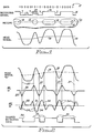
- Figure 2 illustrates a known technique for amplitude-detecting digital data signals in a read or readback signal 18, even with a shifted DC base-line 19. It is to be understood that noise is introduced into the readback channel and the possibility of missing data or of getting erroneous data is relatively high in recording systens which are designed for low density recording. Noise caused by high frequency boost can introduce errors in the data detection process. This shifting is often referred to as jitter.
- the brackets 33 indicate the ranges where unintended transition position changes caused by noise are likely to occur, as represented by hash marks 34 on signal 30.
- the read signal, R is differentiated (dR/dt) to produce a differentiated signal 25 having a constant baseline 26.
- the differentiated signal 25 is again differentiated to obtain signal 30 (dR′/dt) having a baseline 31.
- the zero axis crossings of signal 30 are used to time the detection of the peaks in signal 25 for producing a shape-detected data output signal 32.
- the false zero crossings of signal 30 have to be eliminated, such as by sensing the low-amplitude portion of signal 25.
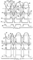
- FIG 3 shows a set of signal waveforms illustrating a digital data signal detection process in accordance with the invention by deriving a detection-tracking amplitude threshold from amplitude samples, such as peak amplitudes, of a readback signal 18.
- the detection process produces a positive signal envelope 40 and a negative signal envelope 41, each envelope is related respectively to the positive and negative peak amplitude values of readback signal 18.
- a detection threshold 42 tracks the imbalance shifting of DC baseline 19 (see Figure 1) by averaging the values of envelope signals 40 and 41, which shift with the DC baseline.
- Readback signal 18 is differentiated to produce differentiated signal 25.
- the zero axis or DC baseline crossings of readback signal 18 are coincident with the peak amplitudes of the differentiated signal 25.
- output pulses 43 and 44 are generated.
- These pulses gate current sources 67 and 83 (see Figure 5) for discharging the storage capacitors 69 and 84 (see Figure 5), respectively.
- These capacitors store the positive and negative read back signal peak values received from detectors 65 and 80, respectively.
- Each capacitor discharge occurs immediately before the next ensuing peak is to be detected. This discharge enables the tracking of lower peak values to occur (more faithfully indicate amptitudes of small amplitude signal peaks); otherwise the storage capacitors 69 and 84 could continue to store a prior higher amplitude peak value.
- the NRZI signal 32 is generated by detecting signal 18 crossing threshold 42.
- the value of the detection-threshold 42 is held between successive zero axis (DC baseline) crossings of read signal 18. At each zero axis crossing of readback signal 18, the value of the DC baseline is measured and the detection threshold 42 adjusted. This amplitude derived threshold 42, therefore, rapidly tracks readback signal 18 baseline shifting since there is a full adjustment at each of the zero axis (DC baseline) crossings of readback signal 18. This adjustment occurs twice for each full cycle of readback signal 18. For example, in Figure 3 the first threshold adjustment (a downward shift) occurs at 42A after the comparison of the peak amplitudes of the readback signal at 40A and 41A. The second adjustment, at 42B, shows an upward shift as viewed in Figure 3, of the detection threshold 42.
- This adjustment is caused by measuring the amplitude difference between peaks 40B and 41B.
- the adjustment at 42A-1 which is minor, is achieved by positive peak detector 65 (see Figure 5) detecting positive peak 40B. This adjustment procedure is repeated throughout the signal processing of readback signal 18. Negative peaks 41A, 41B and 41C are tracked by the negative peak detector 80.
- the averaging circuit (illustrated in Figure 5) consists of positive envelope buffer 68, resistor 72, negative envelope buffer 81, resistor 85 and averaging capacitor 73.
- the DC baseline transition immediately following the baseline measurement is used.
- the DC baseline transition occurring intermediate to adjacent peak amplitudes which have been used to generate the corrected detection threshold 42 is used. It should be noted that the detection of the data and the adjustment of the detection threshold 42 are highly dynamic, such that the detection threshold 42, or adjusted DC baseline, quickly follows the shifts and amplitude values of the readback signal 18.
- Figure 4 shows a set of signal waveforms usable to described the operation of the system illustrated in Figure 6, wherein the detection threshold 50 follows the shifting DC baseline based upon transition sampling.
- This system is just as dynamic as that described for Figure 3.
- readback signal 18 is analysed to produce a tracking or detection threshold 50, which shifts with DC baseline shifting, and is differentiated to produce a signal 25.
- a pair of amplitude thresholds 52 and 53 provide for peak detection of differentiated signal 25 to identify the zero axis or DC baseline crossings of readback signal 18. These values are adjusted at each zero axis crossing of readback signal 18.
- Numerals 54 and 55 represent samples of falling and rising transitions in signal 18, respectively, which are sampled and averaged to derive the detection threshold 50.
- Signal 57 is a unipolar set of signals corresponding to the sampling periods of the positive and negative peaks of differentiated signal 25.
- the NRZI readback data signal 32 is generated by detecting signal 18 crossing the threshold 50.
- Figures 6 and 7 illustrate a detection circuit which uses the Figure 4 technique of data detection which has dynamic baseline shift accommodation.
- an optical disk 60 of which portion 10 is a part, is sensed in the usual manner using a laser (not shown) with a focusable and movable lens 61 and optics 62.
- the operation of focusing and positioning the lens 61 with respect to optical disk 60 is well known and is not described for that reason.
- Optics 62 can be those optics used for magneto-optic signal detection, phase-change signal detection, and the like.
- a detector 63 suitable for all the recording systems senses the recorded data and supplies readback signal 18 to read amplifier 64 which supplies an amplified version to the illustrated detection circuits.
- the positive envelope signal 40 is generated by the circuits including the positive peak detector 65, which supplies its positive-peak detected signal to operational amplifier 68.
- Capacitor 69 holds the detected peak value until the next DC baseline transition is detected.
- differentiator 66 generates signal 25 from readback signal 18, and supplies it to gated current source 67.
- gated current source 67 responds to discharge capacitor 69 rapidly.
- the readback signal 18 positive peak detector 65 recharges capacitor 69 rapidly to the new peak value, such as at 40B of Figure 3. That sensed value is then held until the next positive DC baseline crossing occurs.
- Operational amplifier 68 supplies the sampled and held values stored in capacitor 69 to a resistive averaging circuit, including resistors 72 and 85, and smoothing capacitor 73.
- the value held by smoothing capacitor 73 is the average value representing the detection threshold 42.
- the negative envelope signal 41 is generated by the circuits including readback signal 18 negative peak detector 80, which supplies its value to operational amplifier 81 and storage capacitor 84.
- Capacitor 84 holds the value of the negative peak to the input of operational amplifier 81 in the same manner as described for the positive peaks, but until the next negative transition of readback signal 18 is detected. That is, the value is held until signal 25 has a negative peak amplitude lower than the amplitude threshold 46.
- differentiator 82 differentiates signal 18 and supplies the differentiated signal to gated current source 83.
- Gated current source 83 responds to the signal 25 exceeding the negative threshold 46 to discharge the capacitor 84 rapidly.
- readback signal 18 negative peak detector 80 quickly recharges capacitor 84 for re-establishing the negative envelope value 41 at the just-detected negative peak value of readback signal 18.
- Operational amplifier 81 supplies the signal 41 through resistor 85 to capacitor 73.
- Resistors 72 and 85 have an equal impedance and, therefore, find a median value between the two successively-detected positive and negative peaks in the readback signal 18 for generating threshold 42.
- Compare circuit 74 receives signal 18 over line 75 for comparison with threshold 42.
- the NRZI signal from this comparison is supplied to analog circuit AND 86, which produces a train of pulses on line 88, representing the NRZI data output, which is shown in Figure 3 as signal 32.
- Gaps gate 87 enables AND 86 only when data signals are being sensed, to pass digital signal 32 from comparator 74 to line 88.
- Positive and negative peaks of the signal 25 exceeding the positive and negative thresholds 45 and 46 respectively generate the pulses 43 and 44.
- Pulses 43 and 44 are used to develop a gap gating function through gaps gate 87.
- Gaps gate 87 responds to the signal 25 supplied by differentiator 82 to indicate when a true data signal is being received. Many recordings have gaps or areas of no signal between recorded blocks of signals. Gaps gate 87 detects such gaps and signal blocks in a known manner, such as by envelope detection, by integration, and the like. Gaps gate 87 gates detected signal 32 out of AND gate 86.
- Figure 6 illustrates a circuit for implementing the transition-position detection aspect of the system described above with reference to Figure 4.
- Operational amplifier 64 supplies the amplified readback signal 18 over line 91 to compare circuit 90.
- Readback signal 18 is also supplied to sample and hold circuit S & H 92, which is triggered to sample the signal as described for Figure 4.
- Differentiator 94 creates signal 25, which is compared with the amplitude thresholds 52 and 53 to activate sample gate 95 for both the positive and negative amplitude excursions of signal 25 beyond the thresholds 52 and 53.
- Two successive integrations of the sampled and held amplitudes 54 and 55 are supplied into integration capacitor 93 to supply the signal representing the threshold 50 to compare circuit 90.
- the signal integration in capacitor 93, is a time-amplitude integration to provide an indication of the transitions.
- Capacitor 93 is sufficiently large that detection threshold 50 shifts less dynamically than threshold 42.
- Results of the comparison 90, between the read signal 18 and the threshold 50, are passed to AND 97, as described above for Gaps Gate 87 (see Figure 5). to provide the NRZI pulses 32 AND 97 is gated by the output of Gaps Gate 96.
- Figure 7 shows another circuit which detects zero axis or DC baseline crossings of signal 18.
- Line 75 carries the operational amplifier 64 signal to differentiator 100 which generates signal 25 ( Figure 4).
- signal 25 goes to a pair of peak-amplitude comparison detectors 101 and 102.
- Comparator 101 has a referenre value supplied by potentiometer 103 which generates a voltage threshold 52 (see figure 4). Whenever signal 25 exceeds threshold 52 comparator 101 supplies a signal to OR gate 105 to be sampled, held and averaged in circuit 110. Similarly, for the negative excursions of differentiated signal 25, potentiometer 104 generates voltage threshold 53, which is supplied to the reference input of switching comparator 102.
- Figure 8 illustrates a preferred construction of the sample average and hold circuit 110 illustrated in Figure 7, a known arrangement.
- the readback signal 18 on line 113 is supplied as one input to a switching amplifier 120.
- the peak indicating signal on line 106 supplied by OR circuit 105, turns on charge pump 120 to sample the amplitude of the readback signal 18 and compare it with the current value of the detection threshold 50 on line 112.
- the amplitude difference detected by circuit 120 between the input value and the current reference value adjusts the stored voltage in capacitor 121 during the duration of the peak indicating pulses 57.
- Stored values continue to be supplied to operational amplifier 122, which supplies the tracking detection threshold signal 50 on line 112.
- the Figure 8 illustrated circuits may replace S & H 92 and capacitor 93 of Figure 6.
Abstract
Description
- The present invention relates to apparatus for detecting digital data signals in an analog readback signal from a data recording device, particularly those signals derived from the use of pulse-width modulation (PWM), to record data in an optical disk recorder.
- Digital or digitised signal processing has always been sensitive to signal baseline shifts whenever a digital or bipolar readback signal was unbalanced towards one polarity or the other, the shift towards the dominant polarity brings the baseline towards that polarity.
- Digital waveforms (also known as binary signals), such as the
NRZI pattern 16 shown in Figure 1 of the accompanying drawings, have no baseline shift (as defined below), which means that there are only two levels in that waveform. The waveform has a high level denoted HI, a low level denoted LO and transitions between the two levels denoted T. Idealised reproduction of a digital waveform requires a noiseless and infinite bandwidth linear analog channel. - When a digital waveform passes through an analog channel, such as a magnetic tape write/read channel or an optical disk write/read channel, it experiences distortions. Distortions are caused mainly by limited bandwidth of the channel and the addition of noise. High frequency limits or high frequency roll-offs of the channel cause high frequency (or short wavelength) signals to have less amplitude than low frequency (or long wavelength) signals.
Signal 18 of Figure 1 illustrates high frequency roll-off distortions. AC coupling employed in channels to avoid DC shifts and drifts between different stages of signal processing circuits causes removal of the DC component of the signal and hence baseline shift. A baseline is an imaginary tine connecting average points between two adjacent opposite peaks of an analog waveform. Baseline shift is illustrated by the position of theline 19 in Figure 1. Depending on wavelength and digital sequence, both high frequency roll-off and AC coupling cause analog signals to shift the baseline. - Additional causes of the base line shift of a read backsignal in an optical disk channel are changes in medium reflectivity and bi-refringence of the optical disk substrate. Because of the above reasons, the peaks and transitions in analog waveforms occur at different, often unpredictable, levels and are difficult to detect reliably by conventional fixed threshold detectors.
- In a data signal detecting apparatus, baseline shift can cause an apparent shift in transition positions (the zero axis-crossings shift with baseline shifts). One way to accommodate or prevent some of the baseline shifts is to provide balanced codes; i.e., the amount of signal of one polarity is equal to the same amount of signal of the opposite polarity, such that the net DC component of the signal is zero. This increases the overhead of the recorded data. Therefore, it is desirable to provide a data signal detection apparatus which rapidly compensates for any DC shift in signal baseline.
- The simplest way to detect analog data readback signal transitions, which are carrying digital information, for example, is to compare the amplitude of the analog signal waveform with a fixed amplitude threshold. In such detection, each time the analog signal amplitude crosses the threshold, a transition is indicated. The slope of the analog signal transition; i.e., at the zero axis crossing, depends on many factors, including the read-channel bandwidth and its characteristics. Generally, the lower the bandwidth, the lower the slope. The lower the slope, the more difficult it is to obtain a precise location of the zero axis crossing, as is necessary in detecting pulse-width modulated signals. Also, it is well known that the analog signal baseline (DC level) is constantly moving. The real crossing point between the analog signal and the fixed threshold will shift causing data detection errors. If the analog signal moves entirely above or below the fixed threshold, the transition detection fails. In an optical disk recorder, baseline movements of a readback signal, which is turned into an analog signal, takes place towards either polarity and dynamically change because of the often-used alternating current (AC) coupling, of changes in medium reflectivity and of bi-refringence of the substrate through which a reading or sensing laser beam passes to reach the recording layer of the optical medium.
- Because of the above-described baseline shifting, a common readback data signal transition detection method is to differentiate the received analog signal and then in peaks detect the differentiated signal. The differentiated signal is often differentiated a second time in order to obtain a zero axis crossing, which is in time-coincidence with each peak in the differentiated signal. By detecting the zero axis crossings of the analog readback signal coinciding with the peaks in the differentiated signal, binary ones are detected. A problem with a detection process using differentiation is the increase in noise associated with the differentiating process. The differentiating, of course, increases the high-frequency response in the read channel and boosts high frequency noise. Theoretically, a reduction in the signal-to-noise ratio is about six decibels. It is desired to avoid this problem and yet decrease sensitivity to baseline shifting by accommodating this detection process to the baseline shifting.
- Differentiation of a readback signal is also used to time the detection; that is, the zero crossing of the differentiated signal is time coincident with the peak of the readbeack signal. US -A- 4,475,183 shows such a system. This system is also subject to phase shifting of the transition position in the detection process, which is to be avoided
- US -A- 4,418,406 shows a signal-wave control circuit having a comparator for receiving an input signal and a second input to the comparator for receiving a reference level signal. An output terminal carries the output signal having positive and negative portions corresponding to the input signal. A detector detects the maximum or minimum transition interval included in the output signal for producing a detected signal. A hold circuit holds the detected signal and a control circuit produces the reference level signal whereby the interval of the positive portion of the output signal and the interval of the negative portion of the output signal become equal. The circuit then is a system for removing the effects of DC-baseline shifts and analog signals. This circuit requires a balanced run length limited code system which, as discussed above, increases the overhead of the data recording system; therefore, a more flexible baseline accommodation system is desired than that shown in US -A- 4,418,406.
- The object of the present invention is to provide an improved apparatus for detecting digital data signals in a readback signal from a data recording system.
- The present invention relates to apparatus for detecting a digital data signal in the readback signal from a data recording system comprising means for receiving a readback signal containing digital data signals, means for detecting transitions of the readback signal relative to the DC baseline of the readback signal, and means for utilising the transitions to generate the digital data signals.
- According to the invention the apparatus is characterised in it comprises threshold level generating means dependant on selected parameters of the readback signal for generating a varying threshold level which defines the DC baseline.
- In one aspect of the invention, the threshold level generating means, holds the value of the threshold until the next sample time. Sampling of the input readback signal is preferred to be achieved by detecting the peaks of the input analog signal or inflection points of the transition.
- In some embodiments of the invention, positive and negative peak detectors define the peak envelope of the readback analog signal. Peak values are averaged to find the detection threshold level. The threshold level is then used as a reference for detecting baseline crossings at defined sample times.
- In another embodiment of the invention, the threshold level is averaged between successive transition position areas using the above-mentioned peak value averaging. In a specific form of the invention, the data signal to be detected is delayed by one detection period. During this one period delay, the DC-baseline tracking occurs.
- On the end of the delay, the tracking threshold for the signal which was delayed provides accurate amplitude detection of the data in the received and delayed signals.
- In order that the invention may be more readily understood, embodiments of the invention will now be described with reference to the accompanying drawings, in which:
- Figure 1 is a diagrammatic showing of a portion of an optical disk having pulse-width modulated signals recorded thereon and the resultant readback signal,
- Figure 2 illustrates a known recorded data detection system using differentiated signals,
- Figure 3 is a graph including a plurality of signals used to show the operation of a recorded data detection system according to the invention,
- Figure 4 is a graph including a plurality of signals used to show the operation of a modified detection system in accordance with the invention, and
- Figures 5, 6 and 7 illustrate., in diagrammatic form, three different detection systems implementing the present invention, and
- Figure 8 is a schematic diagram showing a sample, average and hold circuit usable with the detection system illustrated in Figure 7.
- Referring now more particularly to the drawings, like numerals indicate like parts of structural features in the various figures. With reference to Figure 1 portion 10 of an optical data recording disk shows a track having a
track centreline 15 with recorded optically-sensible spots - A
recording signal 16 is used to record the spots 11-14 representing thedata 17 to be recorded, wherein the binary one is represented by a transition in a transition position, while a binary zero is represented by the absence of a transition in a transition position, alongtrack 15. It is to be understood that the data recorded in marks 11-14 is represented by the durations of the pulses in therecording signal 16; i.e., the space between successive transitions to provide a pulse-width modulated signal. The principle of the invention described herein can also be applied to pulse-position modulation, wherein each of the positive peak positions represents a unique portion of thedata 17. - The sensing of the recorded data on portion 10 results in a read or
readback signal 18. Because of the imbalance in the recorded waveform and other factors, in the two successive lone one-hatf wavelengths representing the spots 11 and 12, the readsignal DC baseline 19 is shifted towards one polarity of the read signal, represented by an upward shift in Figure 1. According to the principle of the present invention, the shifting of theDC baseline 19 is accommodated at each of the transition positions representing a binary one indata 17. - Figure 2 illustrates a known technique for amplitude-detecting digital data signals in a read or
readback signal 18, even with a shifted DC base-line 19. It is to be understood that noise is introduced into the readback channel and the possibility of missing data or of getting erroneous data is relatively high in recording systens which are designed for low density recording. Noise caused by high frequency boost can introduce errors in the data detection process. This shifting is often referred to as jitter. Thebrackets 33 indicate the ranges where unintended transition position changes caused by noise are likely to occur, as represented by hash marks 34 on signal 30. The read signal, R, is differentiated (dR/dt) to produce adifferentiated signal 25 having aconstant baseline 26. Thedifferentiated signal 25 is again differentiated to obtain signal 30 (dR′/dt) having abaseline 31. The zero axis crossings of signal 30 are used to time the detection of the peaks insignal 25 for producing a shape-detecteddata output signal 32. The false zero crossings of signal 30 have to be eliminated, such as by sensing the low-amplitude portion ofsignal 25. - Figure 3 shows a set of signal waveforms illustrating a digital data signal detection process in accordance with the invention by deriving a detection-tracking amplitude threshold from amplitude samples, such as peak amplitudes, of a
readback signal 18. Effectively, the detection process produces apositive signal envelope 40 and anegative signal envelope 41, each envelope is related respectively to the positive and negative peak amplitude values ofreadback signal 18. A detection threshold 42 (described below) tracks the imbalance shifting of DC baseline 19 (see Figure 1) by averaging the values of envelope signals 40 and 41, which shift with the DC baseline.Readback signal 18 is differentiated to producedifferentiated signal 25. The zero axis or DC baseline crossings ofreadback signal 18 are coincident with the peak amplitudes of thedifferentiated signal 25. When the peak amplitudes ofdifferentiated signal 25, which are positive-peaks exceeding athreshold 45, and negative-peaks exceeding athreshold 46, occur,output pulses current sources 67 and 83 (see Figure 5) for discharging thestorage capacitors 69 and 84 (see Figure 5), respectively. These capacitors store the positive and negative read back signal peak values received fromdetectors storage capacitors NRZI signal 32 is generated by detectingsignal 18crossing threshold 42. - The value of the detection-
threshold 42 is held between successive zero axis (DC baseline) crossings of readsignal 18. At each zero axis crossing ofreadback signal 18, the value of the DC baseline is measured and thedetection threshold 42 adjusted. This amplitude derivedthreshold 42, therefore, rapidly tracks readback signal 18 baseline shifting since there is a full adjustment at each of the zero axis (DC baseline) crossings ofreadback signal 18. This adjustment occurs twice for each full cycle ofreadback signal 18. For example, in Figure 3 the first threshold adjustment (a downward shift) occurs at 42A after the comparison of the peak amplitudes of the readback signal at 40A and 41A. The second adjustment, at 42B, shows an upward shift as viewed in Figure 3, of thedetection threshold 42. This adjustment is caused by measuring the amplitude difference betweenpeaks positive peak 40B. This adjustment procedure is repeated throughout the signal processing ofreadback signal 18.Negative peaks negative peak detector 80. - Zero axis (DC baseline) crossings and peaks of
readback signal 18 are detected, and thedetection threshold 42 which tracks the DC baseline can be generated by averaging the amplitudes ofpeaks positive envelope buffer 68,resistor 72,negative envelope buffer 81,resistor 85 and averagingcapacitor 73. - In a first embodiment, the DC baseline transition immediately following the baseline measurement is used. In a second embodiment, the DC baseline transition occurring intermediate to adjacent peak amplitudes which have been used to generate the corrected
detection threshold 42 is used. It should be noted that the detection of the data and the adjustment of thedetection threshold 42 are highly dynamic, such that thedetection threshold 42, or adjusted DC baseline, quickly follows the shifts and amplitude values of thereadback signal 18. - Figure 4 shows a set of signal waveforms usable to described the operation of the system illustrated in Figure 6, wherein the
detection threshold 50 follows the shifting DC baseline based upon transition sampling. This system is just as dynamic as that described for Figure 3. In this system,readback signal 18 is analysed to produce a tracking ordetection threshold 50, which shifts with DC baseline shifting, and is differentiated to produce asignal 25. A pair ofamplitude thresholds differentiated signal 25 to identify the zero axis or DC baseline crossings ofreadback signal 18. These values are adjusted at each zero axis crossing ofreadback signal 18.Numerals signal 18, respectively, which are sampled and averaged to derive thedetection threshold 50. After sampling and averaging each transition, it is stored by a sample and hold circuit, later described, which holds the level of the derived tracking ordetection threshold 50.Signal 57 is a unipolar set of signals corresponding to the sampling periods of the positive and negative peaks ofdifferentiated signal 25. The NRZI readback data signal 32 is generated by detectingsignal 18 crossing thethreshold 50. Figures 6 and 7 illustrate a detection circuit which uses the Figure 4 technique of data detection which has dynamic baseline shift accommodation. - Referring next to Figure 5, an
optical disk 60, of which portion 10 is a part, is sensed in the usual manner using a laser (not shown) with a focusable andmovable lens 61 andoptics 62. The operation of focusing and positioning thelens 61 with respect tooptical disk 60 is well known and is not described for that reason.Optics 62 can be those optics used for magneto-optic signal detection, phase-change signal detection, and the like. Adetector 63 suitable for all the recording systems senses the recorded data and supplies readbacksignal 18 to readamplifier 64 which supplies an amplified version to the illustrated detection circuits. - The
positive envelope signal 40 is generated by the circuits including thepositive peak detector 65, which supplies its positive-peak detected signal tooperational amplifier 68.Capacitor 69 holds the detected peak value until the next DC baseline transition is detected. When this next transition is detected,differentiator 66 generatessignal 25 fromreadback signal 18, and supplies it to gatedcurrent source 67. When thesignal 25 exceeds thepositive threshold 45 representing a positive peak in thedifferentiated signal 25, gatedcurrent source 67 responds to dischargecapacitor 69 rapidly. After thestorage capacitor 69 has been partially discharged, thereadback signal 18positive peak detector 65recharges capacitor 69 rapidly to the new peak value, such as at 40B of Figure 3. That sensed value is then held until the next positive DC baseline crossing occurs.Operational amplifier 68 supplies the sampled and held values stored incapacitor 69 to a resistive averaging circuit, includingresistors capacitor 73. The value held by smoothingcapacitor 73 is the average value representing thedetection threshold 42. - The
negative envelope signal 41 is generated by the circuits including readback signal 18negative peak detector 80, which supplies its value tooperational amplifier 81 andstorage capacitor 84.Capacitor 84 holds the value of the negative peak to the input ofoperational amplifier 81 in the same manner as described for the positive peaks, but until the next negative transition ofreadback signal 18 is detected. That is, the value is held untilsignal 25 has a negative peak amplitude lower than theamplitude threshold 46. Again,differentiator 82 differentiatessignal 18 and supplies the differentiated signal to gatedcurrent source 83. Gatedcurrent source 83 responds to thesignal 25 exceeding thenegative threshold 46 to discharge thecapacitor 84 rapidly. After thestorage capacitor 84 is partially discharged,readback signal 18negative peak detector 80 quickly rechargescapacitor 84 for re-establishing thenegative envelope value 41 at the just-detected negative peak value ofreadback signal 18.Operational amplifier 81 supplies thesignal 41 throughresistor 85 tocapacitor 73.Resistors readback signal 18 for generatingthreshold 42. - The data detection is achieved by three elements of Figure 5. Compare
circuit 74 receivessignal 18 overline 75 for comparison withthreshold 42. The NRZI signal from this comparison is supplied to analog circuit AND 86, which produces a train of pulses online 88, representing the NRZI data output, which is shown in Figure 3 assignal 32.Gaps gate 87 enables AND 86 only when data signals are being sensed, to passdigital signal 32 fromcomparator 74 toline 88. Positive and negative peaks of thesignal 25 exceeding the positive andnegative thresholds pulses Pulses gaps gate 87.Gaps gate 87 responds to thesignal 25 supplied bydifferentiator 82 to indicate when a true data signal is being received. Many recordings have gaps or areas of no signal between recorded blocks of signals.Gaps gate 87 detects such gaps and signal blocks in a known manner, such as by envelope detection, by integration, and the like.Gaps gate 87 gates detectedsignal 32 out of ANDgate 86. - Figure 6 illustrates a circuit for implementing the transition-position detection aspect of the system described above with reference to Figure 4.
Operational amplifier 64 supplies the amplifiedreadback signal 18 over line 91 to comparecircuit 90.Readback signal 18 is also supplied to sample and hold circuit S &H 92, which is triggered to sample the signal as described for Figure 4.Differentiator 94 createssignal 25, which is compared with theamplitude thresholds sample gate 95 for both the positive and negative amplitude excursions ofsignal 25 beyond thethresholds amplitudes integration capacitor 93 to supply the signal representing thethreshold 50 to comparecircuit 90. Note that the signal integration, incapacitor 93, is a time-amplitude integration to provide an indication of the transitions.Capacitor 93 is sufficiently large thatdetection threshold 50 shifts less dynamically thanthreshold 42. Results of thecomparison 90, between the readsignal 18 and thethreshold 50, are passed to AND 97, as described above for Gaps Gate 87 (see Figure 5). to provide theNRZI pulses 32 AND 97 is gated by the output ofGaps Gate 96. - Figure 7 shows another circuit which detects zero axis or DC baseline crossings of
signal 18.Line 75 carries theoperational amplifier 64 signal todifferentiator 100 which generates signal 25 (Figure 4).signal 25 goes to a pair of peak-amplitude comparison detectors Comparator 101 has a referenre value supplied bypotentiometer 103 which generates a voltage threshold 52 (see figure 4). Wheneversignal 25 exceedsthreshold 52comparator 101 supplies a signal to ORgate 105 to be sampled, held and averaged incircuit 110. Similarly, for the negative excursions ofdifferentiated signal 25,potentiometer 104 generatesvoltage threshold 53, which is supplied to the reference input of switchingcomparator 102. Wheneversignal 25 exceedsthreshold 53, a signal is supplied to ORcircuit 105 to be passed to sample, average andhold circuit 110. It should be noted that these signals are of the same duration and same amplitude; therefore, these signals are representative of the readback signal transition positions, as opposed to the peak amplitudes used with the Figure 5 illustrated system. - Figure 8 illustrates a preferred construction of the sample average and
hold circuit 110 illustrated in Figure 7, a known arrangement. Thereadback signal 18 on line 113 is supplied as one input to a switchingamplifier 120. The peak indicating signal online 106, supplied by ORcircuit 105, turns oncharge pump 120 to sample the amplitude of thereadback signal 18 and compare it with the current value of thedetection threshold 50 online 112. The amplitude difference detected bycircuit 120 between the input value and the current reference value adjusts the stored voltage in capacitor 121 during the duration of thepeak indicating pulses 57. Stored values continue to be supplied tooperational amplifier 122, which supplies the trackingdetection threshold signal 50 online 112. The Figure 8 illustrated circuits may replace S &H 92 andcapacitor 93 of Figure 6.
Claims (7)
- Apparatus for detecting digital data signals in an analog readback signal from a data recording system comprising
means for receiving a readback signal (18) containing digital data signals,
means for detecting transitions of said readback signal relative to the DC baseline of said readback signal, and
means for utilising said transitions to generate said digital data signals (32),
characterised in that said apparatus comprises threshold level generating means dependant on selected parameters of said readback signal for generating a varying threshold level (42; 50) which defines said DC baseline. - Apparatus as claimed in Claim 1 comprising means (72; 93) for storing and using a generated threshold level until the parameters of said readback signal change resulting r-n the generation of a new threshold level.
- Apparatus as claimed in either of the preceding claims characterised in that said threshold level generating means comprises
first detecting means (65, 80) for detecting positive and negative peaks in said readback signal,
second detecting means (66, 82) for detecting baseline crossings of said readback signal. and
generating means (67, 68, 69, 72, 81, 83, 84, 85, 73) for using the outputs from said first and second detecting means to generate said threshold level. - Apparatus as claimed in Claim 3 characterised in that said generating means comprises
storage means (69, 84) for storing values representing said positive and negative peaks to define said threshold level, and
means (66, 67) for changing said stored values when said baseline crossings are detected. - Apparatus as claimed in Claim 1 or Claim 2 characterised in that said threshold level generating means comprises
third detecting means (94) for detecting baseline crossings of said readback signal, and
means 90, 92, 93) for using the outputs from said third detecting means to generate said threshold level. - An apparatus for detecting digital data signals, including in combination:
means for receiving a data signal carrying digital information to be detected;
means for differentiating the received data signal to supply a differentiated signal;
peak circuit means receiving the differentiated signal and detecting the positive and negative peaks thereof to produce a sampling aperture, which coincides with transitions in received data signal for each detected peak;
sample and hold circuit means connected to the receiving means to receive said received data signal and connected to the peak circuit means for responding to each sampling aperture signal to sample and store the then-current value of the delayed received data signal as a baseline indicating value; and
detection circuit means connected to the sample and hold circuit means to detect the value of the data indicated by the received data signal using said baseline indicating value for a next-occurring transition-indicating zero axis crossing of the received data signal. - In apparatus for detecting transitions in a data signal having detection periods in which data is detectable, including, in combination:
first means for analysing a signal envelope of the data signal in each detection period of the signal and establishing an amplitude detection threshold having a predetermined amplitude relationship to said analysed signal envelope for a next ensuing detection period; and
second means for amplitude comparing said data signal and said amplitude detection threshold in a next-occurring detection period of the data signal.
Applications Claiming Priority (2)
| Application Number | Priority Date | Filing Date | Title |
|---|---|---|---|
| US535697 | 1990-06-11 | ||
| US07/535,697 US5101395A (en) | 1990-06-11 | 1990-06-11 | Data detection employing high-speed baseline tracking compensation |
Publications (3)
| Publication Number | Publication Date |
|---|---|
| EP0466329A2 true EP0466329A2 (en) | 1992-01-15 |
| EP0466329A3 EP0466329A3 (en) | 1993-03-03 |
| EP0466329B1 EP0466329B1 (en) | 1998-01-21 |
Family
ID=24135386
Family Applications (1)
| Application Number | Title | Priority Date | Filing Date |
|---|---|---|---|
| EP91305184A Expired - Lifetime EP0466329B1 (en) | 1990-06-11 | 1991-06-10 | Apparatus for detecting digital data signals in a analog signal |
Country Status (4)
| Country | Link |
|---|---|
| US (1) | US5101395A (en) |
| EP (1) | EP0466329B1 (en) |
| JP (1) | JP2826202B2 (en) |
| DE (1) | DE69128744D1 (en) |
Cited By (7)
| Publication number | Priority date | Publication date | Assignee | Title |
|---|---|---|---|---|
| EP0589749A1 (en) * | 1992-09-25 | 1994-03-30 | Thomson-Csf | Analog-digital encoding circuit with zero-offset compensation |
| EP0692787A2 (en) * | 1994-05-06 | 1996-01-17 | Discovision Associates | Method and apparatus for retrieving data from a storage device |
| EP0767461A2 (en) * | 1995-10-02 | 1997-04-09 | Aiwa Co., Ltd. | A method and apparatus for signal threshold adjustement that compensates for signal asymmetry |
| EP0785548A3 (en) * | 1996-01-16 | 1997-08-20 | Ibm | |
| US5790495A (en) * | 1994-05-06 | 1998-08-04 | Discovision Associates | Data generator assembly for retrieving stored data by comparing threshold signal with preprocessed signal having DC component |
| AU739530B2 (en) * | 1994-05-06 | 2001-10-18 | Discovision Associates | An apparatus for retrieving stored data from an information storage medium |
| EP1148682A2 (en) * | 2000-04-17 | 2001-10-24 | Texas Instruments Incorporated | Adaptive data slicer with two peak detectors and averaging means to obtain the optimal threshold |
Families Citing this family (23)
| Publication number | Priority date | Publication date | Assignee | Title |
|---|---|---|---|---|
| EP0817179B1 (en) * | 1991-05-10 | 2001-07-25 | Discovision Associates | Optical data storage and retrieval system and method |
| US5537379A (en) * | 1991-05-10 | 1996-07-16 | Discovision Associates | Optical data storage and retrieval system and method |
| JPH05101312A (en) * | 1991-10-11 | 1993-04-23 | Sony Corp | Data reproducing device |
| US5497361A (en) * | 1992-03-13 | 1996-03-05 | Hitachi, Ltd. | Information reproducing apparatus with a DC level correcting capability |
| JP2810270B2 (en) * | 1992-03-13 | 1998-10-15 | 株式会社日立製作所 | Signal playback method |
| US5357150A (en) * | 1992-11-06 | 1994-10-18 | International Business Machines Corporation | Defect tolerant envelope follower |
| US5424881A (en) | 1993-02-01 | 1995-06-13 | Cirrus Logic, Inc. | Synchronous read channel |
| US5530601A (en) * | 1993-09-30 | 1996-06-25 | International Business Machines Corporation | Tracking threshold circuit for peak detection |
| JP2638520B2 (en) * | 1994-11-22 | 1997-08-06 | 日本電気株式会社 | Optical information recording medium playback device |
| US6151177A (en) * | 1994-12-09 | 2000-11-21 | Seagate Technology, Inc. | Apparatus for compensating for non-linear characteristics of magnetoresistive heads |
| JP3046515B2 (en) * | 1994-12-16 | 2000-05-29 | シャープ株式会社 | Reproducing circuit of optical information recording / reproducing device |
| US5612845A (en) * | 1994-12-27 | 1997-03-18 | International Business Machines Corporation | Method and apparatus for in-situ detection of data storage system spindle motor performance degradation |
| US5943177A (en) | 1995-05-26 | 1999-08-24 | Maxtor Corporation | MR head read signal preconditioning circuitry for reducing pulse -to-pulse baseline distortion |
| US5877644A (en) * | 1997-01-08 | 1999-03-02 | International Business Machines Corporation | Programmable digital envelope following threshold generation apparatus and method |
| WO2004014066A2 (en) * | 2002-07-31 | 2004-02-12 | Koninklijke Philips Electronics N.V. | Method and devic the for setting the slice level in a binary signal |
| US20070055471A1 (en) * | 2003-05-09 | 2007-03-08 | Koninklijke Philips Electronics N.V. | Copy window setpoint control for domain expansion reading |
| US7626899B2 (en) * | 2003-08-06 | 2009-12-01 | Chin-Yin Tsai | Method for obtaining an optimum focusing point of an optical pickup unit and a servo system of an optical disk drive using this method |
| US20130088363A1 (en) * | 2011-10-06 | 2013-04-11 | Alexander Gonzalez | Telemetry Method and System for Well Logging |
| US8493247B2 (en) * | 2011-12-20 | 2013-07-23 | General Electric Company | Methods and systems for decoding data |
| US10234513B2 (en) | 2012-03-20 | 2019-03-19 | Allegro Microsystems, Llc | Magnetic field sensor integrated circuit with integral ferromagnetic material |
| US9812588B2 (en) | 2012-03-20 | 2017-11-07 | Allegro Microsystems, Llc | Magnetic field sensor integrated circuit with integral ferromagnetic material |
| US20140032117A1 (en) * | 2012-07-26 | 2014-01-30 | Baker Hughes Incorporated | SP Curve Drift Correction |
| JP6883248B2 (en) * | 2018-03-26 | 2021-06-09 | 株式会社Jvcケンウッド | Particle measuring machine, analyzer, and analysis method |
Citations (6)
| Publication number | Priority date | Publication date | Assignee | Title |
|---|---|---|---|---|
| US3838448A (en) * | 1973-02-07 | 1974-09-24 | Control Data Corp | Compensated baseline circuit |
| US4087840A (en) * | 1976-06-16 | 1978-05-02 | Carnegie-Mellon University | Method and apparatus for magnetically recording and reproducing physiological information |
| GB2062421A (en) * | 1979-10-26 | 1981-05-20 | Sony Corp | Data extracting circuits; thresholding |
| DE3203559A1 (en) * | 1982-02-03 | 1983-08-11 | Siemens AG, 1000 Berlin und 8000 München | Method and circuit arrangement for converting analog scanning signals into binary squarewave signals |
| FR2565746A1 (en) * | 1984-06-06 | 1985-12-13 | Sud Sa Systemes | Method and device for processing an analog electrical signal and application to the reading of bar codes |
| GB2172467A (en) * | 1985-03-11 | 1986-09-17 | Mcdonald Richard Albert | Dynamic threshold binary video signal generator |
Family Cites Families (8)
| Publication number | Priority date | Publication date | Assignee | Title |
|---|---|---|---|---|
| US3719934A (en) * | 1967-09-18 | 1973-03-06 | Burroughs Corp | System for processing signals having peaks indicating binary data |
| US4445111A (en) * | 1980-09-15 | 1984-04-24 | John Fluke Mfg. Co., Inc. | Bi-polar electronic signal converters with single polarity accurate reference source |
| JPS5757025A (en) * | 1980-09-24 | 1982-04-06 | Sony Corp | Waveform converting circuit |
| US4323885A (en) * | 1980-09-29 | 1982-04-06 | Bell Telephone Laboratories, Incorporated | Noise and crosstalk reduction in mid-riser biased encoders |
| US4475183A (en) * | 1981-10-26 | 1984-10-02 | Eastman Kodak Company | Optical disk retrieval methods, media and systems employing digital data of high fractional bandwidth |
| US4646281A (en) * | 1984-02-08 | 1987-02-24 | Laser Magnetic Storage International Company | Read channel for an optical recorder |
| JPS6232633U (en) * | 1985-08-13 | 1987-02-26 | ||
| JPS62254514A (en) * | 1986-04-28 | 1987-11-06 | Hitachi Ltd | Slice level automatic setting circuit |
-
1990
- 1990-06-11 US US07/535,697 patent/US5101395A/en not_active Expired - Fee Related
-
1991
- 1991-05-10 JP JP3105642A patent/JP2826202B2/en not_active Expired - Fee Related
- 1991-06-10 EP EP91305184A patent/EP0466329B1/en not_active Expired - Lifetime
- 1991-06-10 DE DE69128744T patent/DE69128744D1/en not_active Expired - Lifetime
Patent Citations (6)
| Publication number | Priority date | Publication date | Assignee | Title |
|---|---|---|---|---|
| US3838448A (en) * | 1973-02-07 | 1974-09-24 | Control Data Corp | Compensated baseline circuit |
| US4087840A (en) * | 1976-06-16 | 1978-05-02 | Carnegie-Mellon University | Method and apparatus for magnetically recording and reproducing physiological information |
| GB2062421A (en) * | 1979-10-26 | 1981-05-20 | Sony Corp | Data extracting circuits; thresholding |
| DE3203559A1 (en) * | 1982-02-03 | 1983-08-11 | Siemens AG, 1000 Berlin und 8000 München | Method and circuit arrangement for converting analog scanning signals into binary squarewave signals |
| FR2565746A1 (en) * | 1984-06-06 | 1985-12-13 | Sud Sa Systemes | Method and device for processing an analog electrical signal and application to the reading of bar codes |
| GB2172467A (en) * | 1985-03-11 | 1986-09-17 | Mcdonald Richard Albert | Dynamic threshold binary video signal generator |
Cited By (32)
| Publication number | Priority date | Publication date | Assignee | Title |
|---|---|---|---|---|
| EP0589749A1 (en) * | 1992-09-25 | 1994-03-30 | Thomson-Csf | Analog-digital encoding circuit with zero-offset compensation |
| FR2696300A1 (en) * | 1992-09-25 | 1994-04-01 | Thomson Csf | Analog-digital coding circuit with automatic compensation for zero offset. |
| US5424738A (en) * | 1992-09-25 | 1995-06-13 | Thomson-Csf | Analog-digital encoding circuit with automatic compensation for the zero offset |
| EP0817186A3 (en) * | 1994-05-06 | 2002-03-13 | Discovision Associates | Method for retrieving data from a storage device |
| EP0817188A3 (en) * | 1994-05-06 | 2002-03-13 | Discovision Associates | Apparatus for retrieving data from a storage device |
| US5894468A (en) * | 1994-05-06 | 1999-04-13 | Discovision Associates | Data recovery with differentiation and partial integration stages to eliminate noises and DC offset level |
| US5659535A (en) * | 1994-05-06 | 1997-08-19 | Discovision Associates | Method for retrieving data from a storage device |
| EP1288943A3 (en) * | 1994-05-06 | 2012-07-18 | Discovision Associates | Retrieving data from a storage device using programmable filter and equalizer |
| US6542451B1 (en) | 1994-05-06 | 2003-04-01 | Discovision Associates | Retrieving data from a storage device using programmable filter and equalizer |
| US5706267A (en) * | 1994-05-06 | 1998-01-06 | Discovision Associates | Method and apparatus for retrieving data from a storage device |
| EP0817188A2 (en) * | 1994-05-06 | 1998-01-07 | Discovision Associates | Apparatus for retrieving data from a storage device |
| EP0817190A2 (en) * | 1994-05-06 | 1998-01-07 | Discovision Associates | Method and apparatus for retrieving data from a storage medium |
| EP0817186A2 (en) * | 1994-05-06 | 1998-01-07 | Discovision Associates | Method for retrieving data from a storage device |
| EP0817187A2 (en) * | 1994-05-06 | 1998-01-07 | Discovision Associates | Apparatus and method for retrieving stored data |
| AU739530B2 (en) * | 1994-05-06 | 2001-10-18 | Discovision Associates | An apparatus for retrieving stored data from an information storage medium |
| EP1288943A2 (en) * | 1994-05-06 | 2003-03-05 | Discovision Associates | Retrieving data from a storage device using programmable filter and equalizer |
| US5790495A (en) * | 1994-05-06 | 1998-08-04 | Discovision Associates | Data generator assembly for retrieving stored data by comparing threshold signal with preprocessed signal having DC component |
| EP0817190A3 (en) * | 1994-05-06 | 2002-03-13 | Discovision Associates | Method and apparatus for retrieving data from a storage medium |
| EP0817187A3 (en) * | 1994-05-06 | 2002-03-13 | Discovision Associates | Apparatus and method for retrieving stored data |
| EP0817189A2 (en) * | 1994-05-06 | 1998-01-07 | Discovision Associates | Method for retrieving data from a storage device |
| EP0692787A3 (en) * | 1994-05-06 | 1996-03-20 | Discovision Ass | Method and apparatus for retrieving data from a storage device |
| EP0692787A2 (en) * | 1994-05-06 | 1996-01-17 | Discovision Associates | Method and apparatus for retrieving data from a storage device |
| AU741101B2 (en) * | 1994-05-06 | 2001-11-22 | Discovision Associates | A method for retrieving data stored on a medium |
| EP0817189A3 (en) * | 1994-05-06 | 2002-03-06 | Discovision Associates | Method for retrieving data from a storage device |
| EP0767461A3 (en) * | 1995-10-02 | 1997-08-20 | Aiwa Co | A method and apparatus for signal threshold adjustement that compensates for signal asymmetry |
| EP0767461A2 (en) * | 1995-10-02 | 1997-04-09 | Aiwa Co., Ltd. | A method and apparatus for signal threshold adjustement that compensates for signal asymmetry |
| US5757751A (en) * | 1996-01-16 | 1998-05-26 | International Business Machines Corporation | Baseline correction circuit for pulse width modulated data readback systems |
| EP0785548A3 (en) * | 1996-01-16 | 1997-08-20 | Ibm | |
| US6181177B1 (en) | 1996-01-16 | 2001-01-30 | International Business Machines Corporation | Baseline correction circuit for PWM data readback systems |
| EP1148682A3 (en) * | 2000-04-17 | 2001-10-31 | Texas Instruments Incorporated | Adaptive data slicer with two peak detectors and averaging means to obtain the optimal threshold |
| EP1148682A2 (en) * | 2000-04-17 | 2001-10-24 | Texas Instruments Incorporated | Adaptive data slicer with two peak detectors and averaging means to obtain the optimal threshold |
| US6735260B1 (en) | 2000-04-17 | 2004-05-11 | Texas Instruments Incorporated | Adaptive data slicer |
Also Published As
| Publication number | Publication date |
|---|---|
| EP0466329B1 (en) | 1998-01-21 |
| JPH0590918A (en) | 1993-04-09 |
| EP0466329A3 (en) | 1993-03-03 |
| DE69128744D1 (en) | 1998-02-26 |
| US5101395A (en) | 1992-03-31 |
| JP2826202B2 (en) | 1998-11-18 |
Similar Documents
| Publication | Publication Date | Title |
|---|---|---|
| EP0466329A2 (en) | Apparatus for detecting digital data signals in a analog readback signal | |
| EP0284279B2 (en) | Pulse detection circuit using amplitude and time qualification | |
| US4346411A (en) | Amplitude sensitive three-level detector for derivative read back channel of magnetic storage device | |
| EP0581455A1 (en) | Digital information reproducing apparatus | |
| CA1275730C (en) | Reading circuit in an optical disk apparatus | |
| US5568465A (en) | Reading from record medium in either an inverted or non-inverted signal-processing mode | |
| JPH01169741A (en) | Track polarity detector | |
| JPH01105362A (en) | Stored information reading circuit | |
| US4785252A (en) | Waveform processing circuit | |
| KR100249224B1 (en) | The method and apparatus for detecting mirror signal | |
| JPS6224444A (en) | Device for detecting track crossing direction | |
| US6434098B2 (en) | Optical disc device | |
| JPH09219027A (en) | Off-track detecting circuit | |
| JP3075353B2 (en) | Information recording / reproducing apparatus and information recording / reproducing method | |
| JP2817688B2 (en) | Optical disk recording power control device | |
| KR100318202B1 (en) | Apparatus Of Generating Mirror Signal In Optical Disc System | |
| JP2664221B2 (en) | Information playback device | |
| JPH1064193A (en) | Binarization circuit | |
| JP2560821B2 (en) | Data storage device test equipment | |
| US20050088924A1 (en) | Optical disk apparatus, signal processing apparatus, and playback control method for optical disk apparatus | |
| KR19990062574A (en) | Data slice circuit and data slice method | |
| JPH02254635A (en) | Pregroup crossing signal detector | |
| JPH0258733A (en) | Optical information reproducing device | |
| JPH0722257B2 (en) | Signal level determination device | |
| JPH06243504A (en) | Device for recording and reproducing optical disk |
Legal Events
| Date | Code | Title | Description |
|---|---|---|---|
| PUAI | Public reference made under article 153(3) epc to a published international application that has entered the european phase |
Free format text: ORIGINAL CODE: 0009012 |
|
| AK | Designated contracting states |
Kind code of ref document: A2 Designated state(s): DE FR GB |
|
| 17P | Request for examination filed |
Effective date: 19911219 |
|
| PUAL | Search report despatched |
Free format text: ORIGINAL CODE: 0009013 |
|
| AK | Designated contracting states |
Kind code of ref document: A3 Designated state(s): DE FR GB |
|
| 17Q | First examination report despatched |
Effective date: 19941017 |
|
| GRAG | Despatch of communication of intention to grant |
Free format text: ORIGINAL CODE: EPIDOS AGRA |
|
| GRAG | Despatch of communication of intention to grant |
Free format text: ORIGINAL CODE: EPIDOS AGRA |
|
| GRAH | Despatch of communication of intention to grant a patent |
Free format text: ORIGINAL CODE: EPIDOS IGRA |
|
| GRAH | Despatch of communication of intention to grant a patent |
Free format text: ORIGINAL CODE: EPIDOS IGRA |
|
| GRAA | (expected) grant |
Free format text: ORIGINAL CODE: 0009210 |
|
| AK | Designated contracting states |
Kind code of ref document: B1 Designated state(s): DE FR GB |
|
| PG25 | Lapsed in a contracting state [announced via postgrant information from national office to epo] |
Ref country code: FR Free format text: LAPSE BECAUSE OF FAILURE TO SUBMIT A TRANSLATION OF THE DESCRIPTION OR TO PAY THE FEE WITHIN THE PRESCRIBED TIME-LIMIT Effective date: 19980121 |
|
| REF | Corresponds to: |
Ref document number: 69128744 Country of ref document: DE Date of ref document: 19980226 |
|
| PG25 | Lapsed in a contracting state [announced via postgrant information from national office to epo] |
Ref country code: DE Free format text: LAPSE BECAUSE OF FAILURE TO SUBMIT A TRANSLATION OF THE DESCRIPTION OR TO PAY THE FEE WITHIN THE PRESCRIBED TIME-LIMIT Effective date: 19980422 |
|
| PG25 | Lapsed in a contracting state [announced via postgrant information from national office to epo] |
Ref country code: GB Free format text: LAPSE BECAUSE OF NON-PAYMENT OF DUE FEES Effective date: 19980610 |
|
| EN | Fr: translation not filed | ||
| PLBE | No opposition filed within time limit |
Free format text: ORIGINAL CODE: 0009261 |
|
| STAA | Information on the status of an ep patent application or granted ep patent |
Free format text: STATUS: NO OPPOSITION FILED WITHIN TIME LIMIT |
|
| 26N | No opposition filed | ||
| GBPC | Gb: european patent ceased through non-payment of renewal fee |
Effective date: 19980610 |