EP0465212A2 - Têtes d'imprimante à jet d'encre - Google Patents
Têtes d'imprimante à jet d'encre Download PDFInfo
- Publication number
- EP0465212A2 EP0465212A2 EP91305984A EP91305984A EP0465212A2 EP 0465212 A2 EP0465212 A2 EP 0465212A2 EP 91305984 A EP91305984 A EP 91305984A EP 91305984 A EP91305984 A EP 91305984A EP 0465212 A2 EP0465212 A2 EP 0465212A2
- Authority
- EP
- European Patent Office
- Prior art keywords
- layer
- resistor
- resistors
- ink
- substrate
- Prior art date
- Legal status (The legal status is an assumption and is not a legal conclusion. Google has not performed a legal analysis and makes no representation as to the accuracy of the status listed.)
- Withdrawn
Links
- 238000002161 passivation Methods 0.000 claims abstract description 49
- OAICVXFJPJFONN-UHFFFAOYSA-N Phosphorus Chemical compound [P] OAICVXFJPJFONN-UHFFFAOYSA-N 0.000 claims abstract description 25
- 229910052698 phosphorus Inorganic materials 0.000 claims abstract description 24
- 239000011574 phosphorus Substances 0.000 claims abstract description 24
- VYPSYNLAJGMNEJ-UHFFFAOYSA-N Silicium dioxide Chemical compound O=[Si]=O VYPSYNLAJGMNEJ-UHFFFAOYSA-N 0.000 claims description 58
- 235000012239 silicon dioxide Nutrition 0.000 claims description 28
- 239000000377 silicon dioxide Substances 0.000 claims description 28
- 239000000758 substrate Substances 0.000 claims description 25
- 229910021420 polycrystalline silicon Inorganic materials 0.000 claims description 19
- 229920005591 polysilicon Polymers 0.000 claims description 19
- XUIMIQQOPSSXEZ-UHFFFAOYSA-N Silicon Chemical compound [Si] XUIMIQQOPSSXEZ-UHFFFAOYSA-N 0.000 claims description 10
- 238000000034 method Methods 0.000 claims description 10
- 229910052710 silicon Inorganic materials 0.000 claims description 10
- 239000010703 silicon Substances 0.000 claims description 10
- 230000008569 process Effects 0.000 claims description 8
- 239000000463 material Substances 0.000 claims description 3
- 239000010410 layer Substances 0.000 claims 25
- 239000011241 protective layer Substances 0.000 claims 4
- 238000010438 heat treatment Methods 0.000 abstract description 65
- 239000011521 glass Substances 0.000 abstract description 5
- 238000005260 corrosion Methods 0.000 abstract description 2
- 230000007797 corrosion Effects 0.000 abstract description 2
- 230000001681 protective effect Effects 0.000 abstract 2
- 229910052715 tantalum Inorganic materials 0.000 description 24
- GUVRBAGPIYLISA-UHFFFAOYSA-N tantalum atom Chemical compound [Ta] GUVRBAGPIYLISA-UHFFFAOYSA-N 0.000 description 24
- XAGFODPZIPBFFR-UHFFFAOYSA-N aluminium Chemical compound [Al] XAGFODPZIPBFFR-UHFFFAOYSA-N 0.000 description 18
- 229910052782 aluminium Inorganic materials 0.000 description 18
- 229910052581 Si3N4 Chemical group 0.000 description 10
- HQVNEWCFYHHQES-UHFFFAOYSA-N silicon nitride Chemical group N12[Si]34N5[Si]62N3[Si]51N64 HQVNEWCFYHHQES-UHFFFAOYSA-N 0.000 description 10
- 239000012535 impurity Substances 0.000 description 6
- 238000009413 insulation Methods 0.000 description 6
- 238000000151 deposition Methods 0.000 description 5
- 238000005530 etching Methods 0.000 description 5
- 239000004020 conductor Substances 0.000 description 4
- 238000004519 manufacturing process Methods 0.000 description 4
- 239000011253 protective coating Substances 0.000 description 4
- 230000004888 barrier function Effects 0.000 description 3
- 238000000059 patterning Methods 0.000 description 3
- 230000008901 benefit Effects 0.000 description 2
- 229910052814 silicon oxide Inorganic materials 0.000 description 2
- 239000013589 supplement Substances 0.000 description 2
- 239000000356 contaminant Substances 0.000 description 1
- 238000011109 contamination Methods 0.000 description 1
- 230000007423 decrease Effects 0.000 description 1
- 230000005611 electricity Effects 0.000 description 1
- 239000007943 implant Substances 0.000 description 1
- 238000007641 inkjet printing Methods 0.000 description 1
- 238000002844 melting Methods 0.000 description 1
- 230000008018 melting Effects 0.000 description 1
- 230000005012 migration Effects 0.000 description 1
- 238000013508 migration Methods 0.000 description 1
- 238000007639 printing Methods 0.000 description 1
- 230000004044 response Effects 0.000 description 1
- 239000004065 semiconductor Substances 0.000 description 1
- 239000000126 substance Substances 0.000 description 1
Images


Classifications
-
- B—PERFORMING OPERATIONS; TRANSPORTING
- B41—PRINTING; LINING MACHINES; TYPEWRITERS; STAMPS
- B41J—TYPEWRITERS; SELECTIVE PRINTING MECHANISMS, i.e. MECHANISMS PRINTING OTHERWISE THAN FROM A FORME; CORRECTION OF TYPOGRAPHICAL ERRORS
- B41J2/00—Typewriters or selective printing mechanisms characterised by the printing or marking process for which they are designed
- B41J2/005—Typewriters or selective printing mechanisms characterised by the printing or marking process for which they are designed characterised by bringing liquid or particles selectively into contact with a printing material
- B41J2/01—Ink jet
- B41J2/135—Nozzles
- B41J2/14—Structure thereof only for on-demand ink jet heads
- B41J2/14016—Structure of bubble jet print heads
- B41J2/14088—Structure of heating means
- B41J2/14112—Resistive element
- B41J2/14129—Layer structure
-
- B—PERFORMING OPERATIONS; TRANSPORTING
- B41—PRINTING; LINING MACHINES; TYPEWRITERS; STAMPS
- B41J—TYPEWRITERS; SELECTIVE PRINTING MECHANISMS, i.e. MECHANISMS PRINTING OTHERWISE THAN FROM A FORME; CORRECTION OF TYPOGRAPHICAL ERRORS
- B41J2/00—Typewriters or selective printing mechanisms characterised by the printing or marking process for which they are designed
- B41J2/005—Typewriters or selective printing mechanisms characterised by the printing or marking process for which they are designed characterised by bringing liquid or particles selectively into contact with a printing material
- B41J2/01—Ink jet
- B41J2/135—Nozzles
- B41J2/16—Production of nozzles
- B41J2/1601—Production of bubble jet print heads
- B41J2/1604—Production of bubble jet print heads of the edge shooter type
-
- B—PERFORMING OPERATIONS; TRANSPORTING
- B41—PRINTING; LINING MACHINES; TYPEWRITERS; STAMPS
- B41J—TYPEWRITERS; SELECTIVE PRINTING MECHANISMS, i.e. MECHANISMS PRINTING OTHERWISE THAN FROM A FORME; CORRECTION OF TYPOGRAPHICAL ERRORS
- B41J2/00—Typewriters or selective printing mechanisms characterised by the printing or marking process for which they are designed
- B41J2/005—Typewriters or selective printing mechanisms characterised by the printing or marking process for which they are designed characterised by bringing liquid or particles selectively into contact with a printing material
- B41J2/01—Ink jet
- B41J2/135—Nozzles
- B41J2/16—Production of nozzles
- B41J2/1621—Manufacturing processes
- B41J2/1626—Manufacturing processes etching
-
- B—PERFORMING OPERATIONS; TRANSPORTING
- B41—PRINTING; LINING MACHINES; TYPEWRITERS; STAMPS
- B41J—TYPEWRITERS; SELECTIVE PRINTING MECHANISMS, i.e. MECHANISMS PRINTING OTHERWISE THAN FROM A FORME; CORRECTION OF TYPOGRAPHICAL ERRORS
- B41J2/00—Typewriters or selective printing mechanisms characterised by the printing or marking process for which they are designed
- B41J2/005—Typewriters or selective printing mechanisms characterised by the printing or marking process for which they are designed characterised by bringing liquid or particles selectively into contact with a printing material
- B41J2/01—Ink jet
- B41J2/135—Nozzles
- B41J2/16—Production of nozzles
- B41J2/1621—Manufacturing processes
- B41J2/164—Manufacturing processes thin film formation
- B41J2/1642—Manufacturing processes thin film formation thin film formation by CVD [chemical vapor deposition]
-
- B—PERFORMING OPERATIONS; TRANSPORTING
- B41—PRINTING; LINING MACHINES; TYPEWRITERS; STAMPS
- B41J—TYPEWRITERS; SELECTIVE PRINTING MECHANISMS, i.e. MECHANISMS PRINTING OTHERWISE THAN FROM A FORME; CORRECTION OF TYPOGRAPHICAL ERRORS
- B41J2/00—Typewriters or selective printing mechanisms characterised by the printing or marking process for which they are designed
- B41J2/005—Typewriters or selective printing mechanisms characterised by the printing or marking process for which they are designed characterised by bringing liquid or particles selectively into contact with a printing material
- B41J2/01—Ink jet
- B41J2/135—Nozzles
- B41J2/16—Production of nozzles
- B41J2/1621—Manufacturing processes
- B41J2/164—Manufacturing processes thin film formation
- B41J2/1643—Manufacturing processes thin film formation thin film formation by plating
-
- B—PERFORMING OPERATIONS; TRANSPORTING
- B41—PRINTING; LINING MACHINES; TYPEWRITERS; STAMPS
- B41J—TYPEWRITERS; SELECTIVE PRINTING MECHANISMS, i.e. MECHANISMS PRINTING OTHERWISE THAN FROM A FORME; CORRECTION OF TYPOGRAPHICAL ERRORS
- B41J2202/00—Embodiments of or processes related to ink-jet or thermal heads
- B41J2202/01—Embodiments of or processes related to ink-jet heads
- B41J2202/13—Heads having an integrated circuit
Definitions
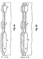
- heater board 20 includes an electrically-insulated silicon substrate 27 with a major surface 28 on which there is patterned CMOS drive circuitry 16 and channel stops 30.
- drive circuitry 16 could be fabricated using other fabrication techniques.
- Major surface 28, drive circuitry 16, and channel stops 30 are covered by a passivation layer 32, which consists of a 1 f..lm thick layer of silicon dioxide.
- passivation layer 32 On the top surface of passivation layer 32 there are patterned heater resistors 14, addressing electrodes 18, a power bus 34 for supplying power to resistors 14, and terminals 36 connected to addressing electrodes 18 and power bus 34, and aluminum interconnects 38.
- Aluminum interconnects 38 connect heating resistors 14 to power bus 34, and connect drive circuitry 16 to respective addressing electrodes 18 and respective heating resistors 14.
- each resistor 14 has ends 56 that abut its respective contact regions 54, and ends 56 lie beneath and approximately coincident with edges 58 of the portion of the top surface of tantalum regions 46 not covered by passivation layer 48. In this manner, resistors 14 are separated from the ink only by silicon oxide regions 42, silicon nitride regions 44 and tantalum regions 46.
- Field oxide regions 60 are constructed in the same steps used to fabricate channel stops 30. In this manner, field oxide regions 60 are constructed without adding any steps to the conventional CMOS fabrication process, or other conventional fabrication process used to fabricate drive circuitry 16.
- Passivation layer 32 includes three separate layers, a middle layer 62 doped with phosphorus, a non-doped underglaze 64, and non-doped overglaze mesas 66.
- Middle layer 62 is doped with phosphorus to facilitate reflow of middle layer 62.
- Underglaze 64 is positioned below, in contact and coextensive with, middle layer 62, and above drive circuitry 16 and field oxide regions 60. Underglaze 64 prevents phosphorus from middle doped layer 62 from diffusing to drive circuitry 16 and altering the electrical characteristics, particularly the electrical characteristics in the drift regions (not shown).
- One overglaze mesa 66 is positioned between middle layer 62 and resistors 14. Overglaze mesas 66 prevent phosphorus from middle layer 62 from diffusing to resistors 14 and altering their electrical characteristics.
- middle layer 62, underglaze 64 and mesas 66 could be used by themselves to provide a reliable printhead 10.
Applications Claiming Priority (2)
| Application Number | Priority Date | Filing Date | Title |
|---|---|---|---|
| US54756790A | 1990-07-02 | 1990-07-02 | |
| US547567 | 2000-04-12 |
Publications (2)
| Publication Number | Publication Date |
|---|---|
| EP0465212A2 true EP0465212A2 (fr) | 1992-01-08 |
| EP0465212A3 EP0465212A3 (en) | 1992-11-25 |
Family
ID=24185172
Family Applications (1)
| Application Number | Title | Priority Date | Filing Date |
|---|---|---|---|
| EP19910305984 Withdrawn EP0465212A3 (en) | 1990-07-02 | 1991-07-02 | Ink jet printheads |
Country Status (3)
| Country | Link |
|---|---|
| EP (1) | EP0465212A3 (fr) |
| JP (1) | JPH04232751A (fr) |
| CA (1) | CA2044402A1 (fr) |
Citations (4)
| Publication number | Priority date | Publication date | Assignee | Title |
|---|---|---|---|---|
| US4532530A (en) * | 1984-03-09 | 1985-07-30 | Xerox Corporation | Bubble jet printing device |
| US4719477A (en) * | 1986-01-17 | 1988-01-12 | Hewlett-Packard Company | Integrated thermal ink jet printhead and method of manufacture |
| US4935752A (en) * | 1989-03-30 | 1990-06-19 | Xerox Corporation | Thermal ink jet device with improved heating elements |
| EP0396315A1 (fr) * | 1989-05-01 | 1990-11-07 | Xerox Corporation | Tête d'impression thermique à jet d'encre avec des éléments chauffants générant des bulles |
-
1991
- 1991-06-12 CA CA 2044402 patent/CA2044402A1/fr not_active Abandoned
- 1991-07-02 JP JP16122591A patent/JPH04232751A/ja not_active Withdrawn
- 1991-07-02 EP EP19910305984 patent/EP0465212A3/en not_active Withdrawn
Patent Citations (4)
| Publication number | Priority date | Publication date | Assignee | Title |
|---|---|---|---|---|
| US4532530A (en) * | 1984-03-09 | 1985-07-30 | Xerox Corporation | Bubble jet printing device |
| US4719477A (en) * | 1986-01-17 | 1988-01-12 | Hewlett-Packard Company | Integrated thermal ink jet printhead and method of manufacture |
| US4935752A (en) * | 1989-03-30 | 1990-06-19 | Xerox Corporation | Thermal ink jet device with improved heating elements |
| EP0396315A1 (fr) * | 1989-05-01 | 1990-11-07 | Xerox Corporation | Tête d'impression thermique à jet d'encre avec des éléments chauffants générant des bulles |
Also Published As
| Publication number | Publication date |
|---|---|
| EP0465212A3 (en) | 1992-11-25 |
| CA2044402A1 (fr) | 1992-01-03 |
| JPH04232751A (ja) | 1992-08-21 |
Similar Documents
| Publication | Publication Date | Title |
|---|---|---|
| EP0154515B1 (fr) | Imprimante à projection d'encre par bulles | |
| JP4332227B2 (ja) | 熱式インク・ジェット・プリンタ用薄膜駆動ヘッド | |
| EP1326279B1 (fr) | Transistor à couche mince utilisé comme élément chauffant pour une chambre de microréaction | |
| US4774530A (en) | Ink jet printhead | |
| EP0434946B1 (fr) | Tête d'impression à jet d'encre avec passivation ionique des circuits électriques | |
| JP6878743B2 (ja) | サーマルインクジェット印字ヘッドを形成するための方法、サーマルインクジェット印字ヘッド、及び半導体ウエハ | |
| JPH09174851A (ja) | チップ内の熱障壁としてフィールド酸化物を具備する印刷ヘッド | |
| US8651604B2 (en) | Printheads | |
| EP0438295B1 (fr) | Têtes d'impression à jet d'encre thermiques | |
| US4835553A (en) | Thermal ink jet printhead with increased drop generation rate | |
| EP1352744B1 (fr) | Distributeur de liquide et imprimante | |
| EP0594369B1 (fr) | Agencement des éléments chauffants pour imprimante thermique par jet d'encre | |
| US20060121747A1 (en) | Ink-jet printhead fabrication | |
| EP1205303B1 (fr) | Imprimante, tête d'imprimante et procédé de fabrication de la tête d'imprimante | |
| US6132032A (en) | Thin-film print head for thermal ink-jet printers | |
| EP0465212A2 (fr) | Têtes d'imprimante à jet d'encre | |
| JP3584752B2 (ja) | 液体噴射記録装置およびその製造方法 | |
| KR19990063906A (ko) | 잉크 젯 프린팅 헤드 및 그 제조 방법 | |
| JP4137257B2 (ja) | サーマルインクジェットプリントヘッド及びその製造方法 | |
| US20030210301A1 (en) | Polysilicon feed-through fluid drop ejector | |
| KR100472485B1 (ko) | 잉크젯 프린트헤드 및 그 제조방법 | |
| US5969392A (en) | Thermal ink jet printheads with power MOS driver devices having enhanced transconductance | |
| CN100594131C (zh) | 喷墨头芯片结构 | |
| CN110406258B (zh) | 液体喷头基板、制造液体喷头基板的方法和液体喷头 | |
| KR100497368B1 (ko) | 잉크젯 프린트헤드 및 그 제조방법 |
Legal Events
| Date | Code | Title | Description |
|---|---|---|---|
| PUAI | Public reference made under article 153(3) epc to a published international application that has entered the european phase |
Free format text: ORIGINAL CODE: 0009012 |
|
| AK | Designated contracting states |
Kind code of ref document: A2 Designated state(s): DE FR GB |
|
| PUAL | Search report despatched |
Free format text: ORIGINAL CODE: 0009013 |
|
| AK | Designated contracting states |
Kind code of ref document: A3 Designated state(s): DE FR GB |
|
| STAA | Information on the status of an ep patent application or granted ep patent |
Free format text: STATUS: THE APPLICATION HAS BEEN WITHDRAWN |
|
| 18W | Application withdrawn |
Withdrawal date: 19930406 |