EP0460431A1 - A method of and an equipment for optical inspection of strip and sheet products - Google Patents
A method of and an equipment for optical inspection of strip and sheet products Download PDFInfo
- Publication number
- EP0460431A1 EP0460431A1 EP91107806A EP91107806A EP0460431A1 EP 0460431 A1 EP0460431 A1 EP 0460431A1 EP 91107806 A EP91107806 A EP 91107806A EP 91107806 A EP91107806 A EP 91107806A EP 0460431 A1 EP0460431 A1 EP 0460431A1
- Authority
- EP
- European Patent Office
- Prior art keywords
- signal
- value
- surface defects
- digital signal
- compression
- Prior art date
- Legal status (The legal status is an assumption and is not a legal conclusion. Google has not performed a legal analysis and makes no representation as to the accuracy of the status listed.)
- Granted
Links
Images

Classifications
-
- G—PHYSICS
- G01—MEASURING; TESTING
- G01N—INVESTIGATING OR ANALYSING MATERIALS BY DETERMINING THEIR CHEMICAL OR PHYSICAL PROPERTIES
- G01N21/00—Investigating or analysing materials by the use of optical means, i.e. using sub-millimetre waves, infrared, visible or ultraviolet light
- G01N21/84—Systems specially adapted for particular applications
- G01N21/88—Investigating the presence of flaws or contamination
- G01N21/89—Investigating the presence of flaws or contamination in moving material, e.g. running paper or textiles
- G01N21/8901—Optical details; Scanning details
- G01N21/8903—Optical details; Scanning details using a multiple detector array
-
- G—PHYSICS
- G06—COMPUTING; CALCULATING OR COUNTING
- G06T—IMAGE DATA PROCESSING OR GENERATION, IN GENERAL
- G06T9/00—Image coding
Definitions
- the present invention relates to a method of and an equipment for optical inspection of strip and sheet products for the detection of surface defects, which method comprises producing images of successive parts of the surface of a product, converting the images produced to an analog signal on the basis of the brightness of pixels, converting the analog signal to a digital signal by providing each pixel with a digital value representing its brightness, analyzing the digital signal for the detection of surface defects on the product and giving information of the surface defects detected.
- the object of the present invention is to provide a method and an equipment by means of which it is possible either to increase the inspection capacity or, alternatively, to simplify the equiment carrying out the inspection, without the quality of the inspection suffering therefrom, however.
- This is achieved by means of the method of the invention, which is characterized in that it further comprises compressing the digital signal before an analysis thereof.
- This compression can take place in such a manner that the value of each pixel is compared with n/2 preceding and n/2 following pixel values and it is replaced by the minimum or the maximum value observed at the comparison, depending on whether the surface defects show dark or light from the surroundings, and every nth value is selected from the sequence of values obtained in this way to be used for the production of the compressed signal.
- the pixels are divided at the compression into groups of n successive pixels and from each group is each time selected the one of the maximum or the minimum value, depending on whether the surface defects show dark or light from the surroundings, to be used for the production of the compressed signal.
- From a group of n successive pixels is preferably selected the one of the minimum or the maximum value by at first comparing the two first pixels with each other and by selecting from them the smaller/greater one and by comparing this with the following pixel and by selecting from them the smaller/greater one, and so on, the result of the comparison with the last pixel of the group being the pixel of the minimum or the maximum value searched for.
- an original signal is replaced by a signal containing the most substantial features of the original signal. It is thus certain that also the compressed signal includes all the information substantial for the inspection. If the compression is effected in the direction of pixel lines transverse to the strip, the information of the real width of a surface defect is lost at the compression. This width is, however, of no significance for the detection of a surface defect or even for the classification thereof. If the method is applied both in the transverse and the longitudinal direction of the strip, the information of the length of surface defects is also lost, which makes the classification of surface defects more difficult. Consequently, such a two-dimensional compression is not necessarily desirable, though possible.
- the equipment of the invention for optical inspection of strip and sheet products for the detection of surface defects comprises an image forming apparatus for producing images of successive parts of the surface of a product and for converting these images to an analog signal, an A/D converter for converting the analog signal to a digital signal and an image analyzing unit for an analysis of the digital signal in order to detect surface defects and to bring them to the user's knowledge.
- This equipment is characterized in that it further comprises a compression unit arranged between the A/D converter and the image analyzing unit for the compression of the digital signal before it is analyzed.
- the compression unit comprises n delay elements connected in series and n reference units connected in series and a register arranged after the nth reference unit, the series connection of the delay elements being arranged to receive the output signal of the A/D converter and the series connection of the reference units also being arranged to receive the output signal of the A/D converter, while each reference unit additionally receives the output signal of the corresponding delay element in order, and the register being arranged to deliver every nth signal value to its output.
- the compression unit comprises a series connection of a multiplexer, a delay element and a register, the multiplexer being arranged to receive the digital signal coming from the A/D converter and the output signal of the delay element, and a comparator arranged to receive the signal coming from the A/D converter and the output signal of the delay element, to compare these with each other and to control the multiplexer on the basis of the result of the comparison and a control logic arranged to control the register to deliver every nth signal value to its output and the comparator to control, irrespective of the comparison carried out thereby, the multiplexer to deliver every n+1st signal value to its output.
- Figure 1 shows the influence of a compression used in the optical inspection method according to the invention on the information to be processed.
- the upper example of Figure 1 presents a case in which the brightness of some pixel is substantially lower than that of the others, i.e. the strip to be inspected shows a dark area at this point.
- this tone profile at first is applied the alternative of the method of the invention, according to which the value of each pixel is compared with n/2 preceding and n/2 following pixel values and it is replaced by the minimum value observed at the comparison, a tone profile similar to that shown in Figure 1 under the title "tone profile of a filtered image" is obtained, in which tone profile n pixels have the same tone value as the pixel of the lowest tone value of the original image line.
- tone profile shown to the right in Figure 1 under the title "tone profile of a compressed image” is obtained, which tone profile substantially corresponds to the original tone profile, even if the number of pixels included in this tone profile only is the nth part of the number of pixels of the original tone profile. Thus is observed that no substantial information is lost in connection with an individual surface defect.
- the lower example of Figure 1 presents a case in which there are several surface defects within a short area.
- a tone profile is obtained in which all n pixels have been provided with the tone value of the pixel of the lowest tone value.
- This tone profile is shown in the middle part of Figure 1.
- the tone profile shown to the right in Figure 1 is obtained. Further, from this tone profile can reliably be seen the existence of a surface defect, but in this tone profile, however, several original surface defects have been united into one surface defect. Thus, the information of the width of the original surface defect has been lost at the compression.
- n can be some integer, for instance within the range 4 to 32, even if very high values of n are not necessarily advantageous when the compressed image shall be examined also visually, e.g. by means of a television monitor.
- Figure 2 shows an equipment for the realization of a method as described in Figure 1.
- the equipment comprises an image forming apparatus consisting of a video camera 1 of line or matrix type and an illumination device 2 for the illumination of a surface 3 to be inspected.
- images are produced of successive parts of the surface and converted to an analog video signal 4.
- This analog video signal is analog/digital converted by means of an A/D converter 5 to obtain a digital signal 6.
- this digital signal 6 is compressed by means of a unit 8 to obtain a compressed signal 9 before the signal is analyzed by means of an image analyzing unit 7.
- This image analyzing unit 7 comprises an image memory 14, an image processor 15 and a micro computer 16 connected in series.
- image analyzing units planned to be used for processing an uncompressed signal can be used.
- image analyzing units it is possible, firstly, to detect deviations to be interpreted as surface defects from the compressed digital signal 9 and, secondly, to provide the necessary alarms and reports on the inspection of the strip.
- An image analyzing unit like this is marketed for instance by Rautaruukki Oy with the designation SMARTVIS. Because this image analyzing unit is conventional per se and does not constitute a special object of the present invention, it will not be described in greater detail in this connection.
- the invention is formed by the image signal compression unit 8.
- this compression unit 8 comprises four delay elements 10 connected in series and four reference units 11 connected in series, respectively, and a register 12 for picking every 4th pixel from the digital signal fed thereto.
- the delay of each delay element 10 corresponds to one clock cycle of a clock CLK coming to the analog/digital converter 5.
- the series connection of the delay elements 10 relates to the series connection of the reference units 11 in such a way that to each reference unit is fed, firstly, a signal 19 of the preceding reference unit, and secondly, an output signal 13 of the delay element 10 with the corresponding order number.
- This reference unit selects from these two input signals either the smaller or the greater one, depending on whether the surface defects in this case show light or dark from the surroundings. This selected value is then fed by the reference unit 11 to the output 19 thereof. In this manner, each signal starting from the output of the last reference unit 11 has the value of the pixel of the minimum or the maximum value found among the values of 4 successive pixels, as has been described with reference to Figure 1.
- These successive values in digital form are then fed to the register 12 clocked with a clock frequency CLK/n, which in the example of Figure 2 is CLK/4, the digital signal 9 to be obtained from its output containing every 4th digital value from the sequence of values fed into the register 12.
- the image signal has been compressed to a form containing a quarter of the number of pixels included in the original digital signal 6.
- the image analyzing unit 7 can be realized either by means of equipments slower and thus simplier than before or by means of a conventional image analyzing unit, which now makes it possible to inspect an area 4 times wider than previously per time unit.
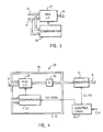
- FIG 3 shows the structure of the reference unit 11 included in the block diagram of Figure 2 in greater detail.
- This reference unit comprises a multiplexer 17 and a comparator 18. These two receive both the digital signal 13 coming from the delay element 10 and the digital signal 6, if it is the first comparator, or the output signal 19 of the preceding comparator.
- the comparator 18 compares these values with each other and selects from them either the greater or the smaller one, depending on whether a pixel of the lowest or the highest value is searched for.
- the comparator 18 controls the multiplexer 17, which has stored both in its input signal, in such a way that the value found on the basis of this comparison is brought to the output 19 of the multiplexer.
- the multiplexer 17 is of type 2:1, receiving two simultaneous input signals and delivering only one of them forward.
- Figure 4 shows a compression unit 20 suitable for being used instead of the compression unit 8 of Figure 2 and more easily realizable as an integrated circuit than the compression unit 8 shown in Figure 2, especially when the value of n increases. It is a fact that the number of both delay elements and reference units in the structure of Figure 2 is equal to n, while the number of components in the structure of Figure 4 does not need to be changed according to the value of n, but only the manner in which the circuit is controlled.
- the compression unit 20 of Figure 4 receives the digital signal 6 to be obtained from the analog/digital converter 5. At its output, it delivers the compressed digital signal 9 corresponding to the compressed digital signal 9 to be obtained in the embodiment of Figure 2.
- the compression unit 20 comprises a series connection of a multiplexer 21, a delay element 22 and a register 12, as well as a comparator 23 arranged to control the multiplexer 21.
- the register 12 corresponds substantially to the register 12 included in the compression unit 8 of Figure 2.
- the multiplexer 21 receives both the digital signal 6 and a signal 25 fed back from the output of this multiplexer 21 through the delay element 22.
- the comparator 23 receives also the digital signal 6 and the output signal 25 of the delay element 22.
- This comparator 23 selects from these inputs the greater or the smaller one, depending on whether the surface defects show dark or light against the background, and controls the multiplexer 21 on the basis of the result of the comparison by delivering to its output the value selected on the basis of the selection of the comparator 23.
- This value is brought to the delay element 22, the delay of which corresponds to one clock cycle.
- the output 25 of this delay element 22 is brought besides to the multiplexer 21 and the comparator 23 mentioned above also to the register 12, which is controlled by means of a control logic 24 to deliver every nth signal value to its output 9.
- This control logic 24 controls also the comparator 23 in such a way that the multiplexer 21 can be made to deliver to its output, irrespective of the result of the comparison, the value of the first pixel from a group each including n pixels, irrespective of the value of the last pixel of the preceding group including n pixels.
- the compression unit of Figure 4 performs a measure, in which the pixels are divided into groups of n successive pixels and from each group is in each particular case selected the one of the maximum or the minimum value, depending on whether the surface defects show dark or light from their surroundings.
- this minimum or maximum pixel from a group of n successive pixels is selected by at first comparing the two first pixels with each other and by selecting from them the smaller/greater one and by comparing this with next pixel and by selecting from them the smaller/greater one, and so on, the result of the comparison carried out with the last, i.e. the nth, pixel of the group being the pixel of the minimum or the maximum value from this group of n pixels searched for.
- the two-dimensional area of the surface to be inspected could now be represented by means of one pixel.
- Such a two-dimensional compression is, however, out of the question, if a loss of information about the real range of a surface defect is not desired in either direction of compression.
Abstract
Description
- The present invention relates to a method of and an equipment for optical inspection of strip and sheet products for the detection of surface defects, which method comprises
producing images of successive parts of the surface of a product,
converting the images produced to an analog signal on the basis of the brightness of pixels,
converting the analog signal to a digital signal by providing each pixel with a digital value representing its brightness,
analyzing the digital signal for the detection of surface defects on the product and
giving information of the surface defects detected. - A method of detecting surface defects on a moving strip, similar to the one described above, is known from U.S. Patent 4 665 317. By means of such an equipment, it is possible to alarm the operating personnel when substantial surface defects appear, and moreover, to produce necessary inspection reports. An introduction of automatic inspection equipments like this has been based firstly on the fact that it is problematic to get manpower capable enough of doing this kind of work of a very monotonous nature, and secondly on the fact that an inspection carried out by a man is not at all possible any more when the strip speeds are increasing. The increased strip speeds and also the desire to provide an image as detailed as possible of the defects possibly occurring on the strip create a need to increase also the processing capacity of the automatic inspection equipment. The problem will then be the number of the operations needed. The fact is that if a 1500 mm broad strip moving at the speed of 300 m/min is inspected with the image dot size being 1 mm, the system shall be capable of analyzing 7,5 millions of image dots per second. In practice, it is possible to provide without excessive costs an equipment capable of doing 1,5 milliards of image dot operations per second. However, such a speed requires already that relatively expensive equipments are used. If a further increase of the capacity of the equipment were desired, it would be necessary to acquire several equipments like this expensive as such and to place them adjacent to each other, each equipment arranged to inspect only a part of the strip width.
- The object of the present invention is to provide a method and an equipment by means of which it is possible either to increase the inspection capacity or, alternatively, to simplify the equiment carrying out the inspection, without the quality of the inspection suffering therefrom, however. This is achieved by means of the method of the invention, which is characterized in that it further comprises compressing the digital signal before an analysis thereof.
- This compression can take place in such a manner that the value of each pixel is compared with n/2 preceding and n/2 following pixel values and it is replaced by the minimum or the maximum value observed at the comparison, depending on whether the surface defects show dark or light from the surroundings, and every nth value is selected from the sequence of values obtained in this way to be used for the production of the compressed signal.
- Alternatively, the pixels are divided at the compression into groups of n successive pixels and from each group is each time selected the one of the maximum or the minimum value, depending on whether the surface defects show dark or light from the surroundings, to be used for the production of the compressed signal. From a group of n successive pixels is preferably selected the one of the minimum or the maximum value by at first comparing the two first pixels with each other and by selecting from them the smaller/greater one and by comparing this with the following pixel and by selecting from them the smaller/greater one, and so on, the result of the comparison with the last pixel of the group being the pixel of the minimum or the maximum value searched for.
- At an image signal compression effected by methods of the kind described above, an original signal is replaced by a signal containing the most substantial features of the original signal. It is thus certain that also the compressed signal includes all the information substantial for the inspection. If the compression is effected in the direction of pixel lines transverse to the strip, the information of the real width of a surface defect is lost at the compression. This width is, however, of no significance for the detection of a surface defect or even for the classification thereof. If the method is applied both in the transverse and the longitudinal direction of the strip, the information of the length of surface defects is also lost, which makes the classification of surface defects more difficult. Consequently, such a two-dimensional compression is not necessarily desirable, though possible.
- The equipment of the invention for optical inspection of strip and sheet products for the detection of surface defects comprises an image forming apparatus for producing images of successive parts of the surface of a product and for converting these images to an analog signal, an A/D converter for converting the analog signal to a digital signal and an image analyzing unit for an analysis of the digital signal in order to detect surface defects and to bring them to the user's knowledge. This equipment is characterized in that it further comprises a compression unit arranged between the A/D converter and the image analyzing unit for the compression of the digital signal before it is analyzed.
- According to a first embodiment of the invention, the compression unit comprises n delay elements connected in series and n reference units connected in series and a register arranged after the nth reference unit, the series connection of the delay elements being arranged to receive the output signal of the A/D converter and the series connection of the reference units also being arranged to receive the output signal of the A/D converter, while each reference unit additionally receives the output signal of the corresponding delay element in order, and the register being arranged to deliver every nth signal value to its output.
- According to a second embodiment of the invention, being especially advantageous with respect to a realization of the invention as an integrated circuit, the compression unit comprises a series connection of a multiplexer, a delay element and a register, the multiplexer being arranged to receive the digital signal coming from the A/D converter and the output signal of the delay element, and a comparator arranged to receive the signal coming from the A/D converter and the output signal of the delay element, to compare these with each other and to control the multiplexer on the basis of the result of the comparison and a control logic arranged to control the register to deliver every nth signal value to its output and the comparator to control, irrespective of the comparison carried out thereby, the multiplexer to deliver every n+1st signal value to its output.
- In the following, the method and the equipment of the invention are described in greater detail referring to the enclosed drawing, in which
- Figure 1 shows a change in the tone profile of an image line in connection with a compression according to the invention,
- Figure 2 shows a block diagram of an equipment according to a first embodiment of the invention,
- Figure 3 shows the structure of a reference unit included in the equipment of Figure 2 in greater detail, and
- Figure 4 shows a block diagram of a compression unit included in an equipment of a second embodiment of the invention.
- Figure 1 shows the influence of a compression used in the optical inspection method according to the invention on the information to be processed. The upper example of Figure 1 presents a case in which the brightness of some pixel is substantially lower than that of the others, i.e. the strip to be inspected shows a dark area at this point. When to this tone profile at first is applied the alternative of the method of the invention, according to which the value of each pixel is compared with n/2 preceding and n/2 following pixel values and it is replaced by the minimum value observed at the comparison, a tone profile similar to that shown in Figure 1 under the title "tone profile of a filtered image" is obtained, in which tone profile n pixels have the same tone value as the pixel of the lowest tone value of the original image line. When every nth value is then picked according to the invention from this tone profile, a tone profile shown to the right in Figure 1 under the title "tone profile of a compressed image" is obtained, which tone profile substantially corresponds to the original tone profile, even if the number of pixels included in this tone profile only is the nth part of the number of pixels of the original tone profile. Thus is observed that no substantial information is lost in connection with an individual surface defect.
- The lower example of Figure 1 presents a case in which there are several surface defects within a short area. When the above procedure is applied to this tone profile, a tone profile is obtained in which all n pixels have been provided with the tone value of the pixel of the lowest tone value. This tone profile is shown in the middle part of Figure 1. When every nth value is then picked from this tone profile, the tone profile shown to the right in Figure 1 is obtained. Further, from this tone profile can reliably be seen the existence of a surface defect, but in this tone profile, however, several original surface defects have been united into one surface defect. Thus, the information of the width of the original surface defect has been lost at the compression. This width of the surface defect is, however, of no substantial significance for the detection of surface defects or for the classification thereof either, when a classification of surface defects on metal strips or sheets is concerned. In practical cases, n can be some integer, for instance within the range 4 to 32, even if very high values of n are not necessarily advantageous when the compressed image shall be examined also visually, e.g. by means of a television monitor.
- Figure 2 shows an equipment for the realization of a method as described in Figure 1. Firstly, the equipment comprises an image forming apparatus consisting of a
video camera 1 of line or matrix type and anillumination device 2 for the illumination of asurface 3 to be inspected. By means of this image forming apparatus, images are produced of successive parts of the surface and converted to an analog video signal 4. This analog video signal is analog/digital converted by means of an A/D converter 5 to obtain adigital signal 6. After this, thisdigital signal 6 is compressed by means of aunit 8 to obtain acompressed signal 9 before the signal is analyzed by means of animage analyzing unit 7. Thisimage analyzing unit 7 comprises an image memory 14, animage processor 15 and a micro computer 16 connected in series. Because the image is preserved in "image form" (matrix form) at the compression, without the structure of the image being broken or changed into a substantially different format, image analyzing units planned to be used for processing an uncompressed signal can be used. By means of such image analyzing units, it is possible, firstly, to detect deviations to be interpreted as surface defects from the compresseddigital signal 9 and, secondly, to provide the necessary alarms and reports on the inspection of the strip. An image analyzing unit like this is marketed for instance by Rautaruukki Oy with the designation SMARTVIS. Because this image analyzing unit is conventional per se and does not constitute a special object of the present invention, it will not be described in greater detail in this connection. - For the most substantial part, the invention is formed by the image
signal compression unit 8. In the exemplifying embodiment of Figure 2, thiscompression unit 8 comprises four delay elements 10 connected in series and fourreference units 11 connected in series, respectively, and aregister 12 for picking every 4th pixel from the digital signal fed thereto. The delay of each delay element 10 corresponds to one clock cycle of a clock CLK coming to the analog/digital converter 5. The series connection of the delay elements 10 relates to the series connection of thereference units 11 in such a way that to each reference unit is fed, firstly, asignal 19 of the preceding reference unit, and secondly, anoutput signal 13 of the delay element 10 with the corresponding order number. This reference unit then selects from these two input signals either the smaller or the greater one, depending on whether the surface defects in this case show light or dark from the surroundings. This selected value is then fed by thereference unit 11 to theoutput 19 thereof. In this manner, each signal starting from the output of thelast reference unit 11 has the value of the pixel of the minimum or the maximum value found among the values of 4 successive pixels, as has been described with reference to Figure 1. These successive values in digital form are then fed to theregister 12 clocked with a clock frequency CLK/n, which in the example of Figure 2 is CLK/4, thedigital signal 9 to be obtained from its output containing every 4th digital value from the sequence of values fed into theregister 12. In this way, the image signal has been compressed to a form containing a quarter of the number of pixels included in the originaldigital signal 6. So, theimage analyzing unit 7 can be realized either by means of equipments slower and thus simplier than before or by means of a conventional image analyzing unit, which now makes it possible to inspect an area 4 times wider than previously per time unit. - Figure 3 shows the structure of the
reference unit 11 included in the block diagram of Figure 2 in greater detail. This reference unit comprises amultiplexer 17 and acomparator 18. These two receive both thedigital signal 13 coming from the delay element 10 and thedigital signal 6, if it is the first comparator, or theoutput signal 19 of the preceding comparator. Thecomparator 18 compares these values with each other and selects from them either the greater or the smaller one, depending on whether a pixel of the lowest or the highest value is searched for. On the basis of the comparison, thecomparator 18 controls themultiplexer 17, which has stored both in its input signal, in such a way that the value found on the basis of this comparison is brought to theoutput 19 of the multiplexer. Thus themultiplexer 17 is of type 2:1, receiving two simultaneous input signals and delivering only one of them forward. - Figure 4 shows a
compression unit 20 suitable for being used instead of thecompression unit 8 of Figure 2 and more easily realizable as an integrated circuit than thecompression unit 8 shown in Figure 2, especially when the value of n increases. It is a fact that the number of both delay elements and reference units in the structure of Figure 2 is equal to n, while the number of components in the structure of Figure 4 does not need to be changed according to the value of n, but only the manner in which the circuit is controlled. - At its input, the
compression unit 20 of Figure 4 receives thedigital signal 6 to be obtained from the analog/digital converter 5. At its output, it delivers the compresseddigital signal 9 corresponding to the compresseddigital signal 9 to be obtained in the embodiment of Figure 2. Thecompression unit 20 comprises a series connection of amultiplexer 21, adelay element 22 and aregister 12, as well as acomparator 23 arranged to control themultiplexer 21. As appears from the reference numerals, theregister 12 corresponds substantially to theregister 12 included in thecompression unit 8 of Figure 2. In thecompression unit 20 of Figure 4, themultiplexer 21 receives both thedigital signal 6 and asignal 25 fed back from the output of thismultiplexer 21 through thedelay element 22. Thecomparator 23 receives also thedigital signal 6 and theoutput signal 25 of thedelay element 22. Thiscomparator 23 selects from these inputs the greater or the smaller one, depending on whether the surface defects show dark or light against the background, and controls themultiplexer 21 on the basis of the result of the comparison by delivering to its output the value selected on the basis of the selection of thecomparator 23. This value is brought to thedelay element 22, the delay of which corresponds to one clock cycle. Theoutput 25 of thisdelay element 22 is brought besides to themultiplexer 21 and thecomparator 23 mentioned above also to theregister 12, which is controlled by means of acontrol logic 24 to deliver every nth signal value to itsoutput 9. Thiscontrol logic 24 controls also thecomparator 23 in such a way that themultiplexer 21 can be made to deliver to its output, irrespective of the result of the comparison, the value of the first pixel from a group each including n pixels, irrespective of the value of the last pixel of the preceding group including n pixels. In this manner, the compression unit of Figure 4 performs a measure, in which the pixels are divided into groups of n successive pixels and from each group is in each particular case selected the one of the maximum or the minimum value, depending on whether the surface defects show dark or light from their surroundings. In thecompression unit 20, this minimum or maximum pixel from a group of n successive pixels is selected by at first comparing the two first pixels with each other and by selecting from them the smaller/greater one and by comparing this with next pixel and by selecting from them the smaller/greater one, and so on, the result of the comparison carried out with the last, i.e. the nth, pixel of the group being the pixel of the minimum or the maximum value from this group of n pixels searched for. - Two exemplifying methods and equipments have been described above for carrying out a desired compression of a digital image signal. It is understandable that the same result can be provided also in manners somewhat deviating from the procedures or structural solutions described above, without deviating from the scope of protection defined by the enclosed claims, however. Additionally, the methods and equipments described above could further be complemented by parts capable of providing a two-dimensional compression of the image signal, to which has been referred already in some degree. Such a compression could be realized by collecting to a suitable memory a sufficient number of compressed
digital signals 9 and by performing a new compression of these signals in such a manner that the compression would now be effected by comparing each compressed pixel with adjacent pixels seen in the longitudinal direction of the strip. Thus, the two-dimensional area of the surface to be inspected could now be represented by means of one pixel. Such a two-dimensional compression is, however, out of the question, if a loss of information about the real range of a surface defect is not desired in either direction of compression.
Claims (7)
- A method of optical inspection of strip and sheet products for the detection of surface defects, which method comprises
producing images of successive parts of the surface of a product,
converting the images produced to an analog signal on the basis of the brightness of pixels,
converting the analog signal to a digital signal by providing each pixel with a digital value representing its brightness,
analyzing the digital signal for the detection of surface defects on the product and
giving information of the surface defects detected, characterized in that the method further comprises compressing the digital signal before an analysis thereof. - A method according to claim 1, characterized in that at the compression the value of each pixel is compared with n/2 preceding and n/2 following pixel values and it is replaced by the minimum or the maximum value observed at the comparison, depending on whether the surface defects show dark or light from the surroundings, and every nth value is selected from the sequence of values obtained in this way to be used for the production of the compressed signal.
- A method according to claim 1, characterized in that at the compression the pixels are divided into groups of n successive pixels and from each group is each time selected the one of the maximum or the minimum value, depending on whether the surface defects show dark or light from their surroundings, to be used for the production of the compressed signal.
- A method according to claim 3, characterized in that from a group of n successive pixels is selected the one of the minimum or the maximum value by at first comparing the two first pixels with each other and by selecting from them the smaller/greater one and by comparing this with the following pixel and by selecting from them the smaller/greater one, and so on, the result of the comparison with the last pixel of the group being the pixel of the minimum or the maximum value searched for.
- An equipment for optical inspection of strip and sheet products for the detection of surface defects, comprising an image forming apparatus (1, 2) for the production of images of successive parts of the surface of a product (3) and for the conversion of these images to an analog signal (4), an A/D converter (5) for the conversion of the analog signal (4) to a digital signal (6) and an image analyzing unit (7) for analyzing the digital signal (6) in order to detect surface defects and to bring them to the user's knowledge, characterzed in that the equipment further comprises a compression unit (8; 20) arranged between the A/D converter (5) and the image analyzing unit (7) for the compression of the digital signal (6) before it is analyzed.
- An equipment according to claim 5, characterized in that the compression unit (8) comprises n delay units (10) connected in series and n reference units (11) connected in series and a register (12) arranged after the nth reference unit, the series connection of the delay elements (10) being arranged to receive the output signal (6) of the A/D converter (5) and the series connection of the reference units (11) being in the same way arranged to receive the output signal (6) of the A/D converter (5), while each reference unit (11) additionally receives an output signal (13) of the corresponding delay unit (10) in order and the register (12) being arranged to deliver every nth signal value to its output.
- An equipment according to claim 5, characterized in that the compression unit (20) comprises a series connection of a multiplexer (21), a delay element (22) and a register (12), the multiplexer (21) being arranged to receive the digital signal (6) coming from the A/D converter (5) and an output signal (25) of the delay element (22), and a comparator (23) arranged to receive the signal (6) coming from the A/D converter (5) and the output signal (25) of the delay element (22), to compare these with each other and to control the multiplexer (21) on the basis of the result of the comparison, and a control logic (24) arranged to control the register (12) to deliver every nth signal value to its output (9) and the comparator (23) to control, irrespective of the comparison performed by it, the multiplexer (21) to deliver every n+1st signal value to its output.
Applications Claiming Priority (2)
| Application Number | Priority Date | Filing Date | Title |
|---|---|---|---|
| FI902842 | 1990-06-07 | ||
| FI902842A FI85308C (en) | 1990-06-07 | 1990-06-07 | Method and apparatus for optical examination of sheet and web-shaped products |
Publications (2)
| Publication Number | Publication Date |
|---|---|
| EP0460431A1 true EP0460431A1 (en) | 1991-12-11 |
| EP0460431B1 EP0460431B1 (en) | 1994-11-02 |
Family
ID=8530584
Family Applications (1)
| Application Number | Title | Priority Date | Filing Date |
|---|---|---|---|
| EP91107806A Expired - Lifetime EP0460431B1 (en) | 1990-06-07 | 1991-05-14 | A method of and an equipment for optical inspection of strip and sheet products |
Country Status (7)
| Country | Link |
|---|---|
| US (1) | US5263094A (en) |
| EP (1) | EP0460431B1 (en) |
| JP (1) | JPH04232573A (en) |
| AT (1) | ATE113719T1 (en) |
| CA (1) | CA2041456A1 (en) |
| DE (1) | DE69104906T2 (en) |
| FI (1) | FI85308C (en) |
Cited By (4)
| Publication number | Priority date | Publication date | Assignee | Title |
|---|---|---|---|---|
| EP0465233A2 (en) * | 1990-07-06 | 1992-01-08 | Westinghouse Electric Corporation | Vision inspection systems |
| EP0543629A1 (en) * | 1991-11-19 | 1993-05-26 | E.I. Du Pont De Nemours And Company | Defect detection |
| GB2272764A (en) * | 1992-11-24 | 1994-05-25 | Rheimetall Sick Optical Inspec | Inspecting surfaces of materials by optical scanning |
| EP0823629A2 (en) * | 1996-08-05 | 1998-02-11 | Chep Pooling Systems BV | Process for the automatic recognition and categorization of defects in pallets or similar elements, and corresponding system |
Families Citing this family (8)
| Publication number | Priority date | Publication date | Assignee | Title |
|---|---|---|---|---|
| US5515452A (en) * | 1992-12-31 | 1996-05-07 | Electroglas, Inc. | Optical character recognition illumination method and system |
| US6064429A (en) * | 1997-08-18 | 2000-05-16 | Mcdonnell Douglas Corporation | Foreign object video detection and alert system and method |
| US7171033B2 (en) * | 2001-03-28 | 2007-01-30 | The Boeing Company | System and method for identifying defects in a composite structure |
| US6871684B2 (en) | 2002-08-13 | 2005-03-29 | The Boeing Company | System for identifying defects in a composite structure |
| US7424902B2 (en) | 2004-11-24 | 2008-09-16 | The Boeing Company | In-process vision detection of flaw and FOD characteristics |
| US20060108048A1 (en) * | 2004-11-24 | 2006-05-25 | The Boeing Company | In-process vision detection of flaws and fod by back field illumination |
| SE0702163L (en) * | 2007-09-25 | 2008-12-23 | Abb Research Ltd | An apparatus and method for stabilizing and visual monitoring an elongated metallic band |
| TWI387320B (en) * | 2008-08-15 | 2013-02-21 | Novatek Microelectronics Corp | Apparatus and method for filtering image signal noise |
Citations (6)
| Publication number | Priority date | Publication date | Assignee | Title |
|---|---|---|---|---|
| DE1762412A1 (en) * | 1968-06-12 | 1970-05-06 | Telefunken Patent | Device in a data processing system with an analog-digital conversion stage and a digital memory connected downstream of this |
| EP0225428A2 (en) * | 1985-11-30 | 1987-06-16 | ANT Nachrichtentechnik GmbH | Method for the recognition of edge structures in a picture signal |
| US4751572A (en) * | 1986-12-30 | 1988-06-14 | The United States Of America As Represented By The United States Department Of Energy | High speed data compactor |
| EP0311990A2 (en) * | 1987-10-15 | 1989-04-19 | Futec Incorporated | Method and apparatus for detecting disparity of cyclic length of printed patterns |
| US4908871A (en) * | 1986-04-21 | 1990-03-13 | Hitachi, Ltd. | Pattern inspection system |
| EP0368460A1 (en) * | 1988-09-29 | 1990-05-16 | Sony Corporation | Coding apparatus |
Family Cites Families (1)
| Publication number | Priority date | Publication date | Assignee | Title |
|---|---|---|---|---|
| FR2559581B1 (en) * | 1984-02-10 | 1986-07-11 | Siderurgie Fse Inst Rech | METHOD AND INSTALLATION FOR DETECTING SURFACE DEFECTS ON A TAPE DURING TRIPPING |
-
1990
- 1990-06-07 FI FI902842A patent/FI85308C/en not_active IP Right Cessation
-
1991
- 1991-04-29 CA CA002041456A patent/CA2041456A1/en not_active Abandoned
- 1991-05-14 AT AT91107806T patent/ATE113719T1/en not_active IP Right Cessation
- 1991-05-14 DE DE69104906T patent/DE69104906T2/en not_active Expired - Fee Related
- 1991-05-14 EP EP91107806A patent/EP0460431B1/en not_active Expired - Lifetime
- 1991-05-20 JP JP3143983A patent/JPH04232573A/en not_active Withdrawn
- 1991-05-28 US US07/705,621 patent/US5263094A/en not_active Expired - Fee Related
Patent Citations (6)
| Publication number | Priority date | Publication date | Assignee | Title |
|---|---|---|---|---|
| DE1762412A1 (en) * | 1968-06-12 | 1970-05-06 | Telefunken Patent | Device in a data processing system with an analog-digital conversion stage and a digital memory connected downstream of this |
| EP0225428A2 (en) * | 1985-11-30 | 1987-06-16 | ANT Nachrichtentechnik GmbH | Method for the recognition of edge structures in a picture signal |
| US4908871A (en) * | 1986-04-21 | 1990-03-13 | Hitachi, Ltd. | Pattern inspection system |
| US4751572A (en) * | 1986-12-30 | 1988-06-14 | The United States Of America As Represented By The United States Department Of Energy | High speed data compactor |
| EP0311990A2 (en) * | 1987-10-15 | 1989-04-19 | Futec Incorporated | Method and apparatus for detecting disparity of cyclic length of printed patterns |
| EP0368460A1 (en) * | 1988-09-29 | 1990-05-16 | Sony Corporation | Coding apparatus |
Cited By (8)
| Publication number | Priority date | Publication date | Assignee | Title |
|---|---|---|---|---|
| EP0465233A2 (en) * | 1990-07-06 | 1992-01-08 | Westinghouse Electric Corporation | Vision inspection systems |
| EP0465233A3 (en) * | 1990-07-06 | 1992-11-25 | Westinghouse Electric Corporation | Vision inspection systems |
| EP0543629A1 (en) * | 1991-11-19 | 1993-05-26 | E.I. Du Pont De Nemours And Company | Defect detection |
| GB2272764A (en) * | 1992-11-24 | 1994-05-25 | Rheimetall Sick Optical Inspec | Inspecting surfaces of materials by optical scanning |
| GB2272764B (en) * | 1992-11-24 | 1996-06-05 | Rheinmetall Sick Optical Inspe | Method and system for the inspection of the surfaces of materials |
| US5566243A (en) * | 1992-11-24 | 1996-10-15 | Rheinmetall Sick Optical Inspection Systems Gmbh | Method and apparatus for the inspection of surfaces |
| EP0823629A2 (en) * | 1996-08-05 | 1998-02-11 | Chep Pooling Systems BV | Process for the automatic recognition and categorization of defects in pallets or similar elements, and corresponding system |
| EP0823629A3 (en) * | 1996-08-05 | 1998-03-25 | Chep Pooling Systems BV | Process for the automatic recognition and categorization of defects in pallets or similar elements, and corresponding system |
Also Published As
| Publication number | Publication date |
|---|---|
| FI85308C (en) | 1992-03-25 |
| JPH04232573A (en) | 1992-08-20 |
| US5263094A (en) | 1993-11-16 |
| EP0460431B1 (en) | 1994-11-02 |
| FI902842A0 (en) | 1990-06-07 |
| FI902842A (en) | 1991-12-08 |
| ATE113719T1 (en) | 1994-11-15 |
| DE69104906T2 (en) | 1995-03-23 |
| FI85308B (en) | 1991-12-13 |
| DE69104906D1 (en) | 1994-12-08 |
| CA2041456A1 (en) | 1991-12-08 |
Similar Documents
| Publication | Publication Date | Title |
|---|---|---|
| US5263094A (en) | Method of and an equipment for optical inspection of strip and sheet products | |
| EP0844588A3 (en) | Image processing apparatus and method | |
| EP2199973A3 (en) | An image processing apparatus and method, and an image evaluation device and method | |
| US3908078A (en) | Method and apparatus for digital recognition of objects particularly biological materials | |
| JP3305819B2 (en) | Method and apparatus for monitoring image processing operations | |
| US5223932A (en) | Dynamic offset to increase the range of digitization of video images | |
| EP0367952A3 (en) | System for detecting and analyzing rounded objects | |
| CA2050711A1 (en) | High resolution camera sensor having a linear pixel array | |
| EP0094824B1 (en) | Image processing device for continuously extracting features of small regions of an image | |
| JPH06229941A (en) | Inspection apparatus for image | |
| KR20030013520A (en) | Image processing system | |
| JP2002195952A (en) | Surface flaw detecting device | |
| KR100311282B1 (en) | Automatic inspection system for quality of connection cable | |
| US5631468A (en) | Telecamera with a high frame frequency and associated manufacturing method | |
| US4750210A (en) | Method and apparatus for finding objects within a visual display | |
| JPH0829357A (en) | Appearance inspection device for automation line | |
| JP3149927B2 (en) | LOFAR gram display method and apparatus | |
| JPH03173291A (en) | Method for generating digital sign from video signal or tv transmitting frame | |
| JPS6118229B2 (en) | ||
| JPH09218957A (en) | Image processing method | |
| JP2513759B2 (en) | Video rate image processing method | |
| EP1229722A2 (en) | A method for imaging of manufacturing processes | |
| JPS63167978A (en) | Image processor | |
| JPH03252545A (en) | Wiring pattern inspection device | |
| JPH04299689A (en) | Picture processing device |
Legal Events
| Date | Code | Title | Description |
|---|---|---|---|
| PUAI | Public reference made under article 153(3) epc to a published international application that has entered the european phase |
Free format text: ORIGINAL CODE: 0009012 |
|
| AK | Designated contracting states |
Kind code of ref document: A1 Designated state(s): AT BE CH DE DK ES FR GB GR IT LI LU NL SE |
|
| 17P | Request for examination filed |
Effective date: 19920116 |
|
| 17Q | First examination report despatched |
Effective date: 19930719 |
|
| GRAA | (expected) grant |
Free format text: ORIGINAL CODE: 0009210 |
|
| AK | Designated contracting states |
Kind code of ref document: B1 Designated state(s): AT BE CH DE DK ES FR GB GR IT LI LU NL SE |
|
| PG25 | Lapsed in a contracting state [announced via postgrant information from national office to epo] |
Ref country code: IT Free format text: LAPSE BECAUSE OF FAILURE TO SUBMIT A TRANSLATION OF THE DESCRIPTION OR TO PAY THE FEE WITHIN THE PRE;WARNING: LAPSES OF ITALIAN PATENTS WITH EFFECTIVE DATE BEFORE 2007 MAY HAVE OCCURRED AT ANY TIME BEFORE 2007. THE CORRECT EFFECTIVE DATE MAY BE DIFFERENT FROM THE ONE RECORDED.SCRIBED TIME-LIMIT Effective date: 19941102 Ref country code: ES Free format text: THE PATENT HAS BEEN ANNULLED BY A DECISION OF A NATIONAL AUTHORITY Effective date: 19941102 Ref country code: CH Effective date: 19941102 Ref country code: DK Effective date: 19941102 Ref country code: AT Effective date: 19941102 Ref country code: NL Effective date: 19941102 Ref country code: GR Free format text: LAPSE BECAUSE OF FAILURE TO SUBMIT A TRANSLATION OF THE DESCRIPTION OR TO PAY THE FEE WITHIN THE PRESCRIBED TIME-LIMIT Effective date: 19941102 Ref country code: LI Effective date: 19941102 |
|
| REF | Corresponds to: |
Ref document number: 113719 Country of ref document: AT Date of ref document: 19941115 Kind code of ref document: T |
|
| REF | Corresponds to: |
Ref document number: 69104906 Country of ref document: DE Date of ref document: 19941208 |
|
| PG25 | Lapsed in a contracting state [announced via postgrant information from national office to epo] |
Ref country code: SE Effective date: 19950202 |
|
| REG | Reference to a national code |
Ref country code: CH Ref legal event code: PL |
|
| ET | Fr: translation filed | ||
| NLV1 | Nl: lapsed or annulled due to failure to fulfill the requirements of art. 29p and 29m of the patents act | ||
| PG25 | Lapsed in a contracting state [announced via postgrant information from national office to epo] |
Ref country code: LU Free format text: LAPSE BECAUSE OF NON-PAYMENT OF DUE FEES Effective date: 19950531 |
|
| PLBE | No opposition filed within time limit |
Free format text: ORIGINAL CODE: 0009261 |
|
| STAA | Information on the status of an ep patent application or granted ep patent |
Free format text: STATUS: NO OPPOSITION FILED WITHIN TIME LIMIT |
|
| 26N | No opposition filed | ||
| PGFP | Annual fee paid to national office [announced via postgrant information from national office to epo] |
Ref country code: FR Payment date: 19970529 Year of fee payment: 7 |
|
| PGFP | Annual fee paid to national office [announced via postgrant information from national office to epo] |
Ref country code: DE Payment date: 19970627 Year of fee payment: 7 |
|
| PG25 | Lapsed in a contracting state [announced via postgrant information from national office to epo] |
Ref country code: FR Free format text: LAPSE BECAUSE OF NON-PAYMENT OF DUE FEES Effective date: 19980531 |
|
| PGFP | Annual fee paid to national office [announced via postgrant information from national office to epo] |
Ref country code: BE Payment date: 19980604 Year of fee payment: 8 |
|
| PG25 | Lapsed in a contracting state [announced via postgrant information from national office to epo] |
Ref country code: DE Free format text: LAPSE BECAUSE OF NON-PAYMENT OF DUE FEES Effective date: 19990302 |
|
| REG | Reference to a national code |
Ref country code: FR Ref legal event code: ST |
|
| PG25 | Lapsed in a contracting state [announced via postgrant information from national office to epo] |
Ref country code: BE Free format text: LAPSE BECAUSE OF NON-PAYMENT OF DUE FEES Effective date: 19990531 |
|
| BERE | Be: lapsed |
Owner name: RAUTARUUKKI OY Effective date: 19990531 |
|
| PGFP | Annual fee paid to national office [announced via postgrant information from national office to epo] |
Ref country code: GB Payment date: 20010424 Year of fee payment: 11 |
|
| REG | Reference to a national code |
Ref country code: GB Ref legal event code: IF02 |
|
| PG25 | Lapsed in a contracting state [announced via postgrant information from national office to epo] |
Ref country code: GB Free format text: LAPSE BECAUSE OF NON-PAYMENT OF DUE FEES Effective date: 20020514 |
|
| GBPC | Gb: european patent ceased through non-payment of renewal fee |
Effective date: 20020514 |