EP0094824B1 - Image processing device for continuously extracting features of small regions of an image - Google Patents
Image processing device for continuously extracting features of small regions of an image Download PDFInfo
- Publication number
- EP0094824B1 EP0094824B1 EP83302764A EP83302764A EP0094824B1 EP 0094824 B1 EP0094824 B1 EP 0094824B1 EP 83302764 A EP83302764 A EP 83302764A EP 83302764 A EP83302764 A EP 83302764A EP 0094824 B1 EP0094824 B1 EP 0094824B1
- Authority
- EP
- European Patent Office
- Prior art keywords
- data
- memory means
- picture element
- image
- output data
- Prior art date
- Legal status (The legal status is an assumption and is not a legal conclusion. Google has not performed a legal analysis and makes no representation as to the accuracy of the status listed.)
- Expired
Links
Images

Classifications
-
- G—PHYSICS
- G06—COMPUTING; CALCULATING OR COUNTING
- G06T—IMAGE DATA PROCESSING OR GENERATION, IN GENERAL
- G06T7/00—Image analysis
-
- G—PHYSICS
- G01—MEASURING; TESTING
- G01N—INVESTIGATING OR ANALYSING MATERIALS BY DETERMINING THEIR CHEMICAL OR PHYSICAL PROPERTIES
- G01N21/00—Investigating or analysing materials by the use of optical means, i.e. using sub-millimetre waves, infrared, visible or ultraviolet light
- G01N21/84—Systems specially adapted for particular applications
- G01N21/88—Investigating the presence of flaws or contamination
- G01N21/89—Investigating the presence of flaws or contamination in moving material, e.g. running paper or textiles
Definitions
- the present invention relates to an image processing device and, more particularly, to an image processing device arranged to effectively extract the features of small areas of an image.
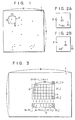
- an image 1 has (MxN) picture elements and is divided into small regions 2 each of (mxn) picture elements. It is also assumed that the image processing is performed to inspect the number of defects within the area of each divided region 2. For instance, it is also assumed that, a small region which contains more than two defects is rejected on the basis of an inspection criterion.
- defects 3 which are irregularly distributed are inspected, the situations shown in Figs. 2A and 28 might occur. Namely, when the image 1 is fixedly divided into a plurality of small regions 2 without overlapping each other, there might occur a case where three defects 3a, 3b and 3c which are distributed within the area of small region 2 are contained in divided region 2 as shown in Fig.
- Document US-A-4,162,481 discloses an image processing system in which codes from a scanned source are processed to obtain a continuous updating of a small area sum. This information is used to detect an improperly referenced black/white transmission in an optical character recognition system.
- the object of the present invention is achieved by forming a small region of a predetermined number of picture elements in a two- dimensionally scanned image and successively obtaining accumulated output of picture element data of a new small region containing a new picture element each time the new picture element data is read out.
- an image to be processed is regarded as having an array of (MxN) picture elements, and the picture elements are sequentially read out by two-dimensional scanning, where N designates the number of scanning lines, and M designates the number of picture elements per one scanning line.
- N designates the number of scanning lines
- M designates the number of picture elements per one scanning line.
- a small area is an array of (mxn) picture elements.
- First memory means which receives input picture element data sequentially read out, and has (Mxn) stages to temporarily store (Mxn) picture element data.
- the data of (Mxn) picture elements thus temporarily stored are read out of the first memory means in the order of application of the (Mxn) picture element data to the memory means.
- Second memory means of M stages is provided which temporarily stores data which are sequentially input thereto and causes the data thus stored to be sequentially read out in the input sequence.
- first arithemetic operation circuit means is provided which performs an arithmetic operation of the input picture element data plus the output data of the second memory means minus the output data of the first memory means. The operation result is applied to the second memory means.
- the data sum of n consecutive picture elements of each row of the picture element array is stored in each stage of the second memory means.
- the data of each stage is updated every time a new picture element of the corresponding row is read out.
- third memory means for temporarily storing data and second arithmetic operation circuit means for effecting an arithmetic operation of the output data of the first arithmetic operation circuit plus the output data of the third memory means minus the output data of m( ⁇ M)-th stage of the second memory means.
- the output of the second arithmetic operation circuit means is input to the third memory means.
- the accumulated sum of the picture element data of a small region consisting of (mxn) picture elements is stored in the third memory means, and is updated every time new picture element data is readout, so that the accumulated data sums of the small regions each having (mxn) picture elements are successively obtained.
- the accumulated sum of the picture element data of a small area which has (mxn picture elements is sequentially calculated every time a picture element is read out.
- the picture element data may be a two- valued signal or a multi-valued signal.
- Fig. 3 shows the principle of an image processing according to the present invention.
- reference numeral 1 designates an image which is obtained by two-dimensional scanning of a television camera, and has M picture elements in the scanning line (row) direction and N picture elements in the vertical (column) direction. In general, N is equal to the number of scanning lines.
- Reference numeral 2 designates a small region which has m picture elements in the row direction and n picture elements in the column direction, and 4 picture elements.
- Reference numeral 5 depicts the sum of the data of n picture elements in each column of small region 2.
- data d,,, of a picture element at the position (i, j) is newly input, and the data sum S i , j of n picture elements from position (i, j) to position (i, j-n+I) of i-th row is calcuated.
- S i,j is obtained by an arithmetic operation of the sum S i,j-l of data of picture elements from position (i, j-I) to (i, j->n) which has already been obtained minus picture element data d i,j-n at position (i, j-n) plus new input data d i,j
- S i,j is obtained by an arithmetic operation of the sum S i,j-l of data of picture elements from position (i, j-I) to (i, j->n) which has already been obtained minus picture element data d i,j-n at position (i, j-n) plus new input data d i,j
- the accumulated sum S of (mxn) picture element data in small region 2 which has i-row at its right end can be obtained as below.
- the accumulated sum S ⁇ , j of the picture element data of small region 2 which is defined by the position (i, j) of a new picture element is sequentially calculated every time new picture element data d,, ; is read out by the two-dimensional scanning of image I.
- small regions 2 are successively formed at an interval of one picture element for each row and column over the overall area of image 1 according to the two-dimensional scanning of image 1, and the accumulated sum of the picture element data in each small region is calculated. Therefore, the problem described with reference to Figs. 2A and 2B can be solved.
- Picture element data which are temporarily stored in an image memory are read out serially by two-dimensional scanning.
- the picture element data d i,j thus read out is applied through an input selector 11 to an adder 12 and a first shift register 13 which operates as a memory and delay circuit.
- the shift register 13 has (Mxn) stages in total, and may be considered as a series connection of n shift registers 13 i , 13 2 , ... , 13 " each having M stages.
- M designates the number of picture elements in the row direction of image 1
- n is the number of picture elements in the column direction in small region 2.
- the data transfer in shift register 13 is effected by clock pulses which are synchronized with the read-out of picture element data from the image memory.
- the selector 11 inputs zero data prior to the read-out of data d i,j from the image memory, and resets the respective shift registers to zero.
- the picture elevent data from shift register 13 which has been delayed by a period of n lines is applied to a subtractor 14 together with the output data of adder 12.
- the output data of subtractor 14 is applied to a secon shift register 15 which has M stages and operates as a memory and one-line delay circuit.
- the output data of second shift register 15 is applied to adder 12 through a shift register 16 which operates as a temporary memory circuit.
- the shift register 15 stores the data sum of n picture elements in the respective M rows.
- the adder 12 adds new picture element data of each row to the data sum of n picture elements of the corresponding row stored in shift register 15, and the output of adder 12 represents the data sum of (n+1) picture elements of each row.
- the subtractor 14 subtracts the n-line delayed output data of shift register 13 from the output data of adder 12 which represents the sum of (n+1) picture element data of each row so that the data sum of new n picture elements of each row is provided.
- the output data of subtractor 14 is led to an adder 17 to be added to output data of a shift register 18.
- the output data of m-th stage of shift register 15 is applied to a subtractor 19 to be subtracted from the output data of adder 17.
- the output of subtractor 19 represents the accumulated sum S i,j of (mxn) picture element data of a small region which is defined by the position (i, j) of a picture element corresponding to the present input data d i,j .
- the register 18 receives the output data of subtractor 19 to temporarily store it, and holds the accumulated sum S i-l,j of picture element data in a small region defined by the position (i-I, j) before the input data d i,j is applied.
- the data sum of n picture elements of each row is applied to shift register 18 through adder 17 from subtractor 14. Accordingly, the data sum of n picture elements are accumulated fro each row.
- the output data of the m-th stage of shift register 15 is applied through subtractor 19 to register 18, the data sum of m-row preceding n picture elements is subtracted every time the data sum of n picture elements of a new row is output from subtractor 17. Namely, in register 18 the data of (mxn) picture elements forming small region 2 are accumulated, and the accumulated sum is updated every time new picture element data is input, with the resultthatthe accumulated sum of (mxn) picture element data is sequentially obtained every small regions displaced by one picture element.
- the picture element data may be a binary signal or multi-valued signal.
- the arrangement described above is suitable for the image processing at the image portion except the periphery of image 1. In other words it is preferred that, the image portion to be processed by not set to the entire region of image 1, but to a portion slighly smaller than the entire region of image 1.
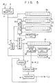
- FIG. 5 An embodiment of the present invention will be described with reference to Fig. 5. This embodiment is arranged to alter the size of small region 2.
- a column selector 20 is provided between M-stage shift registers 13 i , 13:,,..., 13 " and subtractor 18. This selector 20 selects one of shift registers 13 i , 13 2 , 13n in accordance with numerical value n' set in a register 21 and couples it to subtractor 14.
- n' set in a register 21
- a row selector 22 is provided to select one of a plurality of stage outputs of register 15 in accordance with a numerical value m' set in a register 23.
- a row selector 22 is provided to select one of a plurality of stage outputs of register 15 in accordance with a numerical value m' set in a register 23.
- the image processing device of the present invention is not limited to the embodiment described above.
- the shift register as a temporary memory may be replaced by a random access memory (RAM).
- the shift register may be reset directly by a reset signal instead of application of the zero data thereto.
- the alternation of the size of the small region may be performed merely by altering the number of the picture elements in either one of the row and column directions.
- the small region may be tilted with respect to scanning lines and the tilted small region will be obtained by selectively altering the number of stages of the shift registers.
Description
- The present invention relates to an image processing device and, more particularly, to an image processing device arranged to effectively extract the features of small areas of an image.
- When the stains, flaws or defects of a surface of an article is inspected, is often performed such an image processing as picks up the surface of the article by a television camera and measures the density or the number of defects in a region of a predetermined area of the image. In such a conventional image processing method, in order to shorten a processing time, the entire region of the image is fixedly divided into a plurality of regions without overlapping each other, and the image processing is performed for each divided region. The purpose of this image processing is to inspect whether the number of defects or the density in the predetermined area exceeds a predetermined value or threshold value or not. In the case that the image is fixedly divided into a plurality of small regions and the number of defects or the density of each small region is measured, the following problems will arise.
- As shown in Fig. 1, it is assumed that an
image 1 has (MxN) picture elements and is divided intosmall regions 2 each of (mxn) picture elements. It is also assumed that the image processing is performed to inspect the number of defects within the area of each dividedregion 2. For instance, it is also assumed that, a small region which contains more than two defects is rejected on the basis of an inspection criterion. On these assumptions, when defects 3 which are irregularly distributed are inspected, the situations shown in Figs. 2A and 28 might occur. Namely, when theimage 1 is fixedly divided into a plurality ofsmall regions 2 without overlapping each other, there might occur a case where threedefects small region 2 are contained in dividedregion 2 as shown in Fig. 2A, and a case wheredefects region 2 as shown in Fig. 2B. In these cases, thesmall region 2 of Fig. 2A is decided as being rejected, while thesmall region 2 of Fig. 2B is decided as being allowable. In other words, the presence ofdefects - Document US-A-4,162,481 discloses an image processing system in which codes from a scanned source are processed to obtain a continuous updating of a small area sum. This information is used to detect an improperly referenced black/white transmission in an optical character recognition system.
- It is an object of the present invention to provide an image processing device capable of accurately extracting the features containing inspected objects of small regions of an image in which the inspected objects are irregularly distributed, at a high speed.
- In brief, the object of the present invention is achieved by forming a small region of a predetermined number of picture elements in a two- dimensionally scanned image and successively obtaining accumulated output of picture element data of a new small region containing a new picture element each time the new picture element data is read out.
- According to the present invention as claimed, an image to be processed is regarded as having an array of (MxN) picture elements, and the picture elements are sequentially read out by two-dimensional scanning, where N designates the number of scanning lines, and M designates the number of picture elements per one scanning line. A small area is an array of (mxn) picture elements.
- First memory means is provided which receives input picture element data sequentially read out, and has (Mxn) stages to temporarily store (Mxn) picture element data. The data of (Mxn) picture elements thus temporarily stored are read out of the first memory means in the order of application of the (Mxn) picture element data to the memory means. Second memory means of M stages is provided which temporarily stores data which are sequentially input thereto and causes the data thus stored to be sequentially read out in the input sequence. Further, first arithemetic operation circuit means is provided which performs an arithmetic operation of the input picture element data plus the output data of the second memory means minus the output data of the first memory means. The operation result is applied to the second memory means. The data sum of n consecutive picture elements of each row of the picture element array is stored in each stage of the second memory means. The data of each stage is updated every time a new picture element of the corresponding row is read out.
- Further, there are provided third memory means for temporarily storing data and second arithmetic operation circuit means for effecting an arithmetic operation of the output data of the first arithmetic operation circuit plus the output data of the third memory means minus the output data of m(<M)-th stage of the second memory means. The output of the second arithmetic operation circuit means is input to the third memory means. The accumulated sum of the picture element data of a small region consisting of (mxn) picture elements is stored in the third memory means, and is updated every time new picture element data is readout, so that the accumulated data sums of the small regions each having (mxn) picture elements are successively obtained.
- According to the present invention, the accumulated sum of the picture element data of a small area which has (mxn picture elements is sequentially calculated every time a picture element is read out. Thus, the features of small regions can be accurately obtained at a high speed. The picture element data may be a two- valued signal or a multi-valued signal.
- This invention can be more fully understood from the following detailed description when taken in conjunction with the accompanying drawings, in which:
- Fig. 1 is a diagram showing the relationship between an image in which objects to be inspected are irregularly distributed and a small region from which a feature is extracted;
- Figs. 2A and 2B are diagrams for describing the problems in case where small regions are fixed;
- Fig. 3 is a diagram for describing the principle of an image processing according to the present invention;
- Fig. 4 is a block diagram of an image processing device; and
- Fig. 5 is a block diagram of an image processing device according to one embodiment of the present invention.
- Fig. 3 shows the principle of an image processing according to the present invention. In Fig. 3,
reference numeral 1 designates an image which is obtained by two-dimensional scanning of a television camera, and has M picture elements in the scanning line (row) direction and N picture elements in the vertical (column) direction. In general, N is equal to the number of scanning lines.Reference numeral 2 designates a small region which has m picture elements in the row direction and n picture elements in the column direction, and 4 picture elements. Reference numeral 5 depicts the sum of the data of n picture elements in each column ofsmall region 2. - It is assumed here that the accumulated sum Sl-l,j of data of (mxn) picture elements contained in
small region 2 which is defined by positions (i-m, j-n+l) and (i-I, j) and the data sums Sl-m,j' Si-m+1,j to Si-l,j of data of n picture elements of m columns ofsmall region 2 have been obtained. Then, it is also assumed that the data sum of a new small region which is displaced by one row rightwardly is calculated. In this case, data d,,, of a picture element at the position (i, j) is newly input, and the data sum Si,j of n picture elements from position (i, j) to position (i, j-n+I) of i-th row is calcuated. Si,j is obtained by an arithmetic operation of the sum Si,j-l of data of picture elements from position (i, j-I) to (i, j->n) which has already been obtained minus picture element data di,j-n at position (i, j-n) plus new input data di,j In other words,
- The accumulated sum S of (mxn) picture element data in
small region 2 which has i-row at its right end can be obtained as below.
- In this manner, the accumulated sum S¡,j of the picture element data of
small region 2 which is defined by the position (i, j) of a new picture element is sequentially calculated every time new picture element data d,,; is read out by the two-dimensional scanning of image I. Namely, according to the image processing as described above,small regions 2 are successively formed at an interval of one picture element for each row and column over the overall area ofimage 1 according to the two-dimensional scanning ofimage 1, and the accumulated sum of the picture element data in each small region is calculated. Therefore, the problem described with reference to Figs. 2A and 2B can be solved. - A device for executing the above-mentioned calcuation processing of picture element data will be described with reference to Fig. 4.
- Picture element data which are temporarily stored in an image memory are read out serially by two-dimensional scanning. The picture element data di,j thus read out is applied through an
input selector 11 to anadder 12 and afirst shift register 13 which operates as a memory and delay circuit. Theshift register 13 has (Mxn) stages in total, and may be considered as a series connection ofn shift registers image 1, and n is the number of picture elements in the column direction insmall region 2. The data transfer inshift register 13 is effected by clock pulses which are synchronized with the read-out of picture element data from the image memory. Theselector 11 inputs zero data prior to the read-out of data di,j from the image memory, and resets the respective shift registers to zero. - The picture elevent data from
shift register 13 which has been delayed by a period of n lines is applied to asubtractor 14 together with the output data ofadder 12. - The output data of
subtractor 14 is applied to asecon shift register 15 which has M stages and operates as a memory and one-line delay circuit. The output data ofsecond shift register 15 is applied to adder 12 through ashift register 16 which operates as a temporary memory circuit. Theshift register 15 stores the data sum of n picture elements in the respective M rows. Theadder 12 adds new picture element data of each row to the data sum of n picture elements of the corresponding row stored inshift register 15, and the output ofadder 12 represents the data sum of (n+1) picture elements of each row. Thesubtractor 14 subtracts the n-line delayed output data ofshift register 13 from the output data ofadder 12 which represents the sum of (n+1) picture element data of each row so that the data sum of new n picture elements of each row is provided. - The output data of
subtractor 14 is led to anadder 17 to be added to output data of ashift register 18. The output data of m-th stage ofshift register 15 is applied to asubtractor 19 to be subtracted from the output data ofadder 17. The output ofsubtractor 19 represents the accumulated sum Si,j of (mxn) picture element data of a small region which is defined by the position (i, j) of a picture element corresponding to the present input data di,j. Theregister 18 receives the output data ofsubtractor 19 to temporarily store it, and holds the accumulated sum Si-l,j of picture element data in a small region defined by the position (i-I, j) before the input data di,j is applied. - The operation of the image processing device thus arranged will be described. Initially, zero data is applied through
selector 11 to first and second shift registers 13 and 15, thereby resetting the contents of these registers to zero. After shift registers 13 and 15 are reset, picture element data di,j is input throughselector 11. Thus, the data dl,j is sequentially stored infirst shift register 13. At this time, since data which are sequentially read fromshift register 13 all indicate zero, the picture element data of the first line is sequentially stored throughadder 12 andsubtractor 14 inshift register 15. When the picture element data of the next line is input, the output data ofshift register 13 still indicate zero, and the picture element data before one line is read out ofshift register 15, so that the data sums of picture elements of the respective rows on the first and second lines are sequentially applied throughadder 12 to shiftregister 15. In this manner, data sums Sl,n S2,", ... , SM,n of picture element data of n lines in the row direction are stored in the respective stages ofshift register 15. Thereafter, when picture element element data on (n+1)-th line is input, the n-line delayed picture element data are sequentially read out ofshift register 13 to be applied tosubtractor 14. Namely, the data of the n-line preceding picture element of a row is subtracted from the output data ofadder 12 which exhibits the data sum of (n+1) picture elements of the corresponding row. Accordingly, to shiftregister 15 is input the data sum S¡,i which is represented by the following equation as described above.
- On the other hand, the data sum of n picture elements of each row is applied to shift
register 18 throughadder 17 fromsubtractor 14. Accordingly, the data sum of n picture elements are accumulated fro each row. However, since the output data of the m-th stage ofshift register 15 is applied throughsubtractor 19 to register 18, the data sum of m-row preceding n picture elements is subtracted every time the data sum of n picture elements of a new row is output fromsubtractor 17. Namely, inregister 18 the data of (mxn) picture elements formingsmall region 2 are accumulated, and the accumulated sum is updated every time new picture element data is input, with the resultthatthe accumulated sum of (mxn) picture element data is sequentially obtained every small regions displaced by one picture element. - In the arrangement described above, the picture element data may be a binary signal or multi-valued signal. The arrangement described above is suitable for the image processing at the image portion except the periphery of
image 1. In other words it is preferred that, the image portion to be processed by not set to the entire region ofimage 1, but to a portion slighly smaller than the entire region ofimage 1. - An embodiment of the present invention will be described with reference to Fig. 5. This embodiment is arranged to alter the size of
small region 2. In Fig. 5 the same parts as those in Fig. 4 are designated by the same reference numerals and the description thereof will be omitted. Acolumn selector 20 is provided between M-stage shift registers 13i, 13:,,..., 13" andsubtractor 18. Thisselector 20 selects one ofshift registers register 21 and couples it tosubtractor 14. Thus, the number n of the picture elements ofsmall resgion 2 in the column direction can be selectively set. Further, arow selector 22 is provided to select one of a plurality of stage outputs ofregister 15 in accordance with a numerical value m' set in aregister 23. Thus, the number m of the picture elements in row direction ofsmall region 2 can be selectively set in accordance with the numerical value set inregister 23. - The image processing device of the present invention is not limited to the embodiment described above. The shift register as a temporary memory may be replaced by a random access memory (RAM). The shift register may be reset directly by a reset signal instead of application of the zero data thereto. The alternation of the size of the small region may be performed merely by altering the number of the picture elements in either one of the row and column directions. Moreover, the small region may be tilted with respect to scanning lines and the tilted small region will be obtained by selectively altering the number of stages of the shift registers.
Claims (6)
Applications Claiming Priority (4)
| Application Number | Priority Date | Filing Date | Title |
|---|---|---|---|
| JP57082669A JPS58200369A (en) | 1982-05-17 | 1982-05-17 | Picture processor |
| JP57082671A JPS58200371A (en) | 1982-05-17 | 1982-05-17 | Picture processor |
| JP82669/82 | 1982-05-17 | ||
| JP82671/82 | 1982-05-17 |
Publications (3)
| Publication Number | Publication Date |
|---|---|
| EP0094824A2 EP0094824A2 (en) | 1983-11-23 |
| EP0094824A3 EP0094824A3 (en) | 1986-07-16 |
| EP0094824B1 true EP0094824B1 (en) | 1988-12-07 |
Family
ID=26423688
Family Applications (1)
| Application Number | Title | Priority Date | Filing Date |
|---|---|---|---|
| EP83302764A Expired EP0094824B1 (en) | 1982-05-17 | 1983-05-16 | Image processing device for continuously extracting features of small regions of an image |
Country Status (3)
| Country | Link |
|---|---|
| US (1) | US4542527A (en) |
| EP (1) | EP0094824B1 (en) |
| DE (1) | DE3378663D1 (en) |
Cited By (1)
| Publication number | Priority date | Publication date | Assignee | Title |
|---|---|---|---|---|
| US7416136B2 (en) | 2004-03-04 | 2008-08-26 | Parsytec Computer Gmbh | Method for preprocessing surface data, method for quality assessment and for quality management of strip material and apparatus for controlling the processing of strip material |
Families Citing this family (11)
| Publication number | Priority date | Publication date | Assignee | Title |
|---|---|---|---|---|
| US4613948A (en) * | 1984-06-01 | 1986-09-23 | Bell Communications Research, Inc. | Conditional quantization grey level and color image coding apparatus |
| DE3433219A1 (en) * | 1984-09-10 | 1986-03-20 | Will Wetzlar Gmbh, 6330 Wetzlar | Computing device operating electronically |
| US5274717A (en) * | 1985-02-01 | 1993-12-28 | Hitachi, Ltd. | Parallel image processor for performing local neighboring image processing |
| US4881196A (en) * | 1985-02-19 | 1989-11-14 | Mitsubishi Denki Kabushiki Kaisha | Data transmission line branching system |
| FR2583184B1 (en) * | 1985-06-10 | 1989-06-02 | Commissariat Energie Atomique | PROCESS FOR PROCESSING DIGITAL SIGNALS REPRESENTATIVE OF AN ORIGINAL IMAGE |
| US4700400A (en) * | 1985-10-10 | 1987-10-13 | The Palantir Corporation | Feature extraction technique for use in a pattern recognition system |
| US4972502A (en) * | 1987-02-17 | 1990-11-20 | Sharp Kabushiki Kaisha | Image signal binary encoder |
| GB2262339B (en) * | 1991-12-13 | 1995-09-06 | Honda Motor Co Ltd | Method of inspecting the surface of a workpiece |
| US5566244A (en) * | 1993-11-22 | 1996-10-15 | Honda Giken Kogyo Kabushiki Kaisha | Method of inspecting a workpiece surface including a picturing system with a shortened focal plane |
| US5663742A (en) * | 1995-08-21 | 1997-09-02 | Micron Display Technology, Inc. | Compressed field emission display |
| US5854615A (en) * | 1996-10-03 | 1998-12-29 | Micron Display Technology, Inc. | Matrix addressable display with delay locked loop controller |
Family Cites Families (6)
| Publication number | Priority date | Publication date | Assignee | Title |
|---|---|---|---|---|
| US3729619A (en) * | 1971-03-04 | 1973-04-24 | Steel Corp | Apparatus for surface inspection of moving material with defect type recognition |
| US4162481A (en) * | 1976-12-22 | 1979-07-24 | Recognition Equipment Incorporated | Adaptive correlator for video processing |
| US4173441A (en) * | 1977-03-28 | 1979-11-06 | E. I. Du Pont De Nemours And Company | Web inspection system and method therefor |
| IL63781A (en) * | 1980-09-19 | 1985-03-31 | Trw Inc | System for defect analysis in manufactured parts such as turbine blades |
| US4408343A (en) * | 1981-02-27 | 1983-10-04 | Burroughs Corporation | Image enhancement for optical character readers |
| US4398256A (en) * | 1981-03-16 | 1983-08-09 | Hughes Aircraft Company | Image processing architecture |
-
1983
- 1983-05-13 US US06/494,254 patent/US4542527A/en not_active Expired - Fee Related
- 1983-05-16 EP EP83302764A patent/EP0094824B1/en not_active Expired
- 1983-05-16 DE DE8383302764T patent/DE3378663D1/en not_active Expired
Cited By (2)
| Publication number | Priority date | Publication date | Assignee | Title |
|---|---|---|---|---|
| US7416136B2 (en) | 2004-03-04 | 2008-08-26 | Parsytec Computer Gmbh | Method for preprocessing surface data, method for quality assessment and for quality management of strip material and apparatus for controlling the processing of strip material |
| EP1737587B1 (en) | 2004-03-04 | 2016-06-08 | Parsytec Computer GmbH | Method for preparing surface data, method and device for evaluating and managing a strip material quality |
Also Published As
| Publication number | Publication date |
|---|---|
| DE3378663D1 (en) | 1989-01-12 |
| EP0094824A2 (en) | 1983-11-23 |
| US4542527A (en) | 1985-09-17 |
| EP0094824A3 (en) | 1986-07-16 |
Similar Documents
| Publication | Publication Date | Title |
|---|---|---|
| US5440648A (en) | High speed defect detection apparatus having defect detection circuits mounted in the camera housing | |
| EP0094824B1 (en) | Image processing device for continuously extracting features of small regions of an image | |
| US4782399A (en) | Image processing apparatus with high- and low-resolution image sensors and an edge detector | |
| EP0195372B1 (en) | Method and apparatus for forming 3x3 pixel arrays and for performing programmable pattern contingent modifications of those arrays | |
| GB2217145A (en) | Color scanning system | |
| JPH05274359A (en) | Method and device for "consensus synchronous type" data sampling | |
| US4850029A (en) | Adaptive threshold circuit for image processing | |
| EP0371055A1 (en) | Apparatus for enhancing and thresholding scanned microfilm images and methods for use therein. | |
| EP0227406A2 (en) | Image signal processor | |
| US4885787A (en) | High-speed digital image processing apparatus | |
| US5315409A (en) | Method of and apparatus for obtaining binary image | |
| GB2193019A (en) | Data storage | |
| EP0952442A2 (en) | Visual inspection apparatus and method | |
| EP0538042A2 (en) | Apparatus for judging a hand movement of an image | |
| US5046120A (en) | Method of and apparatus for increasing the processing speed in the scanning inspection of circuit boards and other objects | |
| JP3152203B2 (en) | Appearance inspection device | |
| EP0375352B1 (en) | Method of searching a matrix of binary data | |
| US5245424A (en) | Defect detection method | |
| US4242734A (en) | Image corner detector using Haar coefficients | |
| US5299030A (en) | Image data processing method and apparatus with mixture of simple binarization and psuedo intermediate tone | |
| US5034825A (en) | High quality image scanner | |
| EP0455898A1 (en) | Image scanning inspection system | |
| JPH0332723B2 (en) | ||
| US20030138167A1 (en) | Method and a system for stitching images produced by two or more sensors in a graphical scanner | |
| IL100140A (en) | Image storage device and image processing device comprising it |
Legal Events
| Date | Code | Title | Description |
|---|---|---|---|
| PUAI | Public reference made under article 153(3) epc to a published international application that has entered the european phase |
Free format text: ORIGINAL CODE: 0009012 |
|
| 17P | Request for examination filed |
Effective date: 19830527 |
|
| AK | Designated contracting states |
Designated state(s): DE FR GB NL |
|
| RAP1 | Party data changed (applicant data changed or rights of an application transferred) |
Owner name: KABUSHIKI KAISHA TOSHIBA |
|
| PUAL | Search report despatched |
Free format text: ORIGINAL CODE: 0009013 |
|
| AK | Designated contracting states |
Kind code of ref document: A3 Designated state(s): DE FR GB NL |
|
| 17Q | First examination report despatched |
Effective date: 19870630 |
|
| GRAA | (expected) grant |
Free format text: ORIGINAL CODE: 0009210 |
|
| AK | Designated contracting states |
Kind code of ref document: B1 Designated state(s): DE FR GB NL |
|
| REF | Corresponds to: |
Ref document number: 3378663 Country of ref document: DE Date of ref document: 19890112 |
|
| ET | Fr: translation filed | ||
| PLBE | No opposition filed within time limit |
Free format text: ORIGINAL CODE: 0009261 |
|
| STAA | Information on the status of an ep patent application or granted ep patent |
Free format text: STATUS: NO OPPOSITION FILED WITHIN TIME LIMIT |
|
| 26N | No opposition filed | ||
| PGFP | Annual fee paid to national office [announced via postgrant information from national office to epo] |
Ref country code: GB Payment date: 19960507 Year of fee payment: 14 |
|
| PGFP | Annual fee paid to national office [announced via postgrant information from national office to epo] |
Ref country code: FR Payment date: 19960510 Year of fee payment: 14 |
|
| PGFP | Annual fee paid to national office [announced via postgrant information from national office to epo] |
Ref country code: DE Payment date: 19960513 Year of fee payment: 14 |
|
| PGFP | Annual fee paid to national office [announced via postgrant information from national office to epo] |
Ref country code: NL Payment date: 19960529 Year of fee payment: 14 |
|
| PG25 | Lapsed in a contracting state [announced via postgrant information from national office to epo] |
Ref country code: GB Effective date: 19970516 |
|
| PG25 | Lapsed in a contracting state [announced via postgrant information from national office to epo] |
Ref country code: NL Effective date: 19971201 |
|
| GBPC | Gb: european patent ceased through non-payment of renewal fee |
Effective date: 19970516 |
|
| PG25 | Lapsed in a contracting state [announced via postgrant information from national office to epo] |
Ref country code: FR Free format text: LAPSE BECAUSE OF NON-PAYMENT OF DUE FEES Effective date: 19980130 |
|
| NLV4 | Nl: lapsed or anulled due to non-payment of the annual fee |
Effective date: 19971201 |
|
| PG25 | Lapsed in a contracting state [announced via postgrant information from national office to epo] |
Ref country code: DE Free format text: LAPSE BECAUSE OF NON-PAYMENT OF DUE FEES Effective date: 19980203 |
|
| REG | Reference to a national code |
Ref country code: FR Ref legal event code: ST |