EP0458421B1 - Dispositif de lecture/écriture pour cartes à mémoire électronique protégé contre le vandalisme - Google Patents
Dispositif de lecture/écriture pour cartes à mémoire électronique protégé contre le vandalisme Download PDFInfo
- Publication number
- EP0458421B1 EP0458421B1 EP91201606A EP91201606A EP0458421B1 EP 0458421 B1 EP0458421 B1 EP 0458421B1 EP 91201606 A EP91201606 A EP 91201606A EP 91201606 A EP91201606 A EP 91201606A EP 0458421 B1 EP0458421 B1 EP 0458421B1
- Authority
- EP
- European Patent Office
- Prior art keywords
- card
- read
- partition
- card body
- housing
- Prior art date
- Legal status (The legal status is an assumption and is not a legal conclusion. Google has not performed a legal analysis and makes no representation as to the accuracy of the status listed.)
- Expired - Lifetime
Links
Images

Classifications
-
- G—PHYSICS
- G06—COMPUTING OR CALCULATING; COUNTING
- G06K—GRAPHICAL DATA READING; PRESENTATION OF DATA; RECORD CARRIERS; HANDLING RECORD CARRIERS
- G06K7/00—Methods or arrangements for sensing record carriers, e.g. for reading patterns
- G06K7/0013—Methods or arrangements for sensing record carriers, e.g. for reading patterns by galvanic contacts, e.g. card connectors for ISO-7816 compliant smart cards or memory cards, e.g. SD card readers
- G06K7/0086—Methods or arrangements for sensing record carriers, e.g. for reading patterns by galvanic contacts, e.g. card connectors for ISO-7816 compliant smart cards or memory cards, e.g. SD card readers the connector comprising a circuit for steering the operations of the card connector
- G06K7/0091—Methods or arrangements for sensing record carriers, e.g. for reading patterns by galvanic contacts, e.g. card connectors for ISO-7816 compliant smart cards or memory cards, e.g. SD card readers the connector comprising a circuit for steering the operations of the card connector the circuit comprising an arrangement for avoiding intrusions and unwanted access to data inside of the connector
-
- G—PHYSICS
- G06—COMPUTING OR CALCULATING; COUNTING
- G06K—GRAPHICAL DATA READING; PRESENTATION OF DATA; RECORD CARRIERS; HANDLING RECORD CARRIERS
- G06K13/00—Conveying record carriers from one station to another, e.g. from stack to punching mechanism
- G06K13/02—Conveying record carriers from one station to another, e.g. from stack to punching mechanism the record carrier having longitudinal dimension comparable with transverse dimension, e.g. punched card
- G06K13/08—Feeding or discharging cards
- G06K13/0868—Feeding or discharging cards using an arrangement for keeping the feeding or insertion slot of the card station clean of dirt, or to avoid feeding of foreign or unwanted objects into the slot
- G06K13/0893—Feeding or discharging cards using an arrangement for keeping the feeding or insertion slot of the card station clean of dirt, or to avoid feeding of foreign or unwanted objects into the slot the arrangement comprising means for cleaning the card upon insertion
-
- G—PHYSICS
- G06—COMPUTING OR CALCULATING; COUNTING
- G06K—GRAPHICAL DATA READING; PRESENTATION OF DATA; RECORD CARRIERS; HANDLING RECORD CARRIERS
- G06K7/00—Methods or arrangements for sensing record carriers, e.g. for reading patterns
- G06K7/0013—Methods or arrangements for sensing record carriers, e.g. for reading patterns by galvanic contacts, e.g. card connectors for ISO-7816 compliant smart cards or memory cards, e.g. SD card readers
- G06K7/0021—Methods or arrangements for sensing record carriers, e.g. for reading patterns by galvanic contacts, e.g. card connectors for ISO-7816 compliant smart cards or memory cards, e.g. SD card readers for reading/sensing record carriers having surface contacts
-
- G—PHYSICS
- G06—COMPUTING OR CALCULATING; COUNTING
- G06K—GRAPHICAL DATA READING; PRESENTATION OF DATA; RECORD CARRIERS; HANDLING RECORD CARRIERS
- G06K7/00—Methods or arrangements for sensing record carriers, e.g. for reading patterns
- G06K7/0013—Methods or arrangements for sensing record carriers, e.g. for reading patterns by galvanic contacts, e.g. card connectors for ISO-7816 compliant smart cards or memory cards, e.g. SD card readers
- G06K7/0021—Methods or arrangements for sensing record carriers, e.g. for reading patterns by galvanic contacts, e.g. card connectors for ISO-7816 compliant smart cards or memory cards, e.g. SD card readers for reading/sensing record carriers having surface contacts
- G06K7/003—Methods or arrangements for sensing record carriers, e.g. for reading patterns by galvanic contacts, e.g. card connectors for ISO-7816 compliant smart cards or memory cards, e.g. SD card readers for reading/sensing record carriers having surface contacts means for pressing the connector contacts in the direction of the card contacts to assure trustworthy electrical connection between card and connector
Definitions
- the present invention relates to a device for read / write for protected electronic memory cards against vandalism.
- Such a card basically consists of a generally rectangular card body in which an electronic module is installed.
- the electronic module includes an integrated circuit comprising at least one circuit memory and external electrical contact ranges which are connected to the terminals of the integrated circuit.
- Processing machine includes circuits of processing to exploit the information contained in the card memory and to change these information and a read / write device that provides a temporary electrical connection between card contact areas and circuits machine processing. The establishment of this connection is used to power the integrated circuit of the card, to transmit the instructions for writing / reading the card memory, apply write voltage and a clock signal etc ...
- a read / write device usually includes a case which has on its front face a slot card introduction and which internally defines a guideway used to position the card in such a way so that when it is in the position of processing, i.e. in the depressed position, the ranges contact card are in electrical contact with a connector which is mounted in the guideway.
- contact pads are arranged near a corner of the body of the card. The connector of the device read / write is therefore offset from the plane median of the read / write device.
- Document DE 36 02 668 describes a card reader in which the card is placed on a mobile carriage in translation. When the carriage reaches the position of reading, it lifts slightly to apply the contacts of the card to the head reading, which causes a slight curvature of the body of the card.
- An object of the invention is to provide a read / write device for credit cards. electronic memory to prevent these acts of vandalism or less to make them more difficult.
- the invention relates to a read / write device according to claim 1.
- card reader will be called the reading and / or writing for electronic memory cards.
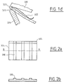
- Figures la to ld show an embodiment of the card reader. he includes a housing 302 formed by a partition upper 304, two side partitions 306 and 308 and a portion of the lower partition 310. The two lateral partitions 306 and 308 are separated by a distance substantially equal to the width of the card body.
- the upper face 310a of the lower partition 310 and the front part 312 of the upper partition 304 define between the side partitions an insertion slot 314 for the card. Slot 314 allows the card to be inserted into the cavity 316 defined by the housing, the cavity 316 not comprising no background.
- the cavity 316 comprises a substantially flat inclined partition 324 whose edges are integral with the side partitions 306 and 308 of the housing.
- the partition 324 has an inclination greater than that of the head of reading 308.
- the partition 316 ends with a bevel 325 which has a lower inclination of the main face of partition 326, as shown in Figure 1d.
- the curvature of the card body is controlled by a span plane 326 forming a step 327 in the cavity 316 to from the upper wall 304. In this position the contact pads 346 on the card are connected to the conductive blades 322 of the read head.
- bevel 325 allows the user to "feel” that the card will come to a stop on the stop mechanical 323.
- the face of the partition 324 on which the front edge rubs 340a of the map is still noticeably flat but it has ribs 330 arranged in the direction of introduction of the card and which form a very slight projection from the main face of the partition 324.
- Partition 324 occupies the entire width of the cavity 316 it it is sufficient that the partition has sufficient width to guide the end of the card body and give it the bending required.
- Partition 324 could also consist of several parallel partition elements separated by intervals, the partition elements being all arranged in one plane.
- the curvature taken by the front portion of the card body performs several functions. On the one hand it stiffens the portion of the card body in contact with the head of reading which ensures good electrical contact between the card and the read head although the card does not rest on no partition in the portion bearing the ranges of contacts.
- the map when deformed comes to be pressed on the connector contacts, the friction stroke being very small but sufficient to ensure a car cleaning of the contacts due to the steep inclination of the partition 324 which is of the order of 36 degrees. So does even for the embodiments of FIGS. 5 and 6.
- this curvature ensures immobilization the card during the processing phase of this one.
- the card reader effectively avoids acts of vandalism. Indeed, the cavity 316 not comprising no substance, objects introduced maliciously into the reader fall.
- the read head 318 is arranged behind the upper part 326 in the offset 327, so it is not possible, or for the less very difficult to insert an object through the slot 314 rigid to try to damage the conductive blades of the read head 318.
Landscapes
- Engineering & Computer Science (AREA)
- Physics & Mathematics (AREA)
- General Physics & Mathematics (AREA)
- Theoretical Computer Science (AREA)
- Artificial Intelligence (AREA)
- Computer Vision & Pattern Recognition (AREA)
- Coupling Device And Connection With Printed Circuit (AREA)
- Conveying Record Carriers (AREA)
- Credit Cards Or The Like (AREA)
- Packaging Of Annular Or Rod-Shaped Articles, Wearing Apparel, Cassettes, Or The Like (AREA)
Description
- la figure la est une vue en coupe longitudinale, selon le plan A-A de la figure 1b, d'un mode de réalisation du dispositif de lecture/écriture ;
- la figure 1b est une vue de face du dispositif de lecture/écriture de la figure 1a ;
- la figure 1c est une vue en coupe verticale selon la ligne C-C de la figure la d'un mode de réalisation du dispositif de lecture/écriture ;
- la figure ld est une vue de détail de la figure 1a ; et
- les figures 2a et 2b montrent une variante de réalisation du lecteur des figures la à ld respectivement en vue de face et en coupe selon la ligne B-B de la figure 2a.
Claims (4)
- Dispositif de lecture/écriture pour des cartes à mémoire électronique comprenant un corps de carte (340) et des plages de contact électrique (346) disposées dans une des faces principales dudit corps de carte, ledit dispositif comprenant un boítier (302) muni d'une ouverture frontale (314) pour permettre l'introduction de ladite carte dans ledit boítier ; une tête de lecture/écriture (318) comprenant des éléments de connexion (322) disposée à l'intérieur dudit boítier ; des moyens de guidage de ladite carte pour guider celle-ci entre ladite ouverture frontale et une position de traitement dans laquelle lesdites plages de contact sont aptes à entrer en contact avec lesdits éléments de connexion de ladite tête de lecture/écriture, des moyens de maintien de la portion dudit corps de carte comportant lesdites plages de contact lorsque ladite carte est en position de traitement, lesdits moyens de maintien comprenant des moyens (324, 310) pour supporter les extrémités de la face inférieure dudit corps de carte lorsque ladite carte est en position de lecture et des moyens fixes (326) coopérant avec lesdits moyens de supportage pour provoquer une courbure de la portion du corps de carte portant lesdites plages de contact électrique (346) par quoi lesdites plages de contact électrique (346) sont appliquées contre les éléments de connexion (322) de ladite tête de lecture/écriture lorsque ladite carte est en position de lecture, caractérisé en ce que lesdits moyens de supportage sont des moyens fixes (324, 310), ledit boítier (302) étant totalement dépourvu de fond entre lesdits moyens de supportage.
- Dispositif de lecture/écriture selon la revendication 1, caractérisé en ce que lesdits moyens pour provoquer la courbure du corps de carte comprennent une cloison (324) sensiblement plane inclinée par rapport à la direction d'introduction de la carte et disposée sensiblement en regard de la tête de lecture/écriture (318), la distance selon la direction d'introduction de la carte entre ladite ouverture frontale (314) et ladite cloison (324) étant inférieure à la dimension de ladite carte (340) selon ladite direction.
- Dispositif de lecture/écriture selon l'une quelconque des revendications 1 et 2, caractérisé en ce que ladite ouverture frontale (314) a la forme d'une fente dont la hauteur est sensiblement égale à l'épaisseur du corps de carte, et en ce que ledit boítier (302) définit une cavité interne (316) dépourvue de fond dans laquelle est disposée ladite cloison (324) inclinée ainsi qu'un autre élément de cloison (326) sur lequel s'appuie la face du corps de carte portant les plages de contact lorsque ledit corps de carte (340) subit ladite courbure.
- Dispositif selon l'une quelconque des revendications 2 et 3, caractérisé en ce que ladite cloison inclinée (324) comporte au moins une nervure (330) disposée selon la direction d'introduction de ladite carte.
Applications Claiming Priority (5)
| Application Number | Priority Date | Filing Date | Title |
|---|---|---|---|
| FR8704992A FR2613854B1 (fr) | 1987-04-09 | 1987-04-09 | Dispositif de lecture/ecriture pour cartes a memoire electronique protege contre le vandalisme |
| FR8704992 | 1987-04-09 | ||
| FR8714601 | 1987-10-22 | ||
| FR8714601A FR2622321B1 (fr) | 1987-10-22 | 1987-10-22 | Dispositif de lecture/ecriture pour cartes a memoire electronique protege contre le vandalisme |
| EP88400743A EP0287417B1 (fr) | 1987-04-09 | 1988-03-28 | Dispositif de lecture/écriture pour cartes à mémoire électronique protégé contre le vandalisme |
Related Parent Applications (2)
| Application Number | Title | Priority Date | Filing Date |
|---|---|---|---|
| EP88400743A Division EP0287417B1 (fr) | 1987-04-09 | 1988-03-28 | Dispositif de lecture/écriture pour cartes à mémoire électronique protégé contre le vandalisme |
| EP88400743.6 Division | 1988-03-28 |
Publications (3)
| Publication Number | Publication Date |
|---|---|
| EP0458421A2 EP0458421A2 (fr) | 1991-11-27 |
| EP0458421A3 EP0458421A3 (en) | 1993-07-07 |
| EP0458421B1 true EP0458421B1 (fr) | 1999-10-06 |
Family
ID=26225910
Family Applications (2)
| Application Number | Title | Priority Date | Filing Date |
|---|---|---|---|
| EP91201606A Expired - Lifetime EP0458421B1 (fr) | 1987-04-09 | 1988-03-28 | Dispositif de lecture/écriture pour cartes à mémoire électronique protégé contre le vandalisme |
| EP88400743A Expired - Lifetime EP0287417B1 (fr) | 1987-04-09 | 1988-03-28 | Dispositif de lecture/écriture pour cartes à mémoire électronique protégé contre le vandalisme |
Family Applications After (1)
| Application Number | Title | Priority Date | Filing Date |
|---|---|---|---|
| EP88400743A Expired - Lifetime EP0287417B1 (fr) | 1987-04-09 | 1988-03-28 | Dispositif de lecture/écriture pour cartes à mémoire électronique protégé contre le vandalisme |
Country Status (5)
| Country | Link |
|---|---|
| US (1) | US4873425A (fr) |
| EP (2) | EP0458421B1 (fr) |
| JP (1) | JPS63271677A (fr) |
| DE (2) | DE3869178D1 (fr) |
| ES (1) | ES2030877T3 (fr) |
Families Citing this family (14)
| Publication number | Priority date | Publication date | Assignee | Title |
|---|---|---|---|---|
| FR2658338A1 (fr) * | 1990-02-09 | 1991-08-16 | Landis Gyr | Connecteur electrique pour carte portant un circuit. |
| FR2668096B1 (fr) * | 1990-10-19 | 1993-01-22 | Schlumberger Ind Sa | Procede de fabrication de carte a memoire apte a recevoir une image photographique et carte ainsi obtenue. |
| FR2675929B1 (fr) * | 1991-04-26 | 1993-07-02 | Cit Alcatel | Lecteur de carte a puce. |
| DE69222849T2 (de) * | 1992-08-21 | 1998-03-26 | Alsthom Cge Alcatel | Karteneinführungsvorrichtung |
| JP2660655B2 (ja) * | 1993-12-16 | 1997-10-08 | アンリツ株式会社 | Icカード処理装置 |
| US5563397A (en) * | 1993-12-16 | 1996-10-08 | Anritsu Corporation | Cards receiving mechanism having function for certainly receiving qualified cards and blocking unqualified cards and foreign articles |
| US5850079A (en) * | 1995-02-22 | 1998-12-15 | Sankyo Seiki Mfg.Co., Ltd. | Card reader with a theft counter measure |
| JPH0950492A (ja) * | 1995-08-09 | 1997-02-18 | Olympus Optical Co Ltd | 情報処理装置 |
| DE29607253U1 (de) * | 1996-04-22 | 1996-07-04 | Stocko Metallwarenfabriken Henkels & Sohn GmbH & Co, 42327 Wuppertal | Kombichipkartenleser |
| JPH1055415A (ja) * | 1996-08-08 | 1998-02-24 | Anritsu Corp | カード処理装置 |
| JP3395950B2 (ja) | 1997-08-08 | 2003-04-14 | タイコエレクトロニクスアンプ株式会社 | カード用コネクタ |
| DE19743936C2 (de) | 1997-10-04 | 1999-11-04 | Hopt & Schuler Ddm | Kartenleser |
| DE29721637U1 (de) * | 1997-11-25 | 1998-02-05 | Thomas & Betts Corp | Gerät zum Lesen von Chipkarten |
| JP4829643B2 (ja) | 2006-03-02 | 2011-12-07 | 日立オムロンターミナルソリューションズ株式会社 | カードリーダ |
Family Cites Families (10)
| Publication number | Priority date | Publication date | Assignee | Title |
|---|---|---|---|---|
| FR2415378A1 (fr) * | 1978-01-24 | 1979-08-17 | Moreno Roland | Procede et dispositif pour connecter electriquement un objet amovible notamment une carte electronique portative |
| FR2445560B1 (fr) * | 1978-12-27 | 1985-09-13 | Cii Honeywell Bull | Connecteur pour objets portatifs, notamment des cartes de credit |
| FR2477303B1 (fr) * | 1980-02-28 | 1986-09-26 | Dassault Electronique | Dispositif de lecture de cartes electroniques |
| JPS6031671A (ja) * | 1983-08-01 | 1985-02-18 | Oki Electric Ind Co Ltd | Idカ−ド読取り,書込み装置 |
| DE3402632A1 (de) * | 1984-01-26 | 1985-08-01 | Siemens AG, 1000 Berlin und 8000 München | Verfahren und vorrichtung zur auswertung einer wertkarte in einem kartenleser |
| US4724310A (en) * | 1984-07-02 | 1988-02-09 | Tokyo Tatsuno Co., Ltd. | Device for inserting and holding an IC card as an external memory during reading and writing operations |
| DE3445185A1 (de) * | 1984-12-11 | 1986-06-12 | Nixdorf Computer Ag, 4790 Paderborn | Aufnahmeeinheit fuer eine einen elektronischen schaltkreis enthaltende datenkarte |
| FR2575867B1 (fr) * | 1985-01-09 | 1987-03-06 | Ckd Electronique | Connecteur pour objets portatifs incluant un circuit electrique ou electronique, tels qu'une carte electronique |
| FR2587132B1 (fr) * | 1985-09-12 | 1987-11-20 | Bull Transac | Procede de confiscation d'une carte pour un lecteur mixte et lecteur mixte |
| DE3645268C2 (de) * | 1986-01-29 | 1996-08-14 | Amphenol Corp | Kartenaufnehmner für ein Lesegerät für eine Chip-Karte |
-
1988
- 1988-03-28 DE DE8888400743T patent/DE3869178D1/de not_active Expired - Fee Related
- 1988-03-28 EP EP91201606A patent/EP0458421B1/fr not_active Expired - Lifetime
- 1988-03-28 ES ES198888400743T patent/ES2030877T3/es not_active Expired - Lifetime
- 1988-03-28 EP EP88400743A patent/EP0287417B1/fr not_active Expired - Lifetime
- 1988-03-28 DE DE3856365T patent/DE3856365T2/de not_active Expired - Fee Related
- 1988-04-06 US US07/178,164 patent/US4873425A/en not_active Expired - Fee Related
- 1988-04-08 JP JP63087081A patent/JPS63271677A/ja active Pending
Also Published As
| Publication number | Publication date |
|---|---|
| DE3856365T2 (de) | 2000-03-02 |
| US4873425A (en) | 1989-10-10 |
| ES2030877T3 (es) | 1992-11-16 |
| EP0287417A1 (fr) | 1988-10-19 |
| EP0458421A3 (en) | 1993-07-07 |
| EP0458421A2 (fr) | 1991-11-27 |
| DE3856365D1 (de) | 1999-11-11 |
| EP0287417B1 (fr) | 1992-03-18 |
| JPS63271677A (ja) | 1988-11-09 |
| DE3869178D1 (de) | 1992-04-23 |
Similar Documents
| Publication | Publication Date | Title |
|---|---|---|
| EP0458421A2 (fr) | Dispositif de lecture/écriture pour cartes à mémoire électronique protégé contre le vandalisme | |
| EP0515897B1 (fr) | Connecteur pour carte à circuits | |
| EP0860904B1 (fr) | Connecteur pour le raccordement d'une carte à circuit(s) intégré(s) et boítier équipé d'un tel connecteur | |
| EP0576338B1 (fr) | Lecteur de carte à puce | |
| EP0951094B1 (fr) | Dispositif de connexion autodénudant | |
| FR2550014A1 (fr) | Monture de pile electrique, pour piles plates | |
| FR2821988A1 (fr) | Connecteur electrique pour cartes a memoire electronique a grande capacite de stockage | |
| FR2809871A1 (fr) | Connecteur electrique a lames de contact perfectionnees pour le raccordement d'une carte a circuit(s) integre(s) | |
| EP0510599A1 (fr) | Lecteur de carte à puce | |
| EP0333530B2 (fr) | Perfectionnements aux boîtiers connecteurs pour cartes à microcircuits | |
| EP0675456B1 (fr) | Boítier pour lecteur de carte à microcircuit | |
| EP1588459A1 (fr) | Connecteur a fiches munis de bornes de contact a compression | |
| FR2714534A1 (fr) | Bande de contacts et connecteur pour carte la comprenant. | |
| FR2607944A1 (fr) | Dispositif de lecture/ecriture pour cartes a memoire electronique | |
| EP0980561B2 (fr) | Carte amovible a connecteur enfichable, formant lecteur de carte a puce pour micro-ordinateur | |
| EP0822507B1 (fr) | Détecteur de support plat et connecteur comportant un tel détecteur | |
| FR2575867A1 (fr) | Connecteur pour objets portatifs incluant un circuit electrique ou electronique, tels qu'une carte electronique | |
| EP0656597B1 (fr) | Cadre de contact et connecteur pour carte | |
| FR2622321A1 (fr) | Dispositif de lecture/ecriture pour cartes a memoire electronique protege contre le vandalisme | |
| EP0982679A1 (fr) | Connecteur de lecteur de carte sim | |
| EP0643856B1 (fr) | Recepteur de carte permettant l'ejection d'une carte cassee et lecteur de carte l'utilisant | |
| EP0996930A1 (fr) | Support pour un circuit electronique, comprenant des moyens anti-arrachement | |
| EP1131770B1 (fr) | Dispositif de lecture de carte a microcircuit | |
| EP0086714A1 (fr) | Connecteur pour cartes à circuits imprimés | |
| EP1181662B1 (fr) | Procede et dispositif de prise d'un contact electrique sur une carte a puce |
Legal Events
| Date | Code | Title | Description |
|---|---|---|---|
| PUAI | Public reference made under article 153(3) epc to a published international application that has entered the european phase |
Free format text: ORIGINAL CODE: 0009012 |
|
| AC | Divisional application: reference to earlier application |
Ref document number: 287417 Country of ref document: EP |
|
| AK | Designated contracting states |
Kind code of ref document: A2 Designated state(s): BE CH DE ES GB IT LI NL SE |
|
| PUAL | Search report despatched |
Free format text: ORIGINAL CODE: 0009013 |
|
| AK | Designated contracting states |
Kind code of ref document: A3 Designated state(s): BE CH DE ES GB IT LI NL SE |
|
| 17P | Request for examination filed |
Effective date: 19931110 |
|
| 17Q | First examination report despatched |
Effective date: 19941214 |
|
| GRAG | Despatch of communication of intention to grant |
Free format text: ORIGINAL CODE: EPIDOS AGRA |
|
| GRAG | Despatch of communication of intention to grant |
Free format text: ORIGINAL CODE: EPIDOS AGRA |
|
| GRAH | Despatch of communication of intention to grant a patent |
Free format text: ORIGINAL CODE: EPIDOS IGRA |
|
| RAP1 | Party data changed (applicant data changed or rights of an application transferred) |
Owner name: SCHLUMBERGER SYSTEMES |
|
| GRAH | Despatch of communication of intention to grant a patent |
Free format text: ORIGINAL CODE: EPIDOS IGRA |
|
| GRAA | (expected) grant |
Free format text: ORIGINAL CODE: 0009210 |
|
| AC | Divisional application: reference to earlier application |
Ref document number: 287417 Country of ref document: EP |
|
| AK | Designated contracting states |
Kind code of ref document: B1 Designated state(s): BE CH DE ES GB IT LI NL SE |
|
| PG25 | Lapsed in a contracting state [announced via postgrant information from national office to epo] |
Ref country code: SE Free format text: THE PATENT HAS BEEN ANNULLED BY A DECISION OF A NATIONAL AUTHORITY Effective date: 19991006 Ref country code: NL Free format text: LAPSE BECAUSE OF FAILURE TO SUBMIT A TRANSLATION OF THE DESCRIPTION OR TO PAY THE FEE WITHIN THE PRESCRIBED TIME-LIMIT Effective date: 19991006 Ref country code: GB Free format text: LAPSE BECAUSE OF FAILURE TO SUBMIT A TRANSLATION OF THE DESCRIPTION OR TO PAY THE FEE WITHIN THE PRESCRIBED TIME-LIMIT Effective date: 19991006 Ref country code: ES Free format text: THE PATENT HAS BEEN ANNULLED BY A DECISION OF A NATIONAL AUTHORITY Effective date: 19991006 |
|
| REG | Reference to a national code |
Ref country code: CH Ref legal event code: EP |
|
| REF | Corresponds to: |
Ref document number: 3856365 Country of ref document: DE Date of ref document: 19991111 |
|
| ITF | It: translation for a ep patent filed | ||
| NLV1 | Nl: lapsed or annulled due to failure to fulfill the requirements of art. 29p and 29m of the patents act | ||
| PG25 | Lapsed in a contracting state [announced via postgrant information from national office to epo] |
Ref country code: LI Free format text: LAPSE BECAUSE OF NON-PAYMENT OF DUE FEES Effective date: 20000331 Ref country code: CH Free format text: LAPSE BECAUSE OF NON-PAYMENT OF DUE FEES Effective date: 20000331 Ref country code: BE Free format text: LAPSE BECAUSE OF NON-PAYMENT OF DUE FEES Effective date: 20000331 |
|
| GBV | Gb: ep patent (uk) treated as always having been void in accordance with gb section 77(7)/1977 [no translation filed] |
Effective date: 19991006 |
|
| PLBE | No opposition filed within time limit |
Free format text: ORIGINAL CODE: 0009261 |
|
| STAA | Information on the status of an ep patent application or granted ep patent |
Free format text: STATUS: NO OPPOSITION FILED WITHIN TIME LIMIT |
|
| 26N | No opposition filed | ||
| BERE | Be: lapsed |
Owner name: SCHLUMBERGER SYSTEMES Effective date: 20000331 |
|
| REG | Reference to a national code |
Ref country code: CH Ref legal event code: PL |
|
| PGFP | Annual fee paid to national office [announced via postgrant information from national office to epo] |
Ref country code: DE Payment date: 20020404 Year of fee payment: 15 |
|
| PG25 | Lapsed in a contracting state [announced via postgrant information from national office to epo] |
Ref country code: DE Free format text: LAPSE BECAUSE OF NON-PAYMENT OF DUE FEES Effective date: 20031001 |
|
| PG25 | Lapsed in a contracting state [announced via postgrant information from national office to epo] |
Ref country code: IT Free format text: LAPSE BECAUSE OF NON-PAYMENT OF DUE FEES;WARNING: LAPSES OF ITALIAN PATENTS WITH EFFECTIVE DATE BEFORE 2007 MAY HAVE OCCURRED AT ANY TIME BEFORE 2007. THE CORRECT EFFECTIVE DATE MAY BE DIFFERENT FROM THE ONE RECORDED. Effective date: 20050328 |