EP0457160A1 - Cascode mirror video amplifier - Google Patents
Cascode mirror video amplifier Download PDFInfo
- Publication number
- EP0457160A1 EP0457160A1 EP91107408A EP91107408A EP0457160A1 EP 0457160 A1 EP0457160 A1 EP 0457160A1 EP 91107408 A EP91107408 A EP 91107408A EP 91107408 A EP91107408 A EP 91107408A EP 0457160 A1 EP0457160 A1 EP 0457160A1
- Authority
- EP
- European Patent Office
- Prior art keywords
- common
- amplifier
- emitter
- pair
- base
- Prior art date
- Legal status (The legal status is an assumption and is not a legal conclusion. Google has not performed a legal analysis and makes no representation as to the accuracy of the status listed.)
- Granted
Links
- 230000007704 transition Effects 0.000 claims description 6
- 239000000872 buffer Substances 0.000 claims description 3
- 230000002708 enhancing effect Effects 0.000 claims 4
- 238000005070 sampling Methods 0.000 claims 1
- 238000010586 diagram Methods 0.000 description 3
- 238000010276 construction Methods 0.000 description 2
- 230000000694 effects Effects 0.000 description 2
- 238000012986 modification Methods 0.000 description 2
- 230000004048 modification Effects 0.000 description 2
- OAICVXFJPJFONN-UHFFFAOYSA-N Phosphorus Chemical compound [P] OAICVXFJPJFONN-UHFFFAOYSA-N 0.000 description 1
- 230000003321 amplification Effects 0.000 description 1
- 239000011248 coating agent Substances 0.000 description 1
- 238000000576 coating method Methods 0.000 description 1
- 230000003247 decreasing effect Effects 0.000 description 1
- 230000001747 exhibiting effect Effects 0.000 description 1
- 239000003574 free electron Substances 0.000 description 1
- 238000003199 nucleic acid amplification method Methods 0.000 description 1
- 230000000007 visual effect Effects 0.000 description 1
Images
Classifications
-
- H—ELECTRICITY
- H04—ELECTRIC COMMUNICATION TECHNIQUE
- H04N—PICTORIAL COMMUNICATION, e.g. TELEVISION
- H04N9/00—Details of colour television systems
- H04N9/64—Circuits for processing colour signals
- H04N9/648—Video amplifiers
-
- H—ELECTRICITY
- H03—ELECTRONIC CIRCUITRY
- H03F—AMPLIFIERS
- H03F1/00—Details of amplifiers with only discharge tubes, only semiconductor devices or only unspecified devices as amplifying elements
- H03F1/08—Modifications of amplifiers to reduce detrimental influences of internal impedances of amplifying elements
- H03F1/22—Modifications of amplifiers to reduce detrimental influences of internal impedances of amplifying elements by use of cascode coupling, i.e. earthed cathode or emitter stage followed by earthed grid or base stage respectively
-
- H—ELECTRICITY
- H03—ELECTRONIC CIRCUITRY
- H03F—AMPLIFIERS
- H03F3/00—Amplifiers with only discharge tubes or only semiconductor devices as amplifying elements
- H03F3/26—Push-pull amplifiers; Phase-splitters therefor
-
- H—ELECTRICITY
- H03—ELECTRONIC CIRCUITRY
- H03F—AMPLIFIERS
- H03F3/00—Amplifiers with only discharge tubes or only semiconductor devices as amplifying elements
- H03F3/42—Amplifiers with two or more amplifying elements having their DC paths in series with the load, the control electrode of each element being excited by at least part of the input signal, e.g. so-called totem-pole amplifiers
Definitions
- the cathode In operation, the cathode is heated to boil off free electrons.
- the control grid of the gun alternately enables and disables the electron flow as a function of negative potential.
- Various combinations of bias control are effective for operating the triode.
- the electron flow from the cathode can be controlled by means of the video signal while holding the control grid at a constant cut-off potential relative to the accelerator grid.
- the video signal can be applied to the control grid while the cathode potential is maintained constant, or the video signal can be applied to the control grid and cathode with opposite phase.
- Optimum performance of projection CRT guns has been found to occur with the cut-off (i.e. no electron flow) potential between the cathode and control grid to a potential maintained at a predetermined value (e.g. typically 150 volts). This is done by biasing the accelerator grid to a potential (e.g. 400 volts to 1000 volts) at which electron flow is barely stopped when the cathode and control grid potential is set at the aforementioned cut-off potential.
- a potential e.g. 400 volts to 1000 volts
- a cascode mirror high bandwidth video amplifier is provided for driving the cathode and control grid of a CRT electron gun with equal amplitude and opposite phase voltage signals, thereby overcoming the delay variations inherent in the latter mentioned prior art approach.
- a driver transistor is utilized in the form of a voltage controlled current source intermediate a pair of cascode amplifiers such that the current flowing through the load resistors of the amplifiers are common to both, thereby eliminating delay variations between the opposite phase signals.
- a video amplifier for controlling an electron source cathode and a control grid of a cathode ray tube comprising:
- emitter follower output stages 5 and 9 Additional details of construction and operation of emitter follower output stages 5 and 9 are not discussed in detail herein but would be well known to a person skilled in the art.
- the combined voltage output results in a total signal swing amplitude of as high as 140 volts.
- the magnitude of the voltage signal swing depends on the biasing voltages of the common base transistors 1 and 7.
- transistors 1 and 7 are biased at +6 volts and -1 volts via respective DC bias voltage sources 17 and 19.
- the maximum output swing voltage for the successful prototype can be expressed as (85-6-Vcb1) + (85-1-Vbc7), where Vcb1 denotes the collector-base voltage of transistor 1 and Vcb7 denotes the collector-base voltage of transistor 7.
- the maximum signal current is thus (85-6-Vcb1)/R12 for linear operation.
Landscapes
- Engineering & Computer Science (AREA)
- Power Engineering (AREA)
- Multimedia (AREA)
- Signal Processing (AREA)
- Amplifiers (AREA)
- Picture Signal Circuits (AREA)
Abstract
Description
- This invention relates in general to video display systems, and more particularly to a cascode mirror video amplifier for driving the electron source cathode and control grid of a cathode ray tube.
- The electron gun of a cathode ray tube (CRT) consists of two sections - the triode and the lens. The lens focuses the emitted electrons using three typically cylindrical elements aligned end to end on the gun axis with the triode. The triode forms the electron emitting section of the gun and comprises an electron source cathode, control grid and accelerator grid.
- In operation, the cathode is heated to boil off free electrons. The control grid of the gun alternately enables and disables the electron flow as a function of negative potential. Various combinations of bias control are effective for operating the triode. For example, the electron flow from the cathode can be controlled by means of the video signal while holding the control grid at a constant cut-off potential relative to the accelerator grid. Alternatively, the video signal can be applied to the control grid while the cathode potential is maintained constant, or the video signal can be applied to the control grid and cathode with opposite phase.
- Optimum performance of projection CRT guns has been found to occur with the cut-off (i.e. no electron flow) potential between the cathode and control grid to a potential maintained at a predetermined value (e.g. typically 150 volts). This is done by biasing the accelerator grid to a potential (e.g. 400 volts to 1000 volts) at which electron flow is barely stopped when the cathode and control grid potential is set at the aforementioned cut-off potential.
- Thus, when the potential between the control grid and cathode is decreased from the cut-off value, electrons are caused to flow from the cathode to the phosphor coating on the viewing surface of the CRT, resulting in generation of a visual image. The maximum allowable current flow occurs when the potential between the control grid and cathode is zero volts.
- According to the prior art, wide dynamic range video amplifiers have been utilized to control the potential between the cathode and control grid of a CRT electron gun. One prior art approach utilizes cascode video amplifiers incorporating high voltage transistors. However, it has been found that such high voltage video transistors are characterized by limited frequency response and therefore incapable of providing the wide dynamic range and high bandwidth required for high resolution projections systems.
- According to another prior art approach, a pair of smaller cascode amplifiers have been utilized for driving the cathode and control grid with opposite phase signals. However, this approach results in phase problems due to the delay variations between response times of the two cascode amplifiers.
- According to the present invention, a cascode mirror high bandwidth video amplifier is provided for driving the cathode and control grid of a CRT electron gun with equal amplitude and opposite phase voltage signals, thereby overcoming the delay variations inherent in the latter mentioned prior art approach. More particularly, a driver transistor is utilized in the form of a voltage controlled current source intermediate a pair of cascode amplifiers such that the current flowing through the load resistors of the amplifiers are common to both, thereby eliminating delay variations between the opposite phase signals.
- In accordance with an aspect of the present invention, there is provided a circuit for generating equal-amplitude and opposite phase signals, comprising a pair of cascaded amplifiers connected via respective equal valued resistances to a pair of opposite polarity power sources, and a voltage controlled current source common to each said pair of amplifiers for receiving an input signal and in response generating a common current signal within each said pair of amplifiers such that equal amplitude and opposite phase voltage signals are generated across said respective resistances.
- In accordance with another aspect of the present invention there is provided a video amplifier for controlling an electron source cathode and a control grid of a cathode ray tube, comprising:
- a) a first cascode stage connected to a first DC power source through a first pull-up resistor;
- b) a second cascode stage connected to a second DC power source through a second pull-up resistor;
- c) a voltage controlled current source common to each said first and second stages for receiving an input signal and in response generating a common current signal within each said first and second stages such that respective first and second equal amplitude and opposite phase voltage signals are generated across said first and second pull-up resistors, respectively;
- d) a first emitter-follower stage for receiving and applying said first voltage signal to said electron source cathode while isolating load capacitance of said cathode ray tube from said first cascode stage; and
- e) a second emitter-follower stage for receiving and applying said second voltage signal to said control grid while isolating load capacitance of said cathode ray tube from said second cascode stage.
- A detailed description of the preferred embodiment is provided herein below with reference to the following drawings, in which:
- Figure 1 is a schematic diagram of the video amplifier circuit in accordance with the preferred embodiment; and
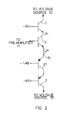
- Figure 2 is a schematic diagram of a cascode stage of the video amplifier circuit in accordance with an alternative embodiment.
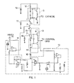
- Figure 1 is a schematic diagram of a cascode mirror high bandwidth video amplifier in accordance with the preferred embodiment. The circuit is so named because it comprises two amplifiers, each being the mirror image of the other. The first such amplifier includes a cascode
stage comprising transistors output stage 5. Likewise, the mirror image amplifier includes a cascode stage comprising transistor 3 (transistor 3 being common to the cascode stages of both amplifiers) and an output stage 9. - According to the illustrated preferred embodiment,
transistors transistor 7 is a PNP bipolar transistor. However,transistors - Operating current flows through the mirror image amplifiers from a first source of
DC power 10 through pull upresistor 12, and flows out of the mirror image amplifiers through further pull-up resistor 14 to a second DC power source. According to a successful prototype,power source 10 delivers +85 volts whilesource 16 delivers -85 volts of DC power to the mirror image amplifier pair. - The aforementioned cascode stages function as transconductance amplifiers for controlling the voltage gain of the entire video amplifier circuit. The
output stages 5 and 9, on the other hand, function to isolate the load capacitance of the CRT from the respective cascode stages in order that a sufficiently wide bandwidth can be achieved. - A
preamplifier 11 is provided for receiving and level adjusting an input video signal according to the output of afeedback clamping network 13. The function of thefeedback clamping network 13 is to sample the video output signal applied to the control grid for effecting DC adjustment of the preamplified input signal output frompreamplifier 11. The construction and operation of thepreamplifier 11 andfeedback clamping network 13 are not described in detail herein, but are believed to be well within the expected knowledge of a person skilled in the art to which the present invention pertains. - Operation of the invention will be described with reference to the first of the aforementioned mirror image amplifiers. As discussed above, the cascode stage comprises a common-
emitter amplifier 3 connected in series with a common-base amplifier 1, each amplifier comprising a bipolar junction transistor. The transconductance (gm) of thecommon emitter amplifier 3 is 1/(R15+re), where re is the emitter-ballast resistance of thecommon emitter transistor external resistor 15 connected to the emitter oftransistor 3, in a well known manner. - A base terminal of
transistor 1 is connected to a source ofbias voltage 17 such that the transistor operates as a current buffer. Thus, the gain of the cascode stage is essentially the same as that of thecommon emitter transistor 3, and thus equals -gmR12, where R12 is the resistance of pull-upresistor 12. - The cascode configuration of
transistors emitter resistor 15, and exhibiting a value of resistance close to R15 and an RC constant equal to a few nanoseconds. Furthermore, the addition of a peaking coil (not shown) to the collector terminal ofcommon base transistor 1 can further improve the transition times. - The cascode stage for the mirror image amplifier comprises
transistors DC power source 16 via pull-up resistor 14, as described above. Because this latter amplifier is a mirror image of the above-discussed amplifier, its operation is identical. - As discussed above, each of the mirror image amplifiers include
respective output stage 5 and 9 in the form of emitter-followers which are biased at the Class B operating point. According to the preferred embodiment, a pair of diodes are used for providing typically no more that 0.6 volts of bias to the emitter-follower transistor configuration in order to maintain the above discussed Class B operating point. However, in the event that high frequency transitions are required at the output stage, more current is typically drawn so that the emitter follower transistors will have a tendency to heat up. The elevated junction temperature can result in a shift from Class B bias to Class AB bias, in a well known manner. - Additional details of construction and operation of emitter
follower output stages 5 and 9 are not discussed in detail herein but would be well known to a person skilled in the art. - Considering the circuit as a whole, the two mirror image video amplifiers are cascaded together to form the complete video amplifier, with one side being powered by
DC source 10 and the other side being powered byDC source 16. As discussed above,transistor 3 functions as a transconductance amplifier for converting the preamplified input voltage signal received frompreamplifier 11 into an amplified current signal (ic) and an emitter current (ie) to the emitter terminals oftransistors transistor 3 functions as a voltage controlled current source. Sincetransistors transistor 3 appear at the collector terminals oftransistors - Consequently, the same signal current flows from
DC voltage source 10 to oppositepolarity voltage source 16 through pull-upresistors resistors follower output stages 5 and 9 to the cathode and control grid, respectively, of the CRT electron gun. - In accordance with the successful prototype, the combined voltage output results in a total signal swing amplitude of as high as 140 volts. The magnitude of the voltage signal swing depends on the biasing voltages of the
common base transistors transistors voltage sources transistor 1 and Vcb7 denotes the collector-base voltage oftransistor 7. The maximum signal current is thus (85-6-Vcb1)/R12 for linear operation. - Although Figure 1 illustrates the circuit in accordance with a preferred embodiment of the present invention, other modifications and variations are possible. For example, according to the alternative embodiment of Figure 2, an additional PNP transistor is shown connected between
emitter resistor 15 andtransistor 7, in order to obtain better symmetry between the output voltage signals. - All such modifications and variations are believed to be within the sphere and scope of the present invention as defined by the claims appended hereto.
Claims (19)
- A circuit for generating equal amplitude and opposite phase signals, comprising a pair of cascaded amplifiers connected via respective equal valued resistances to a pair of opposite polarity power sources, and a voltage controlled current source common to each said pair of amplifiers for receiving an input signal and in response generating a common current signal within each said pair of amplifiers such that equal amplitude and opposite phase voltage signals are generated across said respective resistances.
- The circuit of claim 1 wherein said pair of cascaded amplifiers comprise a pair of common-base amplifiers operating as current buffers for said common current, and said voltage controlled current source comprises a common-emitter amplifier intermediate said pair of common-base amplifiers.
- The circuit of claim 1 further comprising a pair of emitter follower stages connected to respective ones of said cascaded amplifiers.
- The circuit of claim 2 further including a peaking coil connected to respective collector terminals of said pair of common-base amplifiers for enhancing transition times of said common current signal.
- The circuit of claim 2 further including a transistor intermediate said common-emitter amplifier and a predetermined one of said pair of common-base amplifiers for enhancing symmetry of said common current signal.
- A video amplifier for controlling an electron source cathode and a control grid of a cathode ray tube, comprising:a) a first cascode stage connected to a first DC power source through a first pull-up resistor;b) a second cascode stage connected to a second DC power source through a second pull-up resistor;c) a voltage controlled current source common to each said first and second stages for receiving an input signal and in response generating a common current signal within each said first and second stages such that respective first and second equal amplitude and opposite phase voltage signals are generated across said first and second pull-up resistors, respectively;d) a first emitter-follower stage for receiving and applying said first voltage signal to said electron source cathode while isolating load capacitance of said cathode ray tube from said first cathode stage; ande) a second emitter-follower stage for receiving and applying said second voltage signal to said control grid while isolating load capacitance of said cathode ray tube from said second cathode stage.
- The video amplifier of claim 6 wherein said first cathode stage and said common current source respectively comprise a common-base amplifier and a common-emitter amplifier connected in series.
- The video amplifier of claim 6 wherein said second cathode stage and said common current source respectively comprise a common-base amplifier and a common-emitter amplifier connected in series.
- The video amplifier of claim 7 wherein said first emitter-follower stage is biased via diode means for operation in Class B mode, said diode means being connected to said first resistor and to a collector terminal of said common-base amplifier.
- The video amplifier of claim 8 wherein said second emitter-follower stage is biased via diode means for operation in Class B mode, said diode means being connected to said second resistor and to a collector terminal of said common-base amplifier.
- The video amplifier of claim 7, 8, 9 or 10 further comprising a source of bias voltage connected to a base terminal of said common-base amplifier.
- The video amplifier of claim 7 or 9 wherein said common-base amplifier and said common-emitter amplifier are connected via respective emitter and collector terminals thereof.
- The video amplifier of claim 8 or 10 wherein said common-base amplifier and said common-emitter amplifier are connected via respective collector and emitter terminals through a further resistor.
- The video amplifier of claim 11 wherein said source of bias voltage is 6 volts DC.
- The video amplifier of claim 11 wherein said source of bias voltage is -1 volt DC.
- The video amplifier of claim 6, 7 or 8 wherein said first and second DC power sources generate +85 volt and -85 volt DC signals respectively.
- The video amplifier of claim 7 or 8 further comprising a preamplifier for preamplifying and applying said input signal to a base terminal of said common-emitter amplifier, and a feedback clamping network for sampling said second voltage signal applied to said control grid and in response adjusting DC level of said preamplified input signal, thereby compensating for voltage drift within said video amplifier.
- The video amplifier of claim 7 or 8 further including a peaking coil connected to respective collector terminals of said common-base amplifier for enhancing transition times of said common current signal.
- The circuit of claim 7 or 8 further including a transistor intermediate said common-emitter amplifier and said common-base amplifier for enhancing symmetry of said common current signal.
Applications Claiming Priority (2)
| Application Number | Priority Date | Filing Date | Title |
|---|---|---|---|
| CA2016286 | 1990-05-08 | ||
| CA002016286A CA2016286C (en) | 1990-05-08 | 1990-05-08 | Cascode mirror video amplifier |
Publications (2)
| Publication Number | Publication Date |
|---|---|
| EP0457160A1 true EP0457160A1 (en) | 1991-11-21 |
| EP0457160B1 EP0457160B1 (en) | 1996-08-14 |
Family
ID=4144943
Family Applications (1)
| Application Number | Title | Priority Date | Filing Date |
|---|---|---|---|
| EP91107408A Expired - Lifetime EP0457160B1 (en) | 1990-05-08 | 1991-05-07 | Cascode mirror video amplifier |
Country Status (4)
| Country | Link |
|---|---|
| EP (1) | EP0457160B1 (en) |
| AT (1) | ATE141449T1 (en) |
| CA (1) | CA2016286C (en) |
| DE (1) | DE69121293T2 (en) |
Cited By (2)
| Publication number | Priority date | Publication date | Assignee | Title |
|---|---|---|---|---|
| GB2364839A (en) * | 2000-07-12 | 2002-02-06 | Teck Lee Wong | The ultra complementary audio amplifier output stage |
| CN112234945A (en) * | 2020-10-14 | 2021-01-15 | 联合微电子中心有限责任公司 | Distributed amplifier circuit, gain cell and electronic device |
Families Citing this family (1)
| Publication number | Priority date | Publication date | Assignee | Title |
|---|---|---|---|---|
| DE102008034456B4 (en) | 2008-07-24 | 2011-07-28 | Linck, Fritz, 86391 | DC coupled cascaded transistor amplifier for high output voltages |
Citations (5)
| Publication number | Priority date | Publication date | Assignee | Title |
|---|---|---|---|---|
| GB809401A (en) * | 1957-08-02 | 1959-02-25 | Mullard Ltd | Improvements in or relating to circuit arrangements employing transistors |
| GB1139744A (en) * | 1965-06-18 | 1969-01-15 | Siemens Ag | Improvements in or relating to differential amplifiers employing transistors |
| US4641063A (en) * | 1985-12-10 | 1987-02-03 | Yosif Smushkovich | Video driver level shifter |
| US4651064A (en) * | 1984-09-13 | 1987-03-17 | Sperry Corporation | Video amplifier with foreground and background controls |
| US4973890A (en) * | 1990-05-10 | 1990-11-27 | Electrohome Limited | Cascode mirror video amplifier |
-
1990
- 1990-05-08 CA CA002016286A patent/CA2016286C/en not_active Expired - Fee Related
-
1991
- 1991-05-07 AT AT91107408T patent/ATE141449T1/en not_active IP Right Cessation
- 1991-05-07 EP EP91107408A patent/EP0457160B1/en not_active Expired - Lifetime
- 1991-05-07 DE DE69121293T patent/DE69121293T2/en not_active Expired - Fee Related
Patent Citations (5)
| Publication number | Priority date | Publication date | Assignee | Title |
|---|---|---|---|---|
| GB809401A (en) * | 1957-08-02 | 1959-02-25 | Mullard Ltd | Improvements in or relating to circuit arrangements employing transistors |
| GB1139744A (en) * | 1965-06-18 | 1969-01-15 | Siemens Ag | Improvements in or relating to differential amplifiers employing transistors |
| US4651064A (en) * | 1984-09-13 | 1987-03-17 | Sperry Corporation | Video amplifier with foreground and background controls |
| US4641063A (en) * | 1985-12-10 | 1987-02-03 | Yosif Smushkovich | Video driver level shifter |
| US4973890A (en) * | 1990-05-10 | 1990-11-27 | Electrohome Limited | Cascode mirror video amplifier |
Non-Patent Citations (1)
| Title |
|---|
| INSTRUMENTS AND EXPERIMENTAL TECHNIQUES. no. 3, May 1968, NEW YORK US pages 614 - 615; S.R. IVANOV ET AL: 'High-Voltage Transistor Paraphase Amplifier ' * |
Cited By (3)
| Publication number | Priority date | Publication date | Assignee | Title |
|---|---|---|---|---|
| GB2364839A (en) * | 2000-07-12 | 2002-02-06 | Teck Lee Wong | The ultra complementary audio amplifier output stage |
| CN112234945A (en) * | 2020-10-14 | 2021-01-15 | 联合微电子中心有限责任公司 | Distributed amplifier circuit, gain cell and electronic device |
| CN112234945B (en) * | 2020-10-14 | 2024-02-27 | 联合微电子中心有限责任公司 | Distributed amplifier circuit, gain unit and electronic device |
Also Published As
| Publication number | Publication date |
|---|---|
| CA2016286A1 (en) | 1991-11-08 |
| EP0457160B1 (en) | 1996-08-14 |
| DE69121293D1 (en) | 1996-09-19 |
| CA2016286C (en) | 1998-02-10 |
| ATE141449T1 (en) | 1996-08-15 |
| DE69121293T2 (en) | 1997-03-06 |
Similar Documents
| Publication | Publication Date | Title |
|---|---|---|
| KR940020822A (en) | Circuit to compensate for blue phosphor roll off at high drive level in projection television system | |
| US4973890A (en) | Cascode mirror video amplifier | |
| JPH0550163B2 (en) | ||
| JPS62219777A (en) | Gumma correction circuit | |
| US5469106A (en) | Voltage controlled amplifier which reduces differential gain | |
| EP0457160B1 (en) | Cascode mirror video amplifier | |
| US4318052A (en) | Wideband high voltage video amplifier | |
| US5578966A (en) | Output stage for a high-speed video amplifier | |
| US20050127999A1 (en) | Low distortion and high slew rate output stage for voltage feedback amplifier | |
| US5293101A (en) | Driving circuit apparatus for CRT | |
| US5376900A (en) | Push-pull output stage for amplifier in integrated circuit form | |
| JPS58103207A (en) | Power supply circuit of amplifier | |
| US4654712A (en) | High frequency wide bandwith video amplifier with high tracking linearity | |
| JP3322890B2 (en) | Gamma offset adjustment circuit | |
| KR100345435B1 (en) | Picture display apparatus with beam scan velocity modulation | |
| JP2796348B2 (en) | Output circuit | |
| JP2973910B2 (en) | Circuit for adjusting signal coring threshold | |
| JPH057805Y2 (en) | ||
| RU2156537C1 (en) | Linear power amplifier | |
| JP3235745B2 (en) | Gain control amplifier circuit and primary color signal amplifier | |
| JPH0443442B2 (en) | ||
| US5266853A (en) | Peak clipper with an expanded linear characteristic region for video signals | |
| JPH0753105Y2 (en) | Vertical raster centering circuit | |
| JPH0450700Y2 (en) | ||
| US5452020A (en) | Cathode ray tube driver with input black tracking provisions |
Legal Events
| Date | Code | Title | Description |
|---|---|---|---|
| PUAI | Public reference made under article 153(3) epc to a published international application that has entered the european phase |
Free format text: ORIGINAL CODE: 0009012 |
|
| AK | Designated contracting states |
Kind code of ref document: A1 Designated state(s): AT BE CH DE DK ES FR GB GR IT LI LU NL SE |
|
| 17P | Request for examination filed |
Effective date: 19920513 |
|
| 17Q | First examination report despatched |
Effective date: 19950203 |
|
| GRAH | Despatch of communication of intention to grant a patent |
Free format text: ORIGINAL CODE: EPIDOS IGRA |
|
| GRAA | (expected) grant |
Free format text: ORIGINAL CODE: 0009210 |
|
| AK | Designated contracting states |
Kind code of ref document: B1 Designated state(s): AT BE CH DE DK ES FR GB GR IT LI LU NL SE |
|
| PG25 | Lapsed in a contracting state [announced via postgrant information from national office to epo] |
Ref country code: NL Free format text: LAPSE BECAUSE OF FAILURE TO SUBMIT A TRANSLATION OF THE DESCRIPTION OR TO PAY THE FEE WITHIN THE PRESCRIBED TIME-LIMIT Effective date: 19960814 Ref country code: LI Effective date: 19960814 Ref country code: GR Free format text: LAPSE BECAUSE OF FAILURE TO SUBMIT A TRANSLATION OF THE DESCRIPTION OR TO PAY THE FEE WITHIN THE PRESCRIBED TIME-LIMIT Effective date: 19960814 Ref country code: ES Free format text: THE PATENT HAS BEEN ANNULLED BY A DECISION OF A NATIONAL AUTHORITY Effective date: 19960814 Ref country code: DK Effective date: 19960814 Ref country code: CH Effective date: 19960814 Ref country code: BE Effective date: 19960814 Ref country code: AT Effective date: 19960814 |
|
| REF | Corresponds to: |
Ref document number: 141449 Country of ref document: AT Date of ref document: 19960815 Kind code of ref document: T |
|
| REF | Corresponds to: |
Ref document number: 69121293 Country of ref document: DE Date of ref document: 19960919 |
|
| ITF | It: translation for a ep patent filed | ||
| PG25 | Lapsed in a contracting state [announced via postgrant information from national office to epo] |
Ref country code: SE Effective date: 19961114 |
|
| ET | Fr: translation filed | ||
| NLV1 | Nl: lapsed or annulled due to failure to fulfill the requirements of art. 29p and 29m of the patents act | ||
| REG | Reference to a national code |
Ref country code: CH Ref legal event code: PL |
|
| PGFP | Annual fee paid to national office [announced via postgrant information from national office to epo] |
Ref country code: GB Payment date: 19970507 Year of fee payment: 7 |
|
| PGFP | Annual fee paid to national office [announced via postgrant information from national office to epo] |
Ref country code: FR Payment date: 19970529 Year of fee payment: 7 |
|
| PG25 | Lapsed in a contracting state [announced via postgrant information from national office to epo] |
Ref country code: LU Free format text: LAPSE BECAUSE OF NON-PAYMENT OF DUE FEES Effective date: 19970531 |
|
| PLBE | No opposition filed within time limit |
Free format text: ORIGINAL CODE: 0009261 |
|
| STAA | Information on the status of an ep patent application or granted ep patent |
Free format text: STATUS: NO OPPOSITION FILED WITHIN TIME LIMIT |
|
| PGFP | Annual fee paid to national office [announced via postgrant information from national office to epo] |
Ref country code: DE Payment date: 19970729 Year of fee payment: 7 |
|
| 26N | No opposition filed | ||
| PG25 | Lapsed in a contracting state [announced via postgrant information from national office to epo] |
Ref country code: GB Free format text: LAPSE BECAUSE OF NON-PAYMENT OF DUE FEES Effective date: 19980507 |
|
| PG25 | Lapsed in a contracting state [announced via postgrant information from national office to epo] |
Ref country code: FR Free format text: LAPSE BECAUSE OF NON-PAYMENT OF DUE FEES Effective date: 19980531 |
|
| GBPC | Gb: european patent ceased through non-payment of renewal fee |
Effective date: 19980507 |
|
| PG25 | Lapsed in a contracting state [announced via postgrant information from national office to epo] |
Ref country code: DE Free format text: LAPSE BECAUSE OF NON-PAYMENT OF DUE FEES Effective date: 19990302 |
|
| REG | Reference to a national code |
Ref country code: FR Ref legal event code: ST |
|
| PG25 | Lapsed in a contracting state [announced via postgrant information from national office to epo] |
Ref country code: IT Free format text: LAPSE BECAUSE OF NON-PAYMENT OF DUE FEES;WARNING: LAPSES OF ITALIAN PATENTS WITH EFFECTIVE DATE BEFORE 2007 MAY HAVE OCCURRED AT ANY TIME BEFORE 2007. THE CORRECT EFFECTIVE DATE MAY BE DIFFERENT FROM THE ONE RECORDED. Effective date: 20050507 |