EP0454566B1 - Laser compact à semi-conducteur du type à pompage électronique - Google Patents
Laser compact à semi-conducteur du type à pompage électronique Download PDFInfo
- Publication number
- EP0454566B1 EP0454566B1 EP91401070A EP91401070A EP0454566B1 EP 0454566 B1 EP0454566 B1 EP 0454566B1 EP 91401070 A EP91401070 A EP 91401070A EP 91401070 A EP91401070 A EP 91401070A EP 0454566 B1 EP0454566 B1 EP 0454566B1
- Authority
- EP
- European Patent Office
- Prior art keywords
- laser
- semiconductor
- zone
- laser according
- electron source
- Prior art date
- Legal status (The legal status is an assumption and is not a legal conclusion. Google has not performed a legal analysis and makes no representation as to the accuracy of the status listed.)
- Expired - Lifetime
Links
Images


Classifications
-
- H—ELECTRICITY
- H01—ELECTRIC ELEMENTS
- H01S—DEVICES USING THE PROCESS OF LIGHT AMPLIFICATION BY STIMULATED EMISSION OF RADIATION [LASER] TO AMPLIFY OR GENERATE LIGHT; DEVICES USING STIMULATED EMISSION OF ELECTROMAGNETIC RADIATION IN WAVE RANGES OTHER THAN OPTICAL
- H01S5/00—Semiconductor lasers
- H01S5/20—Structure or shape of the semiconductor body to guide the optical wave ; Confining structures perpendicular to the optical axis, e.g. index or gain guiding, stripe geometry, broad area lasers, gain tailoring, transverse or lateral reflectors, special cladding structures, MQW barrier reflection layers
-
- H—ELECTRICITY
- H01—ELECTRIC ELEMENTS
- H01J—ELECTRIC DISCHARGE TUBES OR DISCHARGE LAMPS
- H01J1/00—Details of electrodes, of magnetic control means, of screens, or of the mounting or spacing thereof, common to two or more basic types of discharge tubes or lamps
- H01J1/02—Main electrodes
- H01J1/30—Cold cathodes, e.g. field-emissive cathode
- H01J1/304—Field-emissive cathodes
- H01J1/3042—Field-emissive cathodes microengineered, e.g. Spindt-type
-
- H—ELECTRICITY
- H01—ELECTRIC ELEMENTS
- H01S—DEVICES USING THE PROCESS OF LIGHT AMPLIFICATION BY STIMULATED EMISSION OF RADIATION [LASER] TO AMPLIFY OR GENERATE LIGHT; DEVICES USING STIMULATED EMISSION OF ELECTROMAGNETIC RADIATION IN WAVE RANGES OTHER THAN OPTICAL
- H01S3/00—Lasers, i.e. devices using stimulated emission of electromagnetic radiation in the infrared, visible or ultraviolet wave range
- H01S3/09—Processes or apparatus for excitation, e.g. pumping
- H01S3/0955—Processes or apparatus for excitation, e.g. pumping using pumping by high energy particles
- H01S3/0959—Processes or apparatus for excitation, e.g. pumping using pumping by high energy particles by an electron beam
-
- H—ELECTRICITY
- H01—ELECTRIC ELEMENTS
- H01S—DEVICES USING THE PROCESS OF LIGHT AMPLIFICATION BY STIMULATED EMISSION OF RADIATION [LASER] TO AMPLIFY OR GENERATE LIGHT; DEVICES USING STIMULATED EMISSION OF ELECTROMAGNETIC RADIATION IN WAVE RANGES OTHER THAN OPTICAL
- H01S5/00—Semiconductor lasers
- H01S5/04—Processes or apparatus for excitation, e.g. pumping, e.g. by electron beams
-
- H—ELECTRICITY
- H01—ELECTRIC ELEMENTS
- H01S—DEVICES USING THE PROCESS OF LIGHT AMPLIFICATION BY STIMULATED EMISSION OF RADIATION [LASER] TO AMPLIFY OR GENERATE LIGHT; DEVICES USING STIMULATED EMISSION OF ELECTROMAGNETIC RADIATION IN WAVE RANGES OTHER THAN OPTICAL
- H01S5/00—Semiconductor lasers
- H01S5/20—Structure or shape of the semiconductor body to guide the optical wave ; Confining structures perpendicular to the optical axis, e.g. index or gain guiding, stripe geometry, broad area lasers, gain tailoring, transverse or lateral reflectors, special cladding structures, MQW barrier reflection layers
- H01S5/2004—Confining in the direction perpendicular to the layer structure
-
- H—ELECTRICITY
- H01—ELECTRIC ELEMENTS
- H01S—DEVICES USING THE PROCESS OF LIGHT AMPLIFICATION BY STIMULATED EMISSION OF RADIATION [LASER] TO AMPLIFY OR GENERATE LIGHT; DEVICES USING STIMULATED EMISSION OF ELECTROMAGNETIC RADIATION IN WAVE RANGES OTHER THAN OPTICAL
- H01S5/00—Semiconductor lasers
- H01S5/30—Structure or shape of the active region; Materials used for the active region
- H01S5/32—Structure or shape of the active region; Materials used for the active region comprising PN junctions, e.g. hetero- or double- heterostructures
- H01S5/3211—Structure or shape of the active region; Materials used for the active region comprising PN junctions, e.g. hetero- or double- heterostructures characterised by special cladding layers, e.g. details on band-discontinuities
Definitions
- the present invention relates to a compact semiconductor laser of the electronically pumped type. It applies in particular to all types of optical information processing; it can be used in compact disc players (audio or video), in optical memory systems, in laser printers or barcode readers. It also applies to optical recording and laboratory instrumentation.
- Three types of semiconductor lasers using semiconductor alloys as a laser cavity, exist and are distinguished by their modes of generation of the laser effect. These are injection laser diodes, electronically pumped lasers, and optically pumped lasers.
- III-V injection laser diodes The main compact commercial products that exist are III-V injection laser diodes.
- the production of laser diodes requires the use of complex technologies of doping and thin film metallurgy, which are only mastered for semiconductors of the family of III-V compounds, based on Ga, Al, In atoms. , As, P and Sb.
- the main advantage of III-V laser diodes is their compactness, that is to say their small size, of the order of cm 3 .
- III-V laser diodes are the limitations of the range of emission wavelengths between 0.6 and 1.55 micrometers, which comes from the only possibility of using III-V materials.
- pumped lasers electronics use electronic bombardment to excite the semiconductor.
- electronic pumping is carried out using an electron gun.
- An achievement is described in the article by A. Nasibov, "Laser cathode ray tubes and their applications", SPIE vol.893 High power Laser Diodes and Applications p. 200-202 (1988).
- Electron-pumped lasers are also described in the article by OV Bogdankevich et al., "Variable-gap Al x Ga 1-x As heterostructure for an electron-beam-pumped laser", Soviet Journal of Quantum Electronics, 17 (1987 ) 9, pages 1155-1156 and in the European patent application EP-A-0 119 646.
- the main advantage of these lasers is the separation of the "pumping source” and "laser cavity” functions, which allows the use of all direct gap semiconductors, and in particular those which do not allow direct injection, therefore the production of injection laser diodes.
- the use of all direct gap semiconductors makes it possible to extend the wavelength range from ultraviolet to infrared.
- the current density used is of the order of 10 to 100 A / cm 2 ; the acceleration voltage used is of the order of 20 to 100 kV.
- These high values prohibit the production of such a semiconductor laser of reduced volume (of the order of cm 3 ), and compact, having dimensions and advantages comparable to those of laser diodes III-V. Because of the high energy densities, only the pulsed operating mode is authorized, and their application is limited to the laser applied to the display.
- An object of the present invention is the production of an electronically pumped type semiconductor laser in compact form and having a reduced volume (of the order of cm 3 ), comparable to that of laser diodes III-V, and having the specific advantages of electronically pumped semiconductor lasers.
- Another object of the present invention linked to the specific advantages of electronically pumped lasers, is to authorize the production of lasers delivering light beams in a wavelength range from ultraviolet to medium infrared, and which depend on the nature of the semiconductor materials used.
- the invention achieves these goals, using, in a compact device, on the one hand a compact source of electrons, on the other hand a compact semiconductor laser cavity and of particular structure to have a threshold of current and a low electron acceleration voltage.
- the electronic excitation zone has a decreasing band gap gradient.
- the confinement zones have an index gradient.
- a low threshold current and a low acceleration voltage make it possible to considerably lower the energy densities deposited on the semiconductor. This, by simplifying the assembly of the laser device, and by using a cold source of electrons having a volume of less than cm 3 , makes it possible to obtain a compact laser, having the advantages mentioned above.
- the heterostructure is multiple. It can be composed of alloys based on Cd, Zn, Mn, Hg, Te, Se, S or other.
- the semiconductors used are of the direct gap type; they are chosen, for example, from compounds III-V and II-VI and make it possible to cover the extent of the wavelength range from the ultraviolet to the infrared.
- the semiconductor is preferably a compound II-VI.
- the semiconductor is in the form of a resonant cavity of the Fabry-Perot type, the mirrors of which are produced by cleavage, and possibly by deposition of thin optical layers in order to control the reflectivity of the mirrors.
- the resonant cavity can be of the distributed cavity type, for example distributed feedback cavity, or distributed Bragg reflector cavity.
- the active area can consist of a single well, or a quantum well, or a multi-well quantum, or a superlattice, or a combination of these structures.
- the pumping device can be chosen from cold sources of electrons with PN, PIN or Schottky junction, with a metal-insulator-metal structure with a tunnel effect, or using ferroelectric materials.
- cold sources of electrons produced by microelectronics techniques are used, which facilitates mass production of the devices.
- the pumping device is a cold source of electrons with emissive cathodes with microtips.
- These last two types of source can have a mosaic, matrix, or mosaic matrix structure.
- this electrode has a shape suitable for focusing on the semiconductor of electric field lines coming from the cold source of electrons.
- This shape can for example be conical or pyramidal, the semiconductor being arranged at the top.
- the laser comprises means for focusing along a ribbon of the electrons coming from the cold source of electrons.
- these means consist of conductive screens arranged on either side of the electron beam and having a geometry specific to the focusing.
- the laser comprises a cooling system which also allows regulation of the parameters of the light beam delivered.
- This system can for example consist of a simple radiator or a thermoelectric cooler of the Peltier effect type.
- the active material of the laser has a structure having a laser effect for an electronic threshold current density of less than 10 A / cm 2 and for an electron acceleration voltage of less than 10 kV.
- a multiple heterostructure of compound II-VI (for example CdZnTe semiconductor alloys) meets these criteria.
- Such a structure can be produced by the technique of molecular beam epitaxy.
- a deposition is carried out on a solid substrate of CdZnTe or GaAs semiconductor alloy having a particular crystalline orientation, ⁇ 100> for example.
- the surface of the substrate is approximately 1 cm 2 .
- the substrate is thinned and reduced to a thickness of between 50 and 200 micrometers.
- the “matches” are then made, that is to say rectangular semiconductor crystals, two parallel faces of which serve as mirrors to form the resonant cavity of the Fabry-Perot type of the laser. These "matches” are obtained for example by cleavage of the mirror faces and cutting with a saw of the heteroepitaxial substrate bonded to a flexible metal sheet.
- a “match” has a length between 200 and 2000 micrometers (which corresponds to the spacing between two cleavage planes) and a width between 50 and 2000 micrometers (spacing between two cutting lines with a saw).
- the mirrors of the resonant cavity of the laser are the cleavage faces.
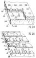
- FIGS. 1A and 1B represent the heterostructure in thin layers of the semiconductor 10 and the energy of the gap EG (zone of prohibited energy between the valence band and the conduction band of the alloy considered) of each zone in as a function of the depth P.
- the origin of the depth P is chosen in the middle of the active region of the semiconductor.
- the suitably excited heterostructure emits a laser beam centered on a wavelength between 0.55 and 0.75 micrometers.
- FIG. 1B represents the resonant cavity of the Fabry-Perot type.
- a side FD made by cutting
- a side M made by cleavage and serving as a mirror for the Fabry-Pérot.
- the structure of the laser cavity shown by way of example in FIG. 1B, is suitable for a type of gain guidance.
- Other known structures of the index guidance type can also be used.
- the semiconductor 10 is pumped by an electron bombardment produced by a cold electron source 23, for example by a network, that is to say a mosaic or a matrix or a matrix of mosaics , of microtips cathodes with cold electronic emission with field effect.
- a network that is to say a mosaic or a matrix or a matrix of mosaics , of microtips cathodes with cold electronic emission with field effect.
- the mosaic consists of a conductive layer 24 deposited on a substrate 26, which can be insulating, for example made of glass, or semiconductor, for example made of silicon, of thickness between 0.2 and 0.5 millimeter.
- This conductive layer is provided with conductive microtips 28.
- the microtips have a base diameter of about 1.5 micrometers and are spaced, for example, 3 or 10 micrometers; there are therefore for example between 10 000 and 100 000 microtips per mm 2 .
- the assembly is covered with an insulating layer 30 provided with openings allowing the microtips 28 to point outwards.
- the thickness of the insulating layer 30 is of the order of 1 micrometer.
- the insulating layer 30 is covered by a conductive layer provided with openings facing the tips 28.
- the openings have a diameter of about 1.5 micrometers. This conductive layer forms the extraction grid.
- the microtips 28 When applying adequate potentials to the conductive layers 24 and 32, the microtips 28 emit electrons by field effect.
- FIG. 2B represents a matrix variant of the microtip array, which is called a microtip array.
- the conductive layers 24 and 32 are arranged in columns and rows isolated from each other. At the intersection of each row 32 and each column 24, there may be one or more microtips.
- the microtips 28 located at the intersection of a line and a column brought to these potentials emit electrons.
- the electron emission zone By selective application of these potentials on the rows and columns, one can choose the electron emission zone.
- the electron density emitted is a function of the values of the potentials applied.
- the current density can range from 1 to 10 mA / mm 2 .
- the current emitted is for example between 0.1 and 5 mA.
- the total current depends on the one hand on the applied potentials, on the other hand on the number and the density of the microtips as well as on the surface of the network of microtips.
- the network has for example a rectangular surface of between 0.1 and 0.5 mm 2 .
- the cold electron source 23 can also be constituted by a network of emitters with silicon cathodes.
- Figure 3 shows schematically in section such a transmitter. A complete description of such transmitters can be found, for example, in the article by G.G.P. Van Gorkom and M. Moeberechts, Philips Technical Review, vol. 43, n ° 3, p. 49-57 (1987).
- An epitaxial layer 27 of p-type Si 6 micrometers thick rests on a p + type Si substrate 400 micrometers thick.
- phosphorus is diffuse to form a layer 29 of type n + 3 microns thick.
- the cylindrical active zone 31, of diameter d less than 10 micrometers, of type p + is produced by implantation of boron. Its typical concentration is 5 x 10 1 7 cm -3 .
- the emission zone corresponding to the PN junction, at the interface of the zones referenced 31 and 33, has a cylindrical symmetry, and a diameter of less than 10 micrometers.
- the assembly produces two diodes with P-N junctions, constituted respectively by the zones referenced 27, 29 and 31, 33, connected in parallel.
- An insulator 35 for example made of SiO 2 , 1 micrometer thick, forming a cylindrical stud, on which a conductive layer 39, 0.5 micrometer thick, for example aluminum, rests, to screen the electric fields, limit the loading of the insulation, and possibly serve as an electrode in an electronic optical system.
- the PN junctions are polarized in reverse, using the voltage Vd.
- a very strong electric field of the order of 10 6 V / cm, is created.
- This strong field in the depletion zone of the diode produced by the junction p + / n ++ of the zones 31, 33 accelerates the electrons from the zone p + 31 towards the zone n ++ 33.
- These accelerated “hot” electrons create an "avalanche effect", creating, by collision with the valence electrons, other electron-hole pairs.
- Vd is typically between 6 and 9 V.
- the current of the diode is a few mA.
- the current density, and the electronic emission current, for a diameter of 1 micrometer are respectively 1,500 A / cm 2 and 10 microamperes.
- a monoatomic layer of cesium is deposited on the surface.
- the emission current varies between 10 microamperes and 60 microamperes.
- the manufacturing methods use microelectronic technology, and make it possible to manufacture chips comprising several cathodes forming an array.
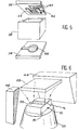
- the semiconductor 10, cut and processed as indicated above, is held facing the cold source of electrons 23, for example a network of microtip cathodes, at a determined distance, for example between 1 and 10 mm.
- the pumping is transverse and the semiconductor 10 emits a laser beam by one of its faces parallel to the plane of the sheet, support of the figure.
- the assembly formed by the semiconductor 10 and the pumping device 23 is maintained in an enclosure 34 under secondary vacuum.
- This enclosure 34 is produced by a microtube 36 for example with rectangular faces closed on two opposite sides by two plates of insulating material 26, 38 made of glass, for example.
- the enclosure 34 has at least one window transparent to the wavelength of the laser beam.
- the microtube 36 is made of optical quality glass and therefore plays the role of window.
- the plates 26, 38 are welded to the microtube 36 by welds 37, for example in fusible glass, by means of local heating by laser, or other heating.
- the network 23 is for example directly produced on a plate 26.
- conductive tracks 40 made of copper for example, allow the polarization of the conductors of the network 23.
- An additional conductive track 42 of the geometry suitable allows the attachment and polarization of focusing means 44, 46.
- the plate 26 projects from the microtube 36 so as to allow electrical connection to the conductive tracks 40, 42.
- the focusing means consist of two conductive screens 44, 46, made of copper for example, welded on the conductive track 42 on either side of the network 23.
- a conductive track 48 for example made of copper, is deposited on the other plate 38.
- This track 48 allows the welding of an electrode 50, for example made of copper.
- This electrode 50 maintains the semiconductor 10 at a determined distance and facing the network 23.
- the electrode 50 has a geometry suitable for focusing on the semiconductor 10 the electric field lines coming from the network 23.
- the electrode 50 has the shape of a cone; the substrate of the semiconductor 10 is bonded with indium for example, at the top of this cone; the epitaxial layers are therefore opposite the network 23.
- the electrode 50 may also have the shape of a pyramid or any other shape allowing the focusing of the field lines.
- the electrode 50 also allows the evacuation of the heat stored in the semiconductor 10 during the electronic bombardment.
- the plate 38 extends beyond the microtube 36 so as to allow electrical connection to the track 48.
- the different elements are assembled under secondary vacuum.
- the whole is steamed (under vacuum) at a temperature between 150 ° C and 200 ° C.
- the plate 26 provided with the network 23 and the screens 44, 46 is steamed separately at a higher temperature.
- the plates 26 and 38 are positioned relative to each other by an optical method.
- the laser comprises a cooling device 52 comprising a copper radiator 54, on the one hand in contact with the external face of the plate 38 and on the other hand, in contact with a miniature effect thermoelectric cooler 56 Peltier.
- the temperature inside the enclosure 34 can be regulated but also controlled. However, we know that the laser emission wavelength depends on the temperature. It is thus possible to slightly vary or stabilize the emission wavelength by varying or stabilizing the temperature of the enclosure 34 and of the semiconductor 10.
- the cooling allows also to evacuate the excess heat which can be deposited by the electronic excitation.
- FIG. 6 schematically represents a partial view of the device of FIG. 4.
- the focusing screens 44, 46 are arranged on either side of the network 23 and of the semiconductor 10. They have a geometry adapted to the focusing of the electrons on a strip 58 of the surface of the semiconductor 10 when they are brought to an adequate potential. This makes it possible to control the width of the excitation ribbon, and therefore to control the surface and also the density of electronic excitation current; this focusing control thus makes it possible to obtain sufficiently high current densities, beyond the generation threshold of the laser beam, while keeping low currents, and low deposited energy.
- these screens 44, 46 are trapezoidal.
- the microtips are grounded.
- the gates 32 are polarized between 0 and 150 V.
- the gate potential controls the current of electrons.
- the emission of electrons is caused by an electric field of about 10 7 V / cm at the microtips.
- the screens 44, 46 are polarized between -500 and +500 V.
- the semiconductor is polarized at a positive potential value of between 3 and 10 kV.
- Field lines created by the potential difference between the grids 32 and the semiconductor 10 converge the electrons emitted by the microdots on a rectangular surface of the semiconductor 10.
- the laser cavity thus defined has a length of between 200 and 500 micrometers (length of the "match" of semiconductor alloy) and a width of between 10 and 300 micrometers (with focusing by screens 44, 46). This width depends on the focusing of the beam, which depends on the shape of the screens 44, 46, and the potentials applied.
- the guiding structure is of the gain guiding type, that is to say that the laser light will be confined in the zone defined by the excitation ribbon 58.
- the electrons arriving on the surface of the semiconductor 10 penetrate little in the surface layer (in a thickness lower than the micron). They create electron-hole pairs with a maximum yield of around 30%.
- the gap gradient (zones 12 and 14, fig. 1) causes carriers to migrate to the active zone (referenced 16, fig. 1) where they are confined. The recombination of the carriers gives rise to a light whose wavelength depends on the characteristics of the alloys and on the structure constituting the active area.
- the laser effect is obtained for a threshold of current density less than 10 A / cm 2 .
- the laser beam is delivered through one face of the microtube 36.
- the power deposited by electronic bombardment is less than around 10 kW / cm 2 , a large part of which is transformed into heat. This is evacuated by the electrode 50 to the outside.
- FIG. 7 schematically represents a section of a laser according to the invention but of which pumping is longitudinal.
- the components identical to those of FIG. 4 bear the same references.
- the electrode 60 which supports the semiconductor 10 is pierced with a tunnel 64 (it can also be hollow) opening onto the plate 62 closing the microtube 36.
- the conductive track 48 has a geometry such that it does not close the exit of tunnel 64.
- the plate 62 is made of insulating material and transparent to the wavelength of the laser beam. It must be of optical quality.
- the facing faces of the semiconductor 10 act as mirrors producing the resonant cavity of the laser.
- the mirrors are produced by depositing thin optical layers.
- FIG. 8 schematically shows in section another embodiment of a laser according to the invention.
- the components identical to those of FIG. 4 bear the same references.
- the laser comprises three semiconductors 10a, 10b, 10c of identical or different structures and capable of emitting laser beams of identical or different wavelengths.
- These three semiconductors 10a, 10b, 10c are respectively fixed to the top of three electrodes 50a, 50b, 50c which keep them at a determined distance and facing the matrix 23 of microtip cathodes.
- a laser according to the invention occupies only a reduced volume which can be of the order of cm 3 . It is compact and does not require a large power supply.
- the use of a microtip cathode network as a pumping device allows continuous, pulsed or modulated uses. To do this, it suffices to adequately control the conductors of the network.
- the invention is in no way limited to the embodiments described and shown; it admits all variants.
- the semiconductor can also be manufactured in other alloys, other heterostructures, in solid material or in thin layers.
- the cavity can be of the Fabry-Perot or distributed type, the guiding structure can be of the gain or the index type.
- the focusing electrodes and their number can be changed.
- the device can operate in continuous, pulsed or modulated mode, between 77 and 300 K, or around room temperature.
Applications Claiming Priority (2)
| Application Number | Priority Date | Filing Date | Title |
|---|---|---|---|
| FR9005268 | 1990-04-25 | ||
| FR9005268A FR2661566B1 (fr) | 1990-04-25 | 1990-04-25 | Laser compact a semi-conducteur du type a pompage electronique. |
Publications (2)
| Publication Number | Publication Date |
|---|---|
| EP0454566A1 EP0454566A1 (fr) | 1991-10-30 |
| EP0454566B1 true EP0454566B1 (fr) | 1996-07-03 |
Family
ID=9396071
Family Applications (1)
| Application Number | Title | Priority Date | Filing Date |
|---|---|---|---|
| EP91401070A Expired - Lifetime EP0454566B1 (fr) | 1990-04-25 | 1991-04-23 | Laser compact à semi-conducteur du type à pompage électronique |
Country Status (6)
| Country | Link |
|---|---|
| US (1) | US5125000A (ja) |
| EP (1) | EP0454566B1 (ja) |
| JP (1) | JP3192164B2 (ja) |
| DE (1) | DE69120595T2 (ja) |
| FR (1) | FR2661566B1 (ja) |
| NO (1) | NO911603L (ja) |
Families Citing this family (9)
| Publication number | Priority date | Publication date | Assignee | Title |
|---|---|---|---|---|
| EP0720199B1 (en) * | 1991-02-01 | 1999-06-23 | Fujitsu Limited | Field emission microcathode array devices |
| US5227699A (en) * | 1991-08-16 | 1993-07-13 | Amoco Corporation | Recessed gate field emission |
| FR2690005B1 (fr) * | 1992-04-10 | 1994-05-20 | Commissariat A Energie Atomique | Canon a electrons compact comportant une source d'electrons a micropointes et laser a semi-conducteur utilisant ce canon pour le pompage electronique. |
| FR2690286A1 (fr) * | 1992-04-17 | 1993-10-22 | Commissariat Energie Atomique | Cavité laser à hétérostructure semi-conductrice dissymétrique et laser équipé de cette cavité. |
| JP3462514B2 (ja) * | 1992-09-16 | 2003-11-05 | 住友電気工業株式会社 | 固体レーザ |
| RU2056665C1 (ru) * | 1992-12-28 | 1996-03-20 | Научно-производственное объединение "Принсипиа оптикс" | Лазерная электронно-лучевая трубка |
| US5488619A (en) * | 1994-10-06 | 1996-01-30 | Trw Inc. | Ultracompact Q-switched microlasers and related method |
| US9184559B2 (en) * | 2010-11-10 | 2015-11-10 | Ushio Denki Kabushiki Kaisha | Electron-beam-pumped light source |
| US10056735B1 (en) * | 2016-05-23 | 2018-08-21 | X Development Llc | Scanning UV light source utilizing semiconductor heterostructures |
Citations (1)
| Publication number | Priority date | Publication date | Assignee | Title |
|---|---|---|---|---|
| EP0316214A1 (fr) * | 1987-11-06 | 1989-05-17 | Commissariat A L'energie Atomique | Source d'électrons à cathodes émissives à micropointes et dispositif de visualisation par cathodoluminescence excitée par émission de champ, utilisant cette source |
Family Cites Families (8)
| Publication number | Priority date | Publication date | Assignee | Title |
|---|---|---|---|---|
| US3803510A (en) * | 1972-09-27 | 1974-04-09 | Rca Corp | Electron-beam pumped laser with extended life |
| US3942132A (en) * | 1974-09-06 | 1976-03-02 | The United States Of America As Represented By The Secretary Of The Army | Combined electron beam semiconductor modulator and junction laser |
| US4328443A (en) * | 1980-03-11 | 1982-05-04 | Avco Everett Research Laboratory, Inc. | Apparatus for providing improved characteristics of a broad area electron beam |
| US4513308A (en) * | 1982-09-23 | 1985-04-23 | The United States Of America As Represented By The Secretary Of The Navy | p-n Junction controlled field emitter array cathode |
| NL8300631A (nl) * | 1983-02-21 | 1984-09-17 | Philips Nv | Inrichting voor het opwekken van coherente straling. |
| NL8701497A (nl) * | 1987-06-26 | 1989-01-16 | Philips Nv | Halfgeleiderinrichting voor het opwekken van electromagnetische straling. |
| JPH0738438B2 (ja) * | 1988-05-27 | 1995-04-26 | 工業技術院長 | 冷電子放出型能動素子及びその製造方法 |
| JP2548352B2 (ja) * | 1989-01-17 | 1996-10-30 | 松下電器産業株式会社 | 発光素子およびその製造方法 |
-
1990
- 1990-04-25 FR FR9005268A patent/FR2661566B1/fr not_active Expired - Fee Related
-
1991
- 1991-04-04 US US07/680,322 patent/US5125000A/en not_active Expired - Lifetime
- 1991-04-23 DE DE69120595T patent/DE69120595T2/de not_active Expired - Fee Related
- 1991-04-23 NO NO91911603A patent/NO911603L/no unknown
- 1991-04-23 EP EP91401070A patent/EP0454566B1/fr not_active Expired - Lifetime
- 1991-04-24 JP JP12238591A patent/JP3192164B2/ja not_active Expired - Fee Related
Patent Citations (1)
| Publication number | Priority date | Publication date | Assignee | Title |
|---|---|---|---|---|
| EP0316214A1 (fr) * | 1987-11-06 | 1989-05-17 | Commissariat A L'energie Atomique | Source d'électrons à cathodes émissives à micropointes et dispositif de visualisation par cathodoluminescence excitée par émission de champ, utilisant cette source |
Also Published As
| Publication number | Publication date |
|---|---|
| FR2661566A1 (fr) | 1991-10-31 |
| NO911603L (no) | 1991-10-28 |
| JP3192164B2 (ja) | 2001-07-23 |
| NO911603D0 (no) | 1991-04-23 |
| DE69120595T2 (de) | 1997-01-23 |
| EP0454566A1 (fr) | 1991-10-30 |
| DE69120595D1 (de) | 1996-08-08 |
| JPH05275794A (ja) | 1993-10-22 |
| FR2661566B1 (fr) | 1995-03-31 |
| US5125000A (en) | 1992-06-23 |
Similar Documents
| Publication | Publication Date | Title |
|---|---|---|
| EP0566494B1 (fr) | Cavité laser à hétérostructure semi-conductrice dissymétrique à pompage électronique | |
| CA2232585A1 (fr) | Laser semiconducteur a emission de surface | |
| JPH02114591A (ja) | 広バンドギャップ半導体発光装置 | |
| EP0454566B1 (fr) | Laser compact à semi-conducteur du type à pompage électronique | |
| EP1138101B1 (fr) | Laser de type semi-conducteur | |
| EP0589030B1 (fr) | Canon a electrons compact comportant une source d'electrons a micropointes et laser a semi-conducteur utilisant ce canon pour le pompage electronique | |
| WO2017207898A2 (fr) | Photocathode à nanofils et méthode de fabrication d'une telle photocathode | |
| JP2003332694A (ja) | 半導体レーザ | |
| EP0993088B1 (fr) | Laser à semiconducteur, à spectre de gain accordable | |
| EP0494013A1 (fr) | Procédé de réalisation de lasers semiconducteurs à émission de surface et lasers obtenus par le procédé | |
| US5317583A (en) | Semiconductor laser screen of a cathode-ray tube | |
| EP0914699B1 (fr) | Laser comprenant un empilement de diodes laser epitaxiees compris entre deux miroirs de bragg | |
| EP0001952B1 (fr) | Diode émettrice et réceptrice de rayons lumineux de même longueur d'onde prédéterminée | |
| US6504859B1 (en) | Light sources based on semiconductor current filaments | |
| US9601895B2 (en) | Ultra fast semiconductor laser | |
| JP2002335008A (ja) | 半導体発光装置及びその製造方法 | |
| WO2023275320A1 (fr) | Composant optoelectronique insensibles aux dislocations | |
| FR3115613A1 (fr) | Dispositif de génération de photons uniques et de paires de photons intriqués | |
| FR2696278A1 (fr) | Dispositif comprenant des moyens d'injection de porteurs électroniques dans des matériaux à grand gap. | |
| FR3074372A1 (fr) | Structure a gain, dispositif photonique comprenant une telle structure et procede de fabrication d'une telle structure a gain | |
| FR2933542A1 (fr) | Dispositif a cascades quantiques a injecteur haut | |
| FR2854984A1 (fr) | Dispositif semi-conducteur d'emission d'electrons dans le vide |
Legal Events
| Date | Code | Title | Description |
|---|---|---|---|
| PUAI | Public reference made under article 153(3) epc to a published international application that has entered the european phase |
Free format text: ORIGINAL CODE: 0009012 |
|
| AK | Designated contracting states |
Kind code of ref document: A1 Designated state(s): CH DE GB IT LI NL SE |
|
| 17P | Request for examination filed |
Effective date: 19920410 |
|
| 17Q | First examination report despatched |
Effective date: 19931014 |
|
| GRAH | Despatch of communication of intention to grant a patent |
Free format text: ORIGINAL CODE: EPIDOS IGRA |
|
| GRAA | (expected) grant |
Free format text: ORIGINAL CODE: 0009210 |
|
| AK | Designated contracting states |
Kind code of ref document: B1 Designated state(s): CH DE GB IT LI NL SE |
|
| REF | Corresponds to: |
Ref document number: 69120595 Country of ref document: DE Date of ref document: 19960808 |
|
| ITF | It: translation for a ep patent filed |
Owner name: JACOBACCI & PERANI S.P.A. |
|
| GBT | Gb: translation of ep patent filed (gb section 77(6)(a)/1977) |
Effective date: 19960910 |
|
| NLR4 | Nl: receipt of corrected translation in the netherlands language at the initiative of the proprietor of the patent | ||
| PGFP | Annual fee paid to national office [announced via postgrant information from national office to epo] |
Ref country code: SE Payment date: 19970321 Year of fee payment: 7 |
|
| PGFP | Annual fee paid to national office [announced via postgrant information from national office to epo] |
Ref country code: CH Payment date: 19970416 Year of fee payment: 7 |
|
| PGFP | Annual fee paid to national office [announced via postgrant information from national office to epo] |
Ref country code: NL Payment date: 19970425 Year of fee payment: 7 |
|
| PLBE | No opposition filed within time limit |
Free format text: ORIGINAL CODE: 0009261 |
|
| STAA | Information on the status of an ep patent application or granted ep patent |
Free format text: STATUS: NO OPPOSITION FILED WITHIN TIME LIMIT |
|
| 26N | No opposition filed | ||
| PG25 | Lapsed in a contracting state [announced via postgrant information from national office to epo] |
Ref country code: SE Free format text: LAPSE BECAUSE OF NON-PAYMENT OF DUE FEES Effective date: 19980424 |
|
| PG25 | Lapsed in a contracting state [announced via postgrant information from national office to epo] |
Ref country code: LI Free format text: LAPSE BECAUSE OF NON-PAYMENT OF DUE FEES Effective date: 19980430 Ref country code: CH Free format text: LAPSE BECAUSE OF NON-PAYMENT OF DUE FEES Effective date: 19980430 |
|
| PG25 | Lapsed in a contracting state [announced via postgrant information from national office to epo] |
Ref country code: NL Free format text: LAPSE BECAUSE OF NON-PAYMENT OF DUE FEES Effective date: 19981101 |
|
| REG | Reference to a national code |
Ref country code: CH Ref legal event code: PL |
|
| NLV4 | Nl: lapsed or anulled due to non-payment of the annual fee |
Effective date: 19981101 |
|
| EUG | Se: european patent has lapsed |
Ref document number: 91401070.7 |
|
| REG | Reference to a national code |
Ref country code: GB Ref legal event code: IF02 |
|
| PGFP | Annual fee paid to national office [announced via postgrant information from national office to epo] |
Ref country code: GB Payment date: 20040421 Year of fee payment: 14 |
|
| PGFP | Annual fee paid to national office [announced via postgrant information from national office to epo] |
Ref country code: DE Payment date: 20040503 Year of fee payment: 14 |
|
| PG25 | Lapsed in a contracting state [announced via postgrant information from national office to epo] |
Ref country code: IT Free format text: LAPSE BECAUSE OF NON-PAYMENT OF DUE FEES Effective date: 20050423 Ref country code: GB Free format text: LAPSE BECAUSE OF NON-PAYMENT OF DUE FEES Effective date: 20050423 |
|
| PG25 | Lapsed in a contracting state [announced via postgrant information from national office to epo] |
Ref country code: DE Free format text: LAPSE BECAUSE OF NON-PAYMENT OF DUE FEES Effective date: 20051101 |
|
| GBPC | Gb: european patent ceased through non-payment of renewal fee |
Effective date: 20050423 |