EP0454352B1 - Matrice logique configurable - Google Patents
Matrice logique configurable Download PDFInfo
- Publication number
- EP0454352B1 EP0454352B1 EP91303446A EP91303446A EP0454352B1 EP 0454352 B1 EP0454352 B1 EP 0454352B1 EP 91303446 A EP91303446 A EP 91303446A EP 91303446 A EP91303446 A EP 91303446A EP 0454352 B1 EP0454352 B1 EP 0454352B1
- Authority
- EP
- European Patent Office
- Prior art keywords
- logic
- output
- signal
- input
- logic area
- Prior art date
- Legal status (The legal status is an assumption and is not a legal conclusion. Google has not performed a legal analysis and makes no representation as to the accuracy of the status listed.)
- Expired - Lifetime
Links
Images


Classifications
-
- H—ELECTRICITY
- H03—ELECTRONIC CIRCUITRY
- H03K—PULSE TECHNIQUE
- H03K19/00—Logic circuits, i.e. having at least two inputs acting on one output; Inverting circuits
- H03K19/02—Logic circuits, i.e. having at least two inputs acting on one output; Inverting circuits using specified components
- H03K19/173—Logic circuits, i.e. having at least two inputs acting on one output; Inverting circuits using specified components using elementary logic circuits as components
- H03K19/177—Logic circuits, i.e. having at least two inputs acting on one output; Inverting circuits using specified components using elementary logic circuits as components arranged in matrix form
- H03K19/17736—Structural details of routing resources
-
- H—ELECTRICITY
- H03—ELECTRONIC CIRCUITRY
- H03K—PULSE TECHNIQUE
- H03K19/00—Logic circuits, i.e. having at least two inputs acting on one output; Inverting circuits
- H03K19/02—Logic circuits, i.e. having at least two inputs acting on one output; Inverting circuits using specified components
- H03K19/173—Logic circuits, i.e. having at least two inputs acting on one output; Inverting circuits using specified components using elementary logic circuits as components
- H03K19/177—Logic circuits, i.e. having at least two inputs acting on one output; Inverting circuits using specified components using elementary logic circuits as components arranged in matrix form
- H03K19/17704—Logic circuits, i.e. having at least two inputs acting on one output; Inverting circuits using specified components using elementary logic circuits as components arranged in matrix form the logic functions being realised by the interconnection of rows and columns
-
- H—ELECTRICITY
- H03—ELECTRONIC CIRCUITRY
- H03K—PULSE TECHNIQUE
- H03K19/00—Logic circuits, i.e. having at least two inputs acting on one output; Inverting circuits
- H03K19/02—Logic circuits, i.e. having at least two inputs acting on one output; Inverting circuits using specified components
- H03K19/173—Logic circuits, i.e. having at least two inputs acting on one output; Inverting circuits using specified components using elementary logic circuits as components
- H03K19/177—Logic circuits, i.e. having at least two inputs acting on one output; Inverting circuits using specified components using elementary logic circuits as components arranged in matrix form
- H03K19/17724—Structural details of logic blocks
- H03K19/17728—Reconfigurable logic blocks, e.g. lookup tables
Claims (8)
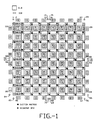
- Circuit intégré comprenant une matrice logique configurable, comprenant:- une pluralité de zones logiques (500) définies sur le circuit intégré, chaque zone logique ayant un périmètre et des circuits logiques programmables disposés à l'intérieur du périmètre pour exécuter des opérations logiques dans ceux-ci selon des données de configuration fournies par un utilisateur;- dans lequel chaque zone logique est divisible symétriquement en au moins quatre parties de zone logique;- dans lequel chaque zone logique comporte cinq bornes d'entrée ou plus (A1 à A4, B1 à B4, C1 à C4, D1 à D4, EM1 à EM4, EN1 à EN4, FM1 à FM4, FN1 à FN4, G1 à G4, H1 à H4) disposées d'une manière répartie le long du périmètre de la zone logique pour recevoir cinq signaux d'entrée ou plus fournis de l'extérieur du périmètre et pour conduire les cinq signaux d'entrée ou plus fournis de l'extérieur dans la zone logique;- dans lequel les circuits logiques programmables de chaque zone logique comprennent des moyens de logique combinatoire (701.1 à 8, 702.1 à 4, 704.1 à 2, 705, 706) connectés fonctionnellement aux cinq bornes d'entrée ou plus de la zone logique pour produire une pluralité de signaux de logique combinatoire (FC1 à FC4, FD1 à FD4, FE1 et FE2, F et H);- dans lequel chaque zone logique comprend en outre au moins quatre macrocellules de sortie (figures 21 à 25) connectées fonctionnellement aux moyens de logique combinatoire correspondants (701.1 à 8, 702.1 à 4, 704.1 à 2, 705, 706) de la zone logique et disposées pour fournir d'une manière répartie les signaux de logique combinatoire (FC1 à FC4, FD1 à FD4, FE1 et FE2, F, H) produits par les moyens de logique combinatoire correspondants de la zone logique respectivement issus des quatre parties de la zone logique;- dans lequel chacune des quatre macrocellules de sortie comprend un moyen de sortie (X1, Y1, X2, Y2, X3, Y3, X4, Y4) pour fournir au moins un signal logique (FC1 à FC4, FD1 à FD4, FE1 à FE2, F, H) à partir de la partie respective de zone logique correspondant à cette macrocellule; et- dans lequel lesdites macrocellules sont connectées auxdits moyens de logique combinatoire de telle manière qu'au moins un (H) des signaux de logique combinatoire (FC1 à FC4, D1 à D4, FE1 et FE2, F, H) produits par les moyens de logique combinatoire de chaque zone logique soit une fonction d'au moins cinq des signaux d'entrée fournis de l'extérieur (A1 à A4, B1 à B4, C1 à C4, D1 à D4, EM1 à EM4, EN1 à EN4, FM1 à FM4, FN1 à FN4, G1 à G4, H1 à H4) de la zone logique correspondante;ce par quoi chacune des quatre macrocellules de sortie de chaque zone logique est agencée de telle manière que ses moyens de sortie peuvent fournir le même dit au moins un signal (H) en tant que signal non mis en registre à partir de l'une quelconque des quatre parties respectives de zone logique de la zone logique correspondante.
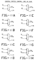
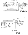
- Circuit intégré selon la revendication 1, dans lequel chaque zone logique (500) comprend au moins un registre mémorisant un signal (202) et chacune des quatre macrocellules de sortie comprend en outre des moyens de sortie (X1, Y1, X2, Y2, X3, Y3, X4, Y4) pour registre dudit au moins un signal logique (H) à partir de la zone respective parmi les quatre zones logiques (500) correspondant à cette macrocellule, ladite version en registre du au moins un signal logique (H) étant fournie à partir du au moins un registre mémorisant un signal (202) de la zone logique.
- Circuit intégré selon la revendication 2, dans lequel chaque zone logique (500) comprend quatre registres mémorisant un signal, un pour chacune des quatre macrocellules de sortie, et chacun étant connecté pour recevoir le au moins signal logique (H) issu des moyens logiques correspondants de la zone logique (500); et- dans lequel les moyens de sortie (X1, Y1, X2, Y2, X3, Y3, X4, Y4) de chacune des quatre macrocellules de sortie reçoivent une version en registre dudit au moins un signal logique (H) issue d'un registre respectif parmi les quatre registre mémorisant un signal.
- Circuit intégré selon la revendication 1, comprenant en outre un réseau d'interconnexion configurable défini sur le circuit intégré, dans lequel les zones logiques (500) de la pluralité de zone logiques sont espacées les unes des autres et interconnectées par le réseau d'interconnexion configurable.
- Circuit intégré selon la revendication 4, dans lequel quatre ou plus des bornes d'entrée (A1 à A4, B1 à B4, C1 à C4, D1 à D4, EM1 à EM4, EN1 à EN4, FM1 à FM4, FN1 à FN4, G1 à G4, H1 à H4) dans chaque zone logique (500) sont réparties symétriquement le long du périmètre de la zone logique (500) et le réseau d'interconnexion configurable comprend des ensembles correspondants de bus d'interconnexion disposés symétriquement autour de chaque zone logique (500) pour fournir des signaux d'entrée aux bornes d'entrée (A1 à A4, B1 à B4, C1 à C4, D1 à D4, EM1 à EM4, EN1 à EN4, FM1 à FM4, FN1 à FN4, G1 à G4, H1 à H4) des zones logiques (500).
- Circuit intégré selon la revendication 1, dans lequel quatre ou plus des bornes d'entrée (A1 à A4, B1 à B4, C1 à C4, D1 à D4, EM1 à EM4, EN1 à EN4, FM1 à FM4, FN1 à FN4, G1 à G4, H1 à H4) dans chaque zone logique (500) sont réparties symétriquement le long du périmètre de la zone logique (500).
- Circuit intégré selon la revendication 1, dans lequel il y a seize bornes d'entrée (A1 à A4, B1 à B4, C1 à C4, D1 à D4, EM1 à EM4, EN1 à EN4, FM1 à FM4, FN1 à FN4, G1 à G4, H1 à H4) disposées de manière répartie le long du périmètre de chaque zone logique (500) pour recevoir seize signaux d'entrée fournis de l'extérieur du périmètre et pour conduire les seize signaux d'entrée fournis de l'extérieur dans la zone logique (500); et- ledit au moins signal logique (H) parmi les signaux d'entrée combinatoires de chaque zone logique (500) est une fonction des seize signaux d'entrée fournis de l'extérieur.
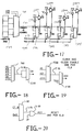
- Circuit intégré selon la revendication 1, comprenant en outre un réseau d'interconnexion configurable défini sur le circuit intégré, le réseau d'interconnexion comprenant au moins quatre lignes à trois états passant près des au moins quatre parties de zone logique de chacune des zones logiques (500); et- dans lequel chacune des quatre macrocellules de sortie de chaque zone logique (500) comporte un circuit tampon à trois états pour fournir les signaux de logique combinatoire (FC1 à FC4, D1 à D4, FE1 et FE2, F, H) produits par les moyens de logique combinatoire correspondants (701.1 à 8, 702.1 à 4, 704.1 et 2, 705, 706), à l'extérieur de la zone logique (500) et à une ligne à trois états correspondante voisine de sa partie correspondante de zone logique.
Applications Claiming Priority (2)
| Application Number | Priority Date | Filing Date | Title |
|---|---|---|---|
| US07/514,297 US5231588A (en) | 1989-08-15 | 1990-04-25 | Programmable gate array with logic cells having symmetrical input/output structures |
| US514297 | 1990-04-25 |
Publications (2)
| Publication Number | Publication Date |
|---|---|
| EP0454352A1 EP0454352A1 (fr) | 1991-10-30 |
| EP0454352B1 true EP0454352B1 (fr) | 1997-03-19 |
Family
ID=24046601
Family Applications (1)
| Application Number | Title | Priority Date | Filing Date |
|---|---|---|---|
| EP91303446A Expired - Lifetime EP0454352B1 (fr) | 1990-04-25 | 1991-04-18 | Matrice logique configurable |
Country Status (5)
| Country | Link |
|---|---|
| US (1) | US5231588A (fr) |
| EP (1) | EP0454352B1 (fr) |
| JP (1) | JPH06112444A (fr) |
| AT (1) | ATE150600T1 (fr) |
| DE (1) | DE69125201T2 (fr) |
Families Citing this family (80)
| Publication number | Priority date | Publication date | Assignee | Title |
|---|---|---|---|---|
| US5451887A (en) * | 1986-09-19 | 1995-09-19 | Actel Corporation | Programmable logic module and architecture for field programmable gate array device |
| US5477165A (en) * | 1986-09-19 | 1995-12-19 | Actel Corporation | Programmable logic module and architecture for field programmable gate array device |
| US5367208A (en) | 1986-09-19 | 1994-11-22 | Actel Corporation | Reconfigurable programmable interconnect architecture |
| US5644497A (en) * | 1988-03-15 | 1997-07-01 | Hyman; Edward | Method and apparatus for compiling and implementing state-machine states and outputs for a universal cellular sequential logic array |
| US5377123A (en) * | 1992-06-08 | 1994-12-27 | Hyman; Edward | Programmable logic device |
| US5452231A (en) * | 1988-10-05 | 1995-09-19 | Quickturn Design Systems, Inc. | Hierarchically connected reconfigurable logic assembly |
| US5343406A (en) * | 1989-07-28 | 1994-08-30 | Xilinx, Inc. | Distributed memory architecture for a configurable logic array and method for using distributed memory |
| US5377124A (en) * | 1989-09-20 | 1994-12-27 | Aptix Corporation | Field programmable printed circuit board |
| US5198705A (en) * | 1990-05-11 | 1993-03-30 | Actel Corporation | Logic module with configurable combinational and sequential blocks |
| DE69133311T2 (de) * | 1990-10-15 | 2004-06-24 | Aptix Corp., San Jose | Verbindungssubstrat mit integrierter Schaltung zur programmierbaren Verbindung und Probenuntersuchung |
| JP2854733B2 (ja) * | 1991-08-23 | 1999-02-03 | 三菱電機株式会社 | 遅延時間計算装置及び遅延時間計算方法 |
| US5432708A (en) * | 1992-10-08 | 1995-07-11 | Aptix Corporation | Multichip module integrated circuit device having maximum input/output capability |
| US5414638A (en) * | 1992-12-18 | 1995-05-09 | Aptix Corporation | Programmable interconnect architecture |
| US5381058A (en) * | 1993-05-21 | 1995-01-10 | At&T Corp. | FPGA having PFU with programmable output driver inputs |
| US5438295A (en) * | 1993-06-11 | 1995-08-01 | Altera Corporation | Look-up table using multi-level decode |
| US5815024A (en) * | 1993-06-11 | 1998-09-29 | Altera Corporation | Look-up table using multi-level decode |
| US5457410A (en) * | 1993-08-03 | 1995-10-10 | Btr, Inc. | Architecture and interconnect scheme for programmable logic circuits |
| US5457644A (en) * | 1993-08-20 | 1995-10-10 | Actel Corporation | Field programmable digital signal processing array integrated circuit |
| US5680583A (en) | 1994-02-16 | 1997-10-21 | Arkos Design, Inc. | Method and apparatus for a trace buffer in an emulation system |
| US5550843A (en) * | 1994-04-01 | 1996-08-27 | Xilinx, Inc. | Programmable scan chain testing structure and method |
| US5909126A (en) * | 1995-05-17 | 1999-06-01 | Altera Corporation | Programmable logic array integrated circuit devices with interleaved logic array blocks |
| US5625301A (en) * | 1995-05-18 | 1997-04-29 | Actel Corporation | Flexible FPGA input/output architecture |
| US5646546A (en) * | 1995-06-02 | 1997-07-08 | International Business Machines Corporation | Programmable logic cell having configurable gates and multiplexers |
| US5671432A (en) * | 1995-06-02 | 1997-09-23 | International Business Machines Corporation | Programmable array I/O-routing resource |
| US5631578A (en) * | 1995-06-02 | 1997-05-20 | International Business Machines Corporation | Programmable array interconnect network |
| US5848285A (en) * | 1995-12-26 | 1998-12-08 | Cypress Semiconductor Corporation | Macrocell having a dual purpose input register for use in a logic device |
| US5760719A (en) * | 1995-12-29 | 1998-06-02 | Cypress Semiconductor Corp. | Programmable I/O cell with data conversion capability |
| US5811989A (en) * | 1995-12-29 | 1998-09-22 | Cypress Semiconductor Corp. | Programmable I/O cell with data conversion capability |
| US5786710A (en) * | 1995-12-29 | 1998-07-28 | Cypress Semiconductor Corp. | Programmable I/O cell with data conversion capability |
| US5917337A (en) * | 1995-12-29 | 1999-06-29 | Cypress Semiconductor Corp. | Programmable I/O cell with data conversion capability |
| US5847580A (en) * | 1996-10-10 | 1998-12-08 | Xilinx, Inc. | High speed bidirectional bus with multiplexers |
| US5936424A (en) * | 1996-02-02 | 1999-08-10 | Xilinx, Inc. | High speed bus with tree structure for selecting bus driver |
| US5808897A (en) * | 1996-03-05 | 1998-09-15 | Micron Technology, Inc. | Integrated circuit device having interchangeable terminal connection |
| US6034540A (en) * | 1997-04-08 | 2000-03-07 | Altera Corporation | Programmable logic integrated circuit architecture incorporating a lonely register |
| US5986465A (en) * | 1996-04-09 | 1999-11-16 | Altera Corporation | Programmable logic integrated circuit architecture incorporating a global shareable expander |
| US5894565A (en) * | 1996-05-20 | 1999-04-13 | Atmel Corporation | Field programmable gate array with distributed RAM and increased cell utilization |
| US6624658B2 (en) * | 1999-02-04 | 2003-09-23 | Advantage Logic, Inc. | Method and apparatus for universal program controlled bus architecture |
| US6034547A (en) | 1996-09-04 | 2000-03-07 | Advantage Logic, Inc. | Method and apparatus for universal program controlled bus |
| US5781032A (en) * | 1996-09-09 | 1998-07-14 | International Business Machines Corporation | Programmable inverter circuit used in a programmable logic cell |
| US5841967A (en) | 1996-10-17 | 1998-11-24 | Quickturn Design Systems, Inc. | Method and apparatus for design verification using emulation and simulation |
| US5959466A (en) | 1997-01-31 | 1999-09-28 | Actel Corporation | Field programmable gate array with mask programmed input and output buffers |
| US5936426A (en) | 1997-02-03 | 1999-08-10 | Actel Corporation | Logic function module for field programmable array |
| US5999015A (en) * | 1997-02-20 | 1999-12-07 | Altera Corporation | Logic region resources for programmable logic devices |
| US5982195A (en) * | 1997-02-20 | 1999-11-09 | Altera Corporation | Programmable logic device architectures |
| US5920202A (en) * | 1997-02-26 | 1999-07-06 | Xilinx, Inc. | Configurable logic element with ability to evaluate five and six input functions |
| US5889411A (en) * | 1997-02-26 | 1999-03-30 | Xilinx, Inc. | FPGA having logic element carry chains capable of generating wide XOR functions |
| US5963050A (en) | 1997-02-26 | 1999-10-05 | Xilinx, Inc. | Configurable logic element with fast feedback paths |
| US5914616A (en) * | 1997-02-26 | 1999-06-22 | Xilinx, Inc. | FPGA repeatable interconnect structure with hierarchical interconnect lines |
| US6201410B1 (en) | 1997-02-26 | 2001-03-13 | Xilinx, Inc. | Wide logic gate implemented in an FPGA configurable logic element |
| US5942913A (en) * | 1997-03-20 | 1999-08-24 | Xilinx, Inc. | FPGA repeatable interconnect structure with bidirectional and unidirectional interconnect lines |
| US6204689B1 (en) | 1997-02-26 | 2001-03-20 | Xilinx, Inc. | Input/output interconnect circuit for FPGAs |
| US6150837A (en) * | 1997-02-28 | 2000-11-21 | Actel Corporation | Enhanced field programmable gate array |
| US6389379B1 (en) | 1997-05-02 | 2002-05-14 | Axis Systems, Inc. | Converification system and method |
| US6026230A (en) * | 1997-05-02 | 2000-02-15 | Axis Systems, Inc. | Memory simulation system and method |
| US6421251B1 (en) | 1997-05-02 | 2002-07-16 | Axis Systems Inc | Array board interconnect system and method |
| US6321366B1 (en) | 1997-05-02 | 2001-11-20 | Axis Systems, Inc. | Timing-insensitive glitch-free logic system and method |
| US6009256A (en) * | 1997-05-02 | 1999-12-28 | Axis Systems, Inc. | Simulation/emulation system and method |
| US6134516A (en) * | 1997-05-02 | 2000-10-17 | Axis Systems, Inc. | Simulation server system and method |
| US5960191A (en) | 1997-05-30 | 1999-09-28 | Quickturn Design Systems, Inc. | Emulation system with time-multiplexed interconnect |
| US6006321A (en) * | 1997-06-13 | 1999-12-21 | Malleable Technologies, Inc. | Programmable logic datapath that may be used in a field programmable device |
| US6150836A (en) * | 1997-06-13 | 2000-11-21 | Malleable Technologies, Inc. | Multilevel logic field programmable device |
| US5970240A (en) | 1997-06-25 | 1999-10-19 | Quickturn Design Systems, Inc. | Method and apparatus for configurable memory emulation |
| US5974435A (en) * | 1997-08-28 | 1999-10-26 | Malleable Technologies, Inc. | Reconfigurable arithmetic datapath |
| US6084427A (en) | 1998-05-19 | 2000-07-04 | Altera Corporation | Programmable logic devices with enhanced multiplexing capabilities |
| US6121790A (en) * | 1997-10-16 | 2000-09-19 | Altera Corporation | Programmable logic device with enhanced multiplexing capabilities in interconnect resources |
| US6215326B1 (en) | 1998-11-18 | 2001-04-10 | Altera Corporation | Programmable logic device architecture with super-regions having logic regions and a memory region |
| US6407576B1 (en) | 1999-03-04 | 2002-06-18 | Altera Corporation | Interconnection and input/output resources for programmable logic integrated circuit devices |
| WO2000068775A1 (fr) * | 1999-05-07 | 2000-11-16 | Morphics Technology Inc. | Appareil et procede pour circuits arithmetiques de trajet de donnees programmables |
| US6438569B1 (en) | 1999-09-20 | 2002-08-20 | Pmc-Sierra, Inc. | Sums of production datapath |
| JP3472527B2 (ja) | 2000-05-16 | 2003-12-02 | 松下電器産業株式会社 | 論理回路モジュール及びこれを用いた半導体集積回路の設計方法並びに半導体集積回路 |
| EP1233517B1 (fr) * | 2001-02-09 | 2012-04-18 | Sicronic Remote KG, LLC | Système de configuration rapide d'un dispositif logique programmable |
| US7255437B2 (en) * | 2003-10-09 | 2007-08-14 | Howell Thomas A | Eyeglasses with activity monitoring |
| US7796464B1 (en) | 2003-06-27 | 2010-09-14 | Cypress Semiconductor Corporation | Synchronous memory with a shadow-cycle counter |
| US7893772B1 (en) | 2007-12-03 | 2011-02-22 | Cypress Semiconductor Corporation | System and method of loading a programmable counter |
| US8438522B1 (en) | 2008-09-24 | 2013-05-07 | Iowa State University Research Foundation, Inc. | Logic element architecture for generic logic chains in programmable devices |
| US8661394B1 (en) | 2008-09-24 | 2014-02-25 | Iowa State University Research Foundation, Inc. | Depth-optimal mapping of logic chains in reconfigurable fabrics |
| US8868820B2 (en) * | 2011-10-31 | 2014-10-21 | Microsemi SoC Corporation | RAM block designed for efficient ganging |
| US8959010B1 (en) | 2011-12-08 | 2015-02-17 | Cadence Design Systems, Inc. | Emulation system with improved reliability of interconnect and a method for programming such interconnect |
| US8743735B1 (en) | 2012-01-18 | 2014-06-03 | Cadence Design Systems, Inc. | Emulation system for verifying a network device |
| US8595683B1 (en) | 2012-04-12 | 2013-11-26 | Cadence Design Systems, Inc. | Generating user clocks for a prototyping environment |
Family Cites Families (9)
| Publication number | Priority date | Publication date | Assignee | Title |
|---|---|---|---|---|
| US4870302A (en) * | 1984-03-12 | 1989-09-26 | Xilinx, Inc. | Configurable electrical circuit having configurable logic elements and configurable interconnects |
| US4688072A (en) * | 1984-06-29 | 1987-08-18 | Hughes Aircraft Company | Hierarchical configurable gate array |
| US4713557A (en) * | 1984-09-26 | 1987-12-15 | Xilinx, Inc. | Bidirectional buffer amplifier |
| US4642487A (en) * | 1984-09-26 | 1987-02-10 | Xilinx, Inc. | Special interconnect for configurable logic array |
| US4706216A (en) * | 1985-02-27 | 1987-11-10 | Xilinx, Inc. | Configurable logic element |
| KR900008022B1 (ko) * | 1986-10-16 | 1990-10-29 | 페어차일드 세미콘덕터 코퍼레이션 | 동기배열논리회로 및 시스템 |
| EP0651343B1 (fr) * | 1988-10-05 | 2004-04-28 | Quickturn Design Systems, Inc. | Procédé pour utiliser des puces logiques de circuits prédiffusés reconfigurables électroniquement et appareil ainsi formé |
| US5203005A (en) * | 1989-05-02 | 1993-04-13 | Horst Robert W | Cell structure for linear array wafer scale integration architecture with capability to open boundary i/o bus without neighbor acknowledgement |
| US5212652A (en) * | 1989-08-15 | 1993-05-18 | Advanced Micro Devices, Inc. | Programmable gate array with improved interconnect structure |
-
1990
- 1990-04-25 US US07/514,297 patent/US5231588A/en not_active Expired - Fee Related
-
1991
- 1991-04-18 DE DE69125201T patent/DE69125201T2/de not_active Expired - Fee Related
- 1991-04-18 AT AT91303446T patent/ATE150600T1/de not_active IP Right Cessation
- 1991-04-18 EP EP91303446A patent/EP0454352B1/fr not_active Expired - Lifetime
- 1991-04-25 JP JP3094521A patent/JPH06112444A/ja not_active Withdrawn
Also Published As
| Publication number | Publication date |
|---|---|
| DE69125201D1 (de) | 1997-04-24 |
| DE69125201T2 (de) | 1997-10-09 |
| US5231588A (en) | 1993-07-27 |
| JPH06112444A (ja) | 1994-04-22 |
| EP0454352A1 (fr) | 1991-10-30 |
| ATE150600T1 (de) | 1997-04-15 |
Similar Documents
| Publication | Publication Date | Title |
|---|---|---|
| EP0454352B1 (fr) | Matrice logique configurable | |
| US5185706A (en) | Programmable gate array with logic cells having configurable output enable | |
| US5740069A (en) | Logic device (PLD) having direct connections between configurable logic blocks (CLBs) and configurable input/output blocks (IOBs) | |
| US5260881A (en) | Programmable gate array with improved configurable logic block | |
| US5233539A (en) | Programmable gate array with improved interconnect structure, input/output structure and configurable logic block | |
| US4963768A (en) | Flexible, programmable cell array interconnected by a programmable switch matrix | |
| US6028808A (en) | Programmable logic array integrated circuits | |
| EP0461798B1 (fr) | Structure d'interconnexion configurable | |
| US5828229A (en) | Programmable logic array integrated circuits | |
| EP0746102B1 (fr) | Circuit intégré de réseaux logiques programmables | |
| JPH07504797A (ja) | 論理積項の縦続接続および改良したフリップフロップ利用を伴うマクロセル | |
| US5883850A (en) | Programmable logic array integrated circuits | |
| US6897679B2 (en) | Programmable logic array integrated circuits | |
| US6462576B1 (en) | Programmable logic device |
Legal Events
| Date | Code | Title | Description |
|---|---|---|---|
| PUAI | Public reference made under article 153(3) epc to a published international application that has entered the european phase |
Free format text: ORIGINAL CODE: 0009012 |
|
| AK | Designated contracting states |
Kind code of ref document: A1 Designated state(s): AT BE CH DE DK ES FR GB GR IT LI LU NL SE |
|
| 17P | Request for examination filed |
Effective date: 19920402 |
|
| 17Q | First examination report despatched |
Effective date: 19941028 |
|
| GRAG | Despatch of communication of intention to grant |
Free format text: ORIGINAL CODE: EPIDOS AGRA |
|
| GRAH | Despatch of communication of intention to grant a patent |
Free format text: ORIGINAL CODE: EPIDOS IGRA |
|
| GRAH | Despatch of communication of intention to grant a patent |
Free format text: ORIGINAL CODE: EPIDOS IGRA |
|
| GRAA | (expected) grant |
Free format text: ORIGINAL CODE: 0009210 |
|
| AK | Designated contracting states |
Kind code of ref document: B1 Designated state(s): AT BE CH DE DK ES FR GB GR IT LI LU NL SE |
|
| PG25 | Lapsed in a contracting state [announced via postgrant information from national office to epo] |
Ref country code: IT Free format text: LAPSE BECAUSE OF FAILURE TO SUBMIT A TRANSLATION OF THE DESCRIPTION OR TO PAY THE FEE WITHIN THE PRE;WARNING: LAPSES OF ITALIAN PATENTS WITH EFFECTIVE DATE BEFORE 2007 MAY HAVE OCCURRED AT ANY TIME BEFORE 2007. THE CORRECT EFFECTIVE DATE MAY BE DIFFERENT FROM THE ONE RECORDED.SCRIBED TIME-LIMIT Effective date: 19970319 Ref country code: CH Effective date: 19970319 Ref country code: LI Effective date: 19970319 Ref country code: ES Free format text: THE PATENT HAS BEEN ANNULLED BY A DECISION OF A NATIONAL AUTHORITY Effective date: 19970319 Ref country code: GR Free format text: LAPSE BECAUSE OF FAILURE TO SUBMIT A TRANSLATION OF THE DESCRIPTION OR TO PAY THE FEE WITHIN THE PRESCRIBED TIME-LIMIT Effective date: 19970319 Ref country code: AT Effective date: 19970319 Ref country code: BE Effective date: 19970319 Ref country code: DK Effective date: 19970319 Ref country code: NL Free format text: LAPSE BECAUSE OF FAILURE TO SUBMIT A TRANSLATION OF THE DESCRIPTION OR TO PAY THE FEE WITHIN THE PRESCRIBED TIME-LIMIT Effective date: 19970319 |
|
| REF | Corresponds to: |
Ref document number: 150600 Country of ref document: AT Date of ref document: 19970415 Kind code of ref document: T |
|
| REG | Reference to a national code |
Ref country code: CH Ref legal event code: EP |
|
| PG25 | Lapsed in a contracting state [announced via postgrant information from national office to epo] |
Ref country code: LU Free format text: LAPSE BECAUSE OF NON-PAYMENT OF DUE FEES Effective date: 19970418 |
|
| REF | Corresponds to: |
Ref document number: 69125201 Country of ref document: DE Date of ref document: 19970424 |
|
| PG25 | Lapsed in a contracting state [announced via postgrant information from national office to epo] |
Ref country code: SE Effective date: 19970619 |
|
| ET | Fr: translation filed | ||
| NLV1 | Nl: lapsed or annulled due to failure to fulfill the requirements of art. 29p and 29m of the patents act | ||
| REG | Reference to a national code |
Ref country code: CH Ref legal event code: PL |
|
| PLBE | No opposition filed within time limit |
Free format text: ORIGINAL CODE: 0009261 |
|
| STAA | Information on the status of an ep patent application or granted ep patent |
Free format text: STATUS: NO OPPOSITION FILED WITHIN TIME LIMIT |
|
| 26N | No opposition filed | ||
| PGFP | Annual fee paid to national office [announced via postgrant information from national office to epo] |
Ref country code: FR Payment date: 20010405 Year of fee payment: 11 |
|
| PGFP | Annual fee paid to national office [announced via postgrant information from national office to epo] |
Ref country code: DE Payment date: 20010430 Year of fee payment: 11 |
|
| REG | Reference to a national code |
Ref country code: GB Ref legal event code: IF02 |
|
| PG25 | Lapsed in a contracting state [announced via postgrant information from national office to epo] |
Ref country code: DE Free format text: LAPSE BECAUSE OF NON-PAYMENT OF DUE FEES Effective date: 20021101 |
|
| PG25 | Lapsed in a contracting state [announced via postgrant information from national office to epo] |
Ref country code: FR Free format text: LAPSE BECAUSE OF NON-PAYMENT OF DUE FEES Effective date: 20021231 |
|
| REG | Reference to a national code |
Ref country code: GB Ref legal event code: 732E |
|
| REG | Reference to a national code |
Ref country code: FR Ref legal event code: ST |
|
| PGFP | Annual fee paid to national office [announced via postgrant information from national office to epo] |
Ref country code: GB Payment date: 20040414 Year of fee payment: 14 |
|
| PG25 | Lapsed in a contracting state [announced via postgrant information from national office to epo] |
Ref country code: GB Free format text: LAPSE BECAUSE OF NON-PAYMENT OF DUE FEES Effective date: 20050418 |
|
| GBPC | Gb: european patent ceased through non-payment of renewal fee |
Effective date: 20050418 |