EP0451939A2 - Recording apparatus with a recording head having a wiring substrate - Google Patents
Recording apparatus with a recording head having a wiring substrate Download PDFInfo
- Publication number
- EP0451939A2 EP0451939A2 EP91301490A EP91301490A EP0451939A2 EP 0451939 A2 EP0451939 A2 EP 0451939A2 EP 91301490 A EP91301490 A EP 91301490A EP 91301490 A EP91301490 A EP 91301490A EP 0451939 A2 EP0451939 A2 EP 0451939A2
- Authority
- EP
- European Patent Office
- Prior art keywords
- layer
- protective layer
- electroconductive
- layers
- protective
- Prior art date
- Legal status (The legal status is an assumption and is not a legal conclusion. Google has not performed a legal analysis and makes no representation as to the accuracy of the status listed.)
- Granted
Links
- 239000000758 substrate Substances 0.000 title claims abstract description 86
- 239000010410 layer Substances 0.000 claims abstract description 222
- 239000011241 protective layer Substances 0.000 claims abstract description 104
- 239000007788 liquid Substances 0.000 claims abstract description 36
- 238000007599 discharging Methods 0.000 claims description 17
- 239000011229 interlayer Substances 0.000 claims description 11
- 239000011368 organic material Substances 0.000 claims description 11
- 239000004065 semiconductor Substances 0.000 claims description 10
- 229910010272 inorganic material Inorganic materials 0.000 claims description 5
- 239000011147 inorganic material Substances 0.000 claims description 5
- 239000004020 conductor Substances 0.000 claims 2
- 238000009429 electrical wiring Methods 0.000 claims 2
- 230000015572 biosynthetic process Effects 0.000 abstract description 4
- 239000007921 spray Substances 0.000 abstract description 3
- VYPSYNLAJGMNEJ-UHFFFAOYSA-N Silicium dioxide Chemical compound O=[Si]=O VYPSYNLAJGMNEJ-UHFFFAOYSA-N 0.000 description 34
- 239000010408 film Substances 0.000 description 31
- 238000005530 etching Methods 0.000 description 23
- 229920002120 photoresistant polymer Polymers 0.000 description 22
- 238000004544 sputter deposition Methods 0.000 description 20
- 238000000576 coating method Methods 0.000 description 19
- 239000000463 material Substances 0.000 description 18
- 229910052681 coesite Inorganic materials 0.000 description 17
- 229910052906 cristobalite Inorganic materials 0.000 description 17
- 239000000377 silicon dioxide Substances 0.000 description 17
- 235000012239 silicon dioxide Nutrition 0.000 description 17
- 229910052682 stishovite Inorganic materials 0.000 description 17
- 229910052905 tridymite Inorganic materials 0.000 description 17
- 229920001721 polyimide Polymers 0.000 description 16
- 239000004642 Polyimide Substances 0.000 description 15
- 229910000679 solder Inorganic materials 0.000 description 15
- 239000011248 coating agent Substances 0.000 description 13
- 229910052751 metal Inorganic materials 0.000 description 12
- 239000002184 metal Substances 0.000 description 12
- 238000010276 construction Methods 0.000 description 11
- 239000007789 gas Substances 0.000 description 11
- 238000000034 method Methods 0.000 description 10
- 238000000059 patterning Methods 0.000 description 9
- 229910003862 HfB2 Inorganic materials 0.000 description 7
- 230000004888 barrier function Effects 0.000 description 7
- 238000004519 manufacturing process Methods 0.000 description 7
- QTBSBXVTEAMEQO-UHFFFAOYSA-N Acetic acid Chemical compound CC(O)=O QTBSBXVTEAMEQO-UHFFFAOYSA-N 0.000 description 6
- 238000007796 conventional method Methods 0.000 description 6
- 238000010438 heat treatment Methods 0.000 description 6
- 230000003064 anti-oxidating effect Effects 0.000 description 5
- 230000007423 decrease Effects 0.000 description 5
- 238000003475 lamination Methods 0.000 description 5
- XKRFYHLGVUSROY-UHFFFAOYSA-N Argon Chemical compound [Ar] XKRFYHLGVUSROY-UHFFFAOYSA-N 0.000 description 4
- NBIIXXVUZAFLBC-UHFFFAOYSA-N Phosphoric acid Chemical compound OP(O)(O)=O NBIIXXVUZAFLBC-UHFFFAOYSA-N 0.000 description 4
- RKTYLMNFRDHKIL-UHFFFAOYSA-N copper;5,10,15,20-tetraphenylporphyrin-22,24-diide Chemical compound [Cu+2].C1=CC(C(=C2C=CC([N-]2)=C(C=2C=CC=CC=2)C=2C=CC(N=2)=C(C=2C=CC=CC=2)C2=CC=C3[N-]2)C=2C=CC=CC=2)=NC1=C3C1=CC=CC=C1 RKTYLMNFRDHKIL-UHFFFAOYSA-N 0.000 description 4
- 239000010409 thin film Substances 0.000 description 4
- 238000009835 boiling Methods 0.000 description 3
- 238000003486 chemical etching Methods 0.000 description 3
- 238000011161 development Methods 0.000 description 3
- 230000000694 effects Effects 0.000 description 3
- 238000001459 lithography Methods 0.000 description 3
- KRHYYFGTRYWZRS-UHFFFAOYSA-N Fluorane Chemical compound F KRHYYFGTRYWZRS-UHFFFAOYSA-N 0.000 description 2
- GRYLNZFGIOXLOG-UHFFFAOYSA-N Nitric acid Chemical compound O[N+]([O-])=O GRYLNZFGIOXLOG-UHFFFAOYSA-N 0.000 description 2
- 229910000147 aluminium phosphate Inorganic materials 0.000 description 2
- ROOXNKNUYICQNP-UHFFFAOYSA-N ammonium persulfate Chemical compound [NH4+].[NH4+].[O-]S(=O)(=O)OOS([O-])(=O)=O ROOXNKNUYICQNP-UHFFFAOYSA-N 0.000 description 2
- 229910052786 argon Inorganic materials 0.000 description 2
- 229910052802 copper Inorganic materials 0.000 description 2
- 239000013078 crystal Substances 0.000 description 2
- 230000007547 defect Effects 0.000 description 2
- 238000000151 deposition Methods 0.000 description 2
- 230000008021 deposition Effects 0.000 description 2
- 239000003822 epoxy resin Substances 0.000 description 2
- 239000011521 glass Substances 0.000 description 2
- 239000000203 mixture Substances 0.000 description 2
- 238000012986 modification Methods 0.000 description 2
- 230000004048 modification Effects 0.000 description 2
- 229910017604 nitric acid Inorganic materials 0.000 description 2
- 229920000647 polyepoxide Polymers 0.000 description 2
- 239000011347 resin Substances 0.000 description 2
- 229920005989 resin Polymers 0.000 description 2
- 239000004925 Acrylic resin Substances 0.000 description 1
- 229920000178 Acrylic resin Polymers 0.000 description 1
- 229910017083 AlN Inorganic materials 0.000 description 1
- 229910001020 Au alloy Inorganic materials 0.000 description 1
- 229910015844 BCl3 Inorganic materials 0.000 description 1
- XPDWGBQVDMORPB-UHFFFAOYSA-N Fluoroform Chemical compound FC(F)F XPDWGBQVDMORPB-UHFFFAOYSA-N 0.000 description 1
- 229910004541 SiN Inorganic materials 0.000 description 1
- 239000000853 adhesive Substances 0.000 description 1
- 230000001070 adhesive effect Effects 0.000 description 1
- PNEYBMLMFCGWSK-UHFFFAOYSA-N aluminium oxide Inorganic materials [O-2].[O-2].[O-2].[Al+3].[Al+3] PNEYBMLMFCGWSK-UHFFFAOYSA-N 0.000 description 1
- 229910001870 ammonium persulfate Inorganic materials 0.000 description 1
- 230000005540 biological transmission Effects 0.000 description 1
- 230000008859 change Effects 0.000 description 1
- 238000005229 chemical vapour deposition Methods 0.000 description 1
- 229910052804 chromium Inorganic materials 0.000 description 1
- 238000004140 cleaning Methods 0.000 description 1
- 230000007797 corrosion Effects 0.000 description 1
- 238000005260 corrosion Methods 0.000 description 1
- 229910052593 corundum Inorganic materials 0.000 description 1
- 238000013461 design Methods 0.000 description 1
- 238000007598 dipping method Methods 0.000 description 1
- 230000008020 evaporation Effects 0.000 description 1
- 238000001704 evaporation Methods 0.000 description 1
- 230000002349 favourable effect Effects 0.000 description 1
- 229910052737 gold Inorganic materials 0.000 description 1
- 230000006872 improvement Effects 0.000 description 1
- 238000009413 insulation Methods 0.000 description 1
- 239000012212 insulator Substances 0.000 description 1
- 238000011835 investigation Methods 0.000 description 1
- 239000011344 liquid material Substances 0.000 description 1
- 230000007774 longterm Effects 0.000 description 1
- 150000002739 metals Chemical class 0.000 description 1
- 229910003465 moissanite Inorganic materials 0.000 description 1
- 229910052759 nickel Inorganic materials 0.000 description 1
- 230000006911 nucleation Effects 0.000 description 1
- 238000010899 nucleation Methods 0.000 description 1
- 239000002674 ointment Substances 0.000 description 1
- 230000003647 oxidation Effects 0.000 description 1
- 238000007254 oxidation reaction Methods 0.000 description 1
- 238000007747 plating Methods 0.000 description 1
- 239000009719 polyimide resin Substances 0.000 description 1
- 238000003825 pressing Methods 0.000 description 1
- 238000007639 printing Methods 0.000 description 1
- 230000002035 prolonged effect Effects 0.000 description 1
- 230000001681 protective effect Effects 0.000 description 1
- 238000011084 recovery Methods 0.000 description 1
- 230000009467 reduction Effects 0.000 description 1
- 230000004044 response Effects 0.000 description 1
- 230000000717 retained effect Effects 0.000 description 1
- 230000002441 reversible effect Effects 0.000 description 1
- 238000007650 screen-printing Methods 0.000 description 1
- 238000004904 shortening Methods 0.000 description 1
- 229910052710 silicon Inorganic materials 0.000 description 1
- 239000010703 silicon Substances 0.000 description 1
- 229910010271 silicon carbide Inorganic materials 0.000 description 1
- 229920002050 silicone resin Polymers 0.000 description 1
- 239000002356 single layer Substances 0.000 description 1
- 239000007787 solid Substances 0.000 description 1
- 239000011343 solid material Substances 0.000 description 1
- 238000004528 spin coating Methods 0.000 description 1
- PBCFLUZVCVVTBY-UHFFFAOYSA-N tantalum pentoxide Inorganic materials O=[Ta](=O)O[Ta](=O)=O PBCFLUZVCVVTBY-UHFFFAOYSA-N 0.000 description 1
- 229910052719 titanium Inorganic materials 0.000 description 1
- FAQYAMRNWDIXMY-UHFFFAOYSA-N trichloroborane Chemical compound ClB(Cl)Cl FAQYAMRNWDIXMY-UHFFFAOYSA-N 0.000 description 1
- 229910001845 yogo sapphire Inorganic materials 0.000 description 1
Images


Classifications
-
- B—PERFORMING OPERATIONS; TRANSPORTING
- B41—PRINTING; LINING MACHINES; TYPEWRITERS; STAMPS
- B41J—TYPEWRITERS; SELECTIVE PRINTING MECHANISMS, i.e. MECHANISMS PRINTING OTHERWISE THAN FROM A FORME; CORRECTION OF TYPOGRAPHICAL ERRORS
- B41J2/00—Typewriters or selective printing mechanisms characterised by the printing or marking process for which they are designed
- B41J2/005—Typewriters or selective printing mechanisms characterised by the printing or marking process for which they are designed characterised by bringing liquid or particles selectively into contact with a printing material
- B41J2/01—Ink jet
- B41J2/135—Nozzles
- B41J2/14—Structure thereof only for on-demand ink jet heads
- B41J2/14016—Structure of bubble jet print heads
- B41J2/14088—Structure of heating means
- B41J2/14112—Resistive element
- B41J2/14129—Layer structure
-
- B—PERFORMING OPERATIONS; TRANSPORTING
- B41—PRINTING; LINING MACHINES; TYPEWRITERS; STAMPS
- B41J—TYPEWRITERS; SELECTIVE PRINTING MECHANISMS, i.e. MECHANISMS PRINTING OTHERWISE THAN FROM A FORME; CORRECTION OF TYPOGRAPHICAL ERRORS
- B41J2/00—Typewriters or selective printing mechanisms characterised by the printing or marking process for which they are designed
- B41J2/005—Typewriters or selective printing mechanisms characterised by the printing or marking process for which they are designed characterised by bringing liquid or particles selectively into contact with a printing material
- B41J2/01—Ink jet
- B41J2/135—Nozzles
- B41J2/16—Production of nozzles
- B41J2/1601—Production of bubble jet print heads
- B41J2/1604—Production of bubble jet print heads of the edge shooter type
-
- B—PERFORMING OPERATIONS; TRANSPORTING
- B41—PRINTING; LINING MACHINES; TYPEWRITERS; STAMPS
- B41J—TYPEWRITERS; SELECTIVE PRINTING MECHANISMS, i.e. MECHANISMS PRINTING OTHERWISE THAN FROM A FORME; CORRECTION OF TYPOGRAPHICAL ERRORS
- B41J2/00—Typewriters or selective printing mechanisms characterised by the printing or marking process for which they are designed
- B41J2/005—Typewriters or selective printing mechanisms characterised by the printing or marking process for which they are designed characterised by bringing liquid or particles selectively into contact with a printing material
- B41J2/01—Ink jet
- B41J2/135—Nozzles
- B41J2/16—Production of nozzles
- B41J2/1621—Manufacturing processes
- B41J2/1623—Manufacturing processes bonding and adhesion
-
- B—PERFORMING OPERATIONS; TRANSPORTING
- B41—PRINTING; LINING MACHINES; TYPEWRITERS; STAMPS
- B41J—TYPEWRITERS; SELECTIVE PRINTING MECHANISMS, i.e. MECHANISMS PRINTING OTHERWISE THAN FROM A FORME; CORRECTION OF TYPOGRAPHICAL ERRORS
- B41J2/00—Typewriters or selective printing mechanisms characterised by the printing or marking process for which they are designed
- B41J2/005—Typewriters or selective printing mechanisms characterised by the printing or marking process for which they are designed characterised by bringing liquid or particles selectively into contact with a printing material
- B41J2/01—Ink jet
- B41J2/135—Nozzles
- B41J2/16—Production of nozzles
- B41J2/1621—Manufacturing processes
- B41J2/1626—Manufacturing processes etching
- B41J2/1628—Manufacturing processes etching dry etching
-
- B—PERFORMING OPERATIONS; TRANSPORTING
- B41—PRINTING; LINING MACHINES; TYPEWRITERS; STAMPS
- B41J—TYPEWRITERS; SELECTIVE PRINTING MECHANISMS, i.e. MECHANISMS PRINTING OTHERWISE THAN FROM A FORME; CORRECTION OF TYPOGRAPHICAL ERRORS
- B41J2/00—Typewriters or selective printing mechanisms characterised by the printing or marking process for which they are designed
- B41J2/005—Typewriters or selective printing mechanisms characterised by the printing or marking process for which they are designed characterised by bringing liquid or particles selectively into contact with a printing material
- B41J2/01—Ink jet
- B41J2/135—Nozzles
- B41J2/16—Production of nozzles
- B41J2/1621—Manufacturing processes
- B41J2/1626—Manufacturing processes etching
- B41J2/1629—Manufacturing processes etching wet etching
-
- B—PERFORMING OPERATIONS; TRANSPORTING
- B41—PRINTING; LINING MACHINES; TYPEWRITERS; STAMPS
- B41J—TYPEWRITERS; SELECTIVE PRINTING MECHANISMS, i.e. MECHANISMS PRINTING OTHERWISE THAN FROM A FORME; CORRECTION OF TYPOGRAPHICAL ERRORS
- B41J2/00—Typewriters or selective printing mechanisms characterised by the printing or marking process for which they are designed
- B41J2/005—Typewriters or selective printing mechanisms characterised by the printing or marking process for which they are designed characterised by bringing liquid or particles selectively into contact with a printing material
- B41J2/01—Ink jet
- B41J2/135—Nozzles
- B41J2/16—Production of nozzles
- B41J2/1621—Manufacturing processes
- B41J2/1631—Manufacturing processes photolithography
-
- B—PERFORMING OPERATIONS; TRANSPORTING
- B41—PRINTING; LINING MACHINES; TYPEWRITERS; STAMPS
- B41J—TYPEWRITERS; SELECTIVE PRINTING MECHANISMS, i.e. MECHANISMS PRINTING OTHERWISE THAN FROM A FORME; CORRECTION OF TYPOGRAPHICAL ERRORS
- B41J2/00—Typewriters or selective printing mechanisms characterised by the printing or marking process for which they are designed
- B41J2/005—Typewriters or selective printing mechanisms characterised by the printing or marking process for which they are designed characterised by bringing liquid or particles selectively into contact with a printing material
- B41J2/01—Ink jet
- B41J2/135—Nozzles
- B41J2/16—Production of nozzles
- B41J2/1621—Manufacturing processes
- B41J2/164—Manufacturing processes thin film formation
- B41J2/1643—Manufacturing processes thin film formation thin film formation by plating
-
- B—PERFORMING OPERATIONS; TRANSPORTING
- B41—PRINTING; LINING MACHINES; TYPEWRITERS; STAMPS
- B41J—TYPEWRITERS; SELECTIVE PRINTING MECHANISMS, i.e. MECHANISMS PRINTING OTHERWISE THAN FROM A FORME; CORRECTION OF TYPOGRAPHICAL ERRORS
- B41J2/00—Typewriters or selective printing mechanisms characterised by the printing or marking process for which they are designed
- B41J2/005—Typewriters or selective printing mechanisms characterised by the printing or marking process for which they are designed characterised by bringing liquid or particles selectively into contact with a printing material
- B41J2/01—Ink jet
- B41J2/135—Nozzles
- B41J2/16—Production of nozzles
- B41J2/1621—Manufacturing processes
- B41J2/164—Manufacturing processes thin film formation
- B41J2/1646—Manufacturing processes thin film formation thin film formation by sputtering
-
- B—PERFORMING OPERATIONS; TRANSPORTING
- B41—PRINTING; LINING MACHINES; TYPEWRITERS; STAMPS
- B41J—TYPEWRITERS; SELECTIVE PRINTING MECHANISMS, i.e. MECHANISMS PRINTING OTHERWISE THAN FROM A FORME; CORRECTION OF TYPOGRAPHICAL ERRORS
- B41J2202/00—Embodiments of or processes related to ink-jet or thermal heads
- B41J2202/01—Embodiments of or processes related to ink-jet heads
- B41J2202/19—Assembling head units
Definitions
- the present invention relates to a recording system applicable to copying machines, facsimile apparatuses, word processors, printers as an output terminal for a computer or the like which system performs recording by discharging a recording ink through a discharge portion, a recording head used for the above-described recording system and a wiring substrate suitable for the recording head.
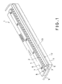
- an insulated substrate 3 on which there are arranged a plurality of semiconductor devices 2 such as electro-thermal converting elements and their wire bondings and an IC for driving them is placed in a row together with a flexible cable 4 on a support plate 5.
- the substrate 3 and the cable 4 are pressed onto the support plate 5 by a rigid holding member 6 for holding the flexible cable and five screws 7 through a rubber holder 8 so that a wiring portion of the substrate 3 and the flexible cable 4 can be fixed mechanically and connected electrically to each other.
- Reference numeral 9 denotes an ink feed pipe for feeding ink from both sides into a common liquid chamber 10.
- the ink feed pipe is composed of an elastic tube.
- a part of the common liquid chamber 10 is formed by providing a member or top plate 11 composed of a resin or the like with depressions, and a part of an ink discharge portion or orifice 12 is similarly formed thereby. By bonding these on the substrate 3 a space for flowing ink therein and openings for discharging ink therethrough are formed, thus constructing the ink jet head 1.
- Fig. 2 is a schematic perspective view illustrating a serial scanning type ink jet recording apparatus.
- the head 1 having, for example, 16 to 256 discharge portions is detachably mounted on a carriage 21 which is guided on a guide shaft 20, and in this state is scanned in a direction perpendicular to the direction in which recording paper 22 is conveyed.
- Reference numeral 23 denotes a belt conveyor for scanning the carriage 21.
- Reference numeral 24 denotes a conveyor roll and reference numeral 25 denotes a platen. These convey the recording paper 22 to a desired position.
- reference numeral 26 denotes a discharge recovering apparatus for maintaining the discharge portions in good conditions, which includes an elastic cap, an aspirator and the like.
- the system of the above-described example is constructed such that signal outputs for driving the recording paper conveying means, head scanning means and discharge recovering means as well as those for driving the recording head can be controlled by controlling means based on instruction put out from CPU of the main body of the ink jet recording apparatus.
- an electro-thermal converting element which generates thermal energy utilized for discharging ink and a wiring portion for connecting the electro-thermal converting element to the semiconductor device 2 such as IC for driving.
- a bump electrode to be connected to a solder bump provided in the semiconductor device.
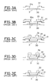
- Figs. 3A to 3E an example of the structure of the bump electrode in the conventional film wiring substrate will be explained according to its production procedures.
- a protective layer 31 composed of an inorganic insulating layer such as a SiO2 or SiN layer or an organic insulating layer such as a polyimide layer and having a circular through hole 31a.
- a barrier metal layer 32 made of, for example, Cr, Ti, Ni or the like and a solder connecting layer 33 made of, for example, Cu, Au, Cu-Au alloy or the like.
- a photoresist layer 34 Over the entire surface of the substrate 3 provided with the electrode 30, the protective layer 31, the barrier metal layer 32 and the solder connecting layer 33 is coated a photoresist layer 34 by a spin coating method, a roll coating method, a dipping method, a printing method or the like, and then exposure treatment and development treatment are performed.
- solder connecting layer 31 and the metal layer 32 are etched using the photoresist layer 34 as a mask.
- the photoresist layer 34 is peeled off to complete the procedures.
- a circular concave 33a of, for example, several centimeters or more in depth exists in the solder connecting layer 33 above the through hole 31a of the protective layer 31.
- it tends to become more difficult at every pitch of a groove of a grooved coating roll (especially, at thread portions of the roll) to carry out coating of the photoresist layer 34, resulting in that there has been a possibility that in a subsequent etching step only the through hole portions of the metal layer (i.e., the solder connecting layer 33 and in addition the barrier metal layer 32) of the concave portion 34a where coating has been carried out incompletely could be etched out.
- electro-thermal converting elements in conventional thin film wiring substrates are constructed as follows.
- Electro-thermal converting elements have heating units which convert electric energy to thermal energy to be used for discharging ink. As shown in Figs. 4A and 4B, in order to construct an electro-thermal converting element, at first an HfB2 film 40 serving as a heat generating resistor layer and an Al film serving as an electrode 41 are formed on the substrate plate 3, for example, by sputtering or the like, followed by patterning to form an electro-thermal converting element.
- an SiO2 film serving as an antioxidation film 42 and a Ta film serving as anti-cavitation film 43 for the electro-thermal converting element are formed, for example, by sputtering or the like, followed by patterning.
- the second layer i.e., Al conductive layer 41
- the second layer i.e., Al conductive layer 41
- a common electrode 45 which is Cu-plated.
- the SiO2 layer 42 and the photosensitive polyimide layer 44 underlying the common electrode 45 unction as an interlayer insulator layer.
- a plate 11 having a concave portion for forming a common liquid chamber 10 as a passage for a recording liquid and individual liquid paths 46 is bonded, and a wiring to be connected to a driving circuit which generates driving signals for driving the electro-thermal converting element is electrically connected, thus producing a liquid spray recording head.(not shown).
- Fig. 4A the heat generating resistor layer 40, the electrode 41 and the common electrode 45 are illustrated but the protective layers 42, 43 and 44 and the plate 11 are omitted.
- the electrode 41 opposite to the common electrode i.e., segment electrode
- the above-described bump electrode through which the electrode 41 is connected to a semiconductor device. It should be noted that the same is true in the case where the semiconductor device is connected to the end on the side of the common electrode 45.
- the common electrode 45 is placed outside the plate 11, more specifically outside the liquid paths of the recording head and therefore the part of the electrode 41 on the side of the common electrode 45 must have a length of M2 as shown in Figs. 4A and 4B which is considerably larger than the length M1 of the part of the electrode 41 within the plate 11 and thus a considerably long high density wiring is necessary.
- This makes severer disadvantages involved in production such as low yield due to short circuit, disconnection or the like. That is, repeated driving of the conventional device under application of a large amount of electric current which can generate heat enough to discharge liquid causes short circuit or disconnection, resulting in that the durability of the recording head decreases unacceptably.
- a second object of the present invention is to provide a recording apparatus and a recording head which have an electro-thermal converting element for discharging ink having excellent durability and thus are highly reliable and can perform high resolution recording stably.
- a third object of the present invention is to provide a recording apparatus and a recording head which can be produced in increased yields, and are small in size and cheap.
- a wiring substrate having an insulated substrate, a wiring portion arranged on the insulated substrate and with an electroconductive layer, and a protective layer provided on the electroconductive layer such that at least a part of the electroconductive layer is exposed
- the protective layer comprises at least two unit layers
- the electroconductive layers comprises at least two layers, one being positioned above the protective layers and another below the protective layers
- the protective layers are formed with respective through holes for connecting the electroconductive layer above the protective layers to the electroconductive layer below the protective layers
- the through hole of at least one of the unit protective layers has a size and shape different from those of the through hole in remaining unit protective layer(s).
- the recording head of the present invention comprises the above-described wiring substrate.
- the recording apparatus of the present invention comprises the above-described recording head and means for conveying a recording medium to a recording position where recording is performed by the recording head.
- This embodiment relates to a wiring substrate having an improved bump electrode portion.
- Figs. 5A to 5G are intended to illustrate the thin film wiring substrate according to one embodiment of the present invention and are each a cross section showing the production procedure of the bump electrode of the wiring substrate.
- the Al electrode 30 is formed on the insulated substrate 3.
- a protective layer 35 is formed which is provided with a through hole 35a of a tetragonal shape and having a size larger than the outer size of the Al electrode 30.
- a protective layer 36 is formed.
- the protective layer 36 is of a circular shape and provided with a through hole 36a having a size smaller than the outer size of the Al electrode 30.
- the thicknesses of the protective layers 35 and 36 may be enough to protect portions excepting the through hole portion of the Al electrode 30 when they are several micrometers (mm) in total, and the thickness of the protective layer 36 can be made considerably smaller than that of the protective layer 35. therefore, the thickness of the protective layer to be formed on the Al electrode 30 can naturally be made small enough.
- the barrier metal layer 32 and the solder connecting layer 33 are deposited by a known method.
- the photoresist layer 34 is coated by a roll coating method, exposed to light and developed. Upon coating the photoresist, as shown in Fig. 5D and Fig.
- the protective layer on the Al electrode 30 can be made formed to a small thickness even when it has a construction such that the thickness of the through hole portion (the thickness of the laminate within the through hole, i.e., the thicknesses of the barrier metal layer 32 + the solder connecting layer 33 + the photoresist layer 34) is the same in total as that of the conventional ones, resulting in that the circular concave portion 33a of the solder connecting layer 33 positioned within the through hole portion where it has hitherto been difficult to coat photoresists can be made extremely small in depth. Therefore, coating performance can be improved greatly by making the difference in height, or depth, of the concave portion 33a of the solder connecting layer 33.
- the protective layer of a two-layer structure makes it possible to design the shape of through holes freely; through holes may have different shapes one from another. Accordingly, the through hole in the lower layer may be of a shape corresponding to the contour of the electrode and the one in the upper layer may be of a shape suitable for the bump electrode portion.
- This construction increases the area of the through hole in the upper layer and further the area of the concave portion 33a in the solder connecting layer 33, thus making it possible to increase coating area of the photoresist and solving the problem that coating of photoresist is impossible in the conventional circular through hole portion.
- the protective layer for the Al electrode is laminated in at least two layers, number of defects such as pin-holes in the protective layer is negligibly small and it is now unnecessary to increase the thickness of the coating film excessively as has been required in protective layers of a single layer construction conventionally used, resulting in that the film thickness can be made smaller than ever, which decreases cost of materials and prevents curling or other undesirable phenomena of the substrate which could otherwise occur due to lamination of the substrate material with different kinds of materials.
- etching of the metal layer 32 is carried out, and finally, as shown in Fig. 5G, the photoresist layer 34 is peeled off to complete the procedure.
- the through hole in the upper protective layer 36 is made of a circular form and the through hole in the lower protective layer 35 is made of a tetragonal form as shown in Fig. 6, they may be made in reverse relation, that is, the through hole in the protective layer 36 is tetragonal and the through hole in the protective layer 35 is circular as shown in Figs. 7A and 7B.
- the tetragonal shape of the through hole may be selected freely; for example, it may be constructed such that one of the protective layers (the protective layer 36) is formed continuously for a plurality of electrodes 30.
- the through hole in either one of the protective layers 35 and 36 is made of a size larger than the outer size of the Al electrode 30, basically no problem will occur if it has the same size as the outer size of the Al electrode 30.
- the protective layer is made of a multilayer construction, thus maintaining as a whole a film thickness sufficient for protecting the electrode while at least one among plural layers covers the electrode around the periphery of the through hole portion.
- the kind of materials for the protective layers 35 and 36 and any type of inorganic or organic insulating film may be used.
- the substrate is constructed as follows.
- the protective layer 35 is formed of the same material and has the same film thickness as the antioxidation layer such as SiO2, SiN, SiC or the like on the heat generating resistor layer 40, and at the same time the protective layer 36 is formed of the same material and has the same film thickness as the ink resistant layer made of polyimide resin, epoxy resin or the like.
- This construction makes it easy to form the bump electrode 37 for efficiently connecting the substrate to the electrode (not shown) of a semiconductor device 2 in the same step, and also makes it possible to form an ink jet recording head having such bump electrode.
- a recording head as shown in Fig. 1 can be constructed. Further, a recording apparatus as shown in Fig. 2 can be constructed using such recording head.
- the protective layer for the Al electrode is laminated in at least two layers, number of defects such as pin-holes in the protective layer is negligibly small and it is now unnecessary to increase the thickness of the coating film excessively as has been required in protective layer of a single construction conventionally used, resulting in that the film thickness can be made smaller than ever, which decreases cost of materials and prevents curling or other undesirable phenomena of the substrate which could otherwise occur due to lamination of the substrate material with different kinds of materials
- one layer out of the two protective layers may be formed from layer having low-pattern density and low-accuracy of pattern.
- one layer out of the two protective layers may be formed by low-cost pattering method such as screen printing method.
- an SiO2 film film thickness: 2.75 mm
- an HfB2 layer layer thickness: 1,000 ⁇
- HfB2 purity: 99.9% or higher
- High frequency power 1,500 W.
- the target was changed to Ti (purity: 99.9% or higher) and sputtering was carried out under the same conditions as above excepting the following:
- Film forming time 1 hour to form a Ti layer (layer thickness: 50 ⁇ , not shown) serving as a contact layer.
- the target was changed to Al (purity: 99.9% or higher) and sputtering was carried out under the same conditions as above excepting the following:
- Film forming time 6 minutes to form an Al layer (layer thickness: 4,500 ⁇ ) serving as the electrode 30.
- etching of the Al layer was carried out using a mixture of acetic acid, phosphoric acid and nitric acid (acetic acid: 9%, phosphoric acid: 73% and nitric acid: 2%) as an etching solution.
- etching of the lamination of the HfB2 layer and the Ti layer was carried out by reactive etching in a vacuum chamber to remove the photoresist, thus completing the patterning.
- the reactive etching was performed under the following conditions:
- an SiO2 layer (layer thickness: 1.3 mm) serving as the protective layer 35 having mainly an antioxidation function was formed by sputtering in a vacuum chamber using SiO2 (purity: 99.9% or higher) as a target. Conditions of the sputtering were as follows:.
- Base pressure 8 X 10 ⁇ 4 Pa or lower
- the target was changed to Ta (purity 99.9% or higher) and sputtering was carried out under the same conditions as SiO2 excepting the following:
- Film forming time 30 minutes to form a Ta layer (layer thickness: 0.5 mm) serving as the protective layer 37a having mainly an anti-cavitation function.
- patterning was performed by lithography as described below relative to the SiO2 layer and the Ta layer.
- the same photoresist as described above was coated as a layer (layer thickness: 1.3 mm) on the Al layer, which was exposed to light, developed and baked by conventional methods.
- chemical etching of the Ta layer was carried out to form a pattern of the protective layer 37a, followed by removal of the photoresist. Conditions of the chemical etching were as follows:
- the same photoresist as described above was coated as a layer (layer thickness: 2.6 mm), which was exposed to light, developed and baked by conventional methods. Then, reactive etching of the SiO2 layer was carried out to form a pattern of the protective layer 35 including a through hole, followed by removal of the photoresist. Conditions of the reactive etching were as follows:
- a polyimide (trade name: UR3100, produced by Toray Corporation) was coated by a roll coating method to form a pattern of 2.5 mm in thickness, which was pre-baked, exposed to light, developed and post-cured by conventional methods to complete formation of the protective layer 36.
- the target was changed to Ti (purity: 99.9% or higher) and sputtering was carried out under the same conditions as described above excepting the following:
- Film forming time 10 minutes to form a Ti layer (layer thickness: 500 ⁇ ) serving as the barrier metal layer.32.
- the target was changed to Cu (purity: 99.9% or higher) and sputtering was carried out under the same conditions as the Ti formation excepting the following:
- Film forming time 4 minutes to form a Cu layer (layer thickness: 3,000 ⁇ ) serving as the solder connecting layer 33.
- patterning of lamination between the Ti layer and the Cu layer was carried out by lithography as described below.
- the same photoresist as described above was coated as a layer (layer thickness: 1.3 mm) by a roll coating method, which layer was exposed to light, developed and baked by conventional methods.
- etching of the Cu layer was carried out for 30 seconds using 10% by weight ammonium persulfate solution as an etching solution to form the solder connecting layer 33.
- etching of the Ti layer was carried out for 20 seconds using 2% by weight hydrofluoric acid solution as an etching solution to form the barrier metal layer 32, and thereafter the photoresist was removed.
- the plate 11 made of glass and provided with a concave portion serving as a wall of the passage for ink communicated to discharge portions.
- a wiring electrode (not shown) provided on the surface of the driving substrate 2 with a semiconductor cable was connected to the solder connecting layer 33 through the bump electrode 37 to form an ink jet head as shown in Fig 9.
- the ink jet head had several thousands of discharge portions each corresponding to a plurality of heat generating portions.
- the ink jet head was fitted to the main body of an ink jet apparatus and recording was performed with actually discharging ink. As a result, it was confirmed that the ink jet head obtained in this example was very excellent both from a point of view of recording quality and of durability.
- a wiring portion for connection was provided between the electrode portion and the common electrode, and in the wiring portion, protective layers are formed above and below this electroconductive layer using an organic material, making it possible to hold the connecting portion between the electrode and the wiring portion within the common liquid chamber and thus enabling shortening of the length of the continuous electrode portion greatly in accordance with reduction in space realized by the above-described construction.
- This construction decreases the occurrence of short circuit and disconnection in the wiring of the electrode portion, thus maintaining adhesion between the electroconductive layer and the protective layer.in good conditions for a prolonged period of time.
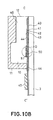
- Fig. 10A is a schematic plan view of the substrate of recording head based on the above finding of the present inventors.
- Fig. 10B is a schematic cross section of the substrate shown in Fig. 10A along the line C-C′.
- first layer is formed on the substrate plate 3 by providing thereon an HfB2 layer serving as the heat generating resistor layer 40 and an Al layer serving as the electrode 41, both used for forming an electro-thermal converting element.
- An SiO2 layer serving as the anti-oxidation film 42 of the electro-thermal converting element and a Ta layer serving as anti-cavitation film 43 are formed.
- As the ink resistant layer 44 a photosensitive polyimide is coated.
- a wiring 50 made of Al is provided as second layer (connection wiring portion).
- the protective layer 42 for the second layer 50 is coated an organic material, for example, a photosensitive polyimide.
- the common electrode 45 is made of Cu of a high electroconductivity by plating.
- the plate 11 is bonded on the substrate, and the wiring is connected electrically to construct a liquid spray recording head.
- the SiO2 layer 42 which is an interlayer insulation layer and the photosensitive polyimide layer 44 have openings having lengths of L1 and L2, respectively, where L1 > L2, and the second electroconductive layer 50 is bonded to only the photosensitive polyimide 44 and the first electroconductive layer (electrode) 41.
- the second electroconductive layer 50 is bonded to only the photosensitive polyimide 44 which is an organic material out of the underlying interlayer insulating layers.
- bonding strength between organic materials and metals is not so strong and this is no problem in initial stages.
- the bonding between the organic material and the electroconductive layer is deteriorated to decrease ink resistance, resulting in that there is a fear that corrosion occurs in the electroconductive layer and the electrode.
- This embodiment is to achieve further improvement with respect to the above-described problems.
- the opening of the through hole in the second insulating layer is made larger than the opening of the through hole in the first insulating layer in at least a part thereof.so that a portion which contacts the electroconductive layer directly and bonded thereto can be provided not only in the second insulating layer made of an organic material but also in the first insulating layer made of an inorganic material. This construction increases adhesion between the second electroconductive layer and each layer to improve durability and reliability of the wiring portion.
- the material for forming the first and second electroconductive layers there can be used Al, Cu and the like.
- the first insulating layer there can be used SiO2, SiN, SiC, Ta2O5, AlN, Al2O3, and the like while photosensitive polyimide, epoxy resin, acrylic resin, silicone resin and the like are used for the second insulating layer.
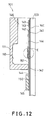
- Fig. 11 is a schematic plan view of the heat generating substrate for the recording head according to the third embodiment of the present invention.
- Fig. 12 is a schematic cross section of the substrate shown in Fig. 11 along the line A-A′.
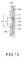
- Fig 13 is a partial enlarged view of the contact portion B of the wiring shown in Fig. 12, which illustrates well characteristic feature of the present invention.
- an HfB2 layer 140 as a heat generating resistor layer for forming an electro-thermal converting element and an Al layer 141 by sputtering and deposition, respectively, and patterned by etching to form a first electroconductive layer.
- an SiO2 layer as an anti-oxidation protective layer for the electro-thermal converting element is formed thereon by sputtering or a CVD method and further a Ta layer 143 as a protective layer having anti-cavitation property is formed.
- the Ta layer 143 is provided in a heat generating portion where bubbles are formed.
- a photosensitive polyimide 144 is coated to form an ink resistant protective layer and patterned. Thereon is formed an Al layer 150 as a second electroconductive layer by deposition, followed by patterning. Further, a protective layer 151 made of a photosensitive polyimide is coated thereon, and then patterned.
- Cu is plated thereon to a thickness on the order of 10 mm to form a common electrode 145.
- the heat generating substrate for the recording head 101 is formed.
- the SiO2 layer 142 as an inorganic protective layer and the photosensitive polyimide 144 as an organic protective layer beneath the second electroconductive layer serve as interlayer insulating layers.
- a plate 111 for forming a common liquid chamber 110 and liquid paths 146 is bonded with an adhesive or otherwise to construct a recording head.
- L1 designates the length of a side of the opening of the SiO2 layer 142
- L2 is the length of a side of the opening of the photosensitive polyimide 144.
- the openings, respectively are rectangular and the longer sides are defined L1 and L2, respectively. Of course, it is desirable that shorter sides be in a similar relationship.
- L1 and L2 meets the relationship L1 ⁇ L2 under which condition at least a part of the second electroconductive layer 150 is in a direct contact not only with the photosensitive polyimide 144 but also with the SiO2 layer 142 and bonded thereto.
- This construction improves long term durability and discharge stability, thus extremely increasing reliability even when it is used for a recording head utilizing thermal energy.
- L2 - L1 is set up to preferably 2 mm or more, and more preferably 1 mm or more.
- the thickness of the inorganic insulating layer be 0.1 to 10 mm, preferably 0.5 to 3 mm, and the thickness of the organic insulating layer be 0.5 to 3 mm, preferably 1 to 5 mm.
- the laminate structure including a bump electrode as described in Embodiment 1 is formed so that the bump electrode is positioned on the corresponding substrate plate in the common ink chamber. Thereafter, a protective layer is formed on the bump electrode using an organic material as in Embodiment 3 to make a substrate for the ink jet head according to this embodiment.
- the above-described wiring substrate, recording head and recording apparatus of the present invention are desirably applied to apparatuses of types utilizing basic operational principle disclosed, for example, in U.S. Patents Nos. 4,723129 and 4,749,796
- the principle is applicable to a so-called on-demand type recording system and a continuous type recording system, particularly it is suitable for the on-demand type because the principle is such that at least one driving signal is applied to an electro-thermal converting element disposed on liquid (ink) retaining sheet or ink passage, the driving signal being enough to provide such a quick temperature rise beyond a departure from nucleation boiling point, by which the thermal energy is provided by the electro-thermal converting element to produce film boiling on the heating portion of the recording head, whereby a bubble can be formed in the liquid (ink) corresponding to each of the driving signals.
- the liquid (ink) is discharged through an discharge portion to produce at least one droplet.
- the driving signal is preferably in the form of a pulse because the development and collapse of the bubble can be effected instantaneously, and therefore, the liquid (ink) is discharged with quick response.
- the driving signal in the form of the pulse is preferably such as disclosed in U.S. Patent Nos. 4,463,359 and 4,345,262.
- the temperature increasing rate of the heating surface is preferably such as disclosed in U.S. Patent No. 4,313,124.
- the structure of the recording head may be as shown in U.S. Patent Nos. 4,558,333 and 4,459,600 wherein the heating portion is disposed at a bent portion in addition to the structure of the combination of the discharging portion, liquid passage and the above-described patents.
- the present invention is applicable to the structure disclosed in Japanese Patent Application Laying-Open No. 123670/1984 wherein a common slit is used a discharge portion for plural electro-thermal converting elements, and to the structure disclosed in Japanese Patent Application Laying-Open No. 138461/1984 wherein an opening for absorbing pressure wave of the thermal energy is formed corresponding to the discharge portion. This is because the present invention is effective to perform the recording operation with certainty and at high efficiency irrespective of the type of the recording head.
- Such a recording head may comprise a single recording head integrally formed and a plurality recording heads combined to cover the entire width.
- the present invention is applicable to a serial type recording head wherein the recording head is fixed on the main assembly, to a replaceable chip type recording head which is connected electrically with the main apparatus and can be supplied with the ink by being mounted in the main assembly, or to a cartridge type recording head having an integral ink container.
- the recovery means and the auxiliary means for the preliminary operation are preferred because they can further stabilize the effect of the present invention.
- a single head corresponding to a single color ink may be equipped, or a plurality of heads corresponding, respectively, to a plurality of ink materials having different recording color or density may be equipped.
- the present invention is effectively applicable to an apparatus having at least one of a monochromatic mode solely with main color such as black and a multi-color mode with different color ink materials or a full-color mode by color mixture.
- the multi-color or full-color mode may be realized by a single recording head unit having a plurality of head formed integrally or by a combination of a plurality of recording heads.
- the form of the ink jet recording apparatus to which the present invention is applicable may be the one which can be used as an image output terminal for information processor such as computers and the like and in addition thereto a copying apparatus combined with a reader or the like as well as a facsimile apparatus having transmission and receiving functions.
- the ink has been liquid. It may, however, be an ink material solidified at room temperature or below and liquefied at room temperature. Since in the ink jet recording system, the ink is controlled within the temperature not less than 30°C and not more than 70°C to stabilize the viscosity of the ink to provide the stabilized discharging, in usual recording apparatus of this type, the ink is such that it is liquid within the temperature range when the recording signal is applied. In addition, the temperature rise due to the thermal energy is positively prevented by consuming it for the state change of the ink from the solid state to the liquid state, or the ink material is solidified when it is left is used to prevent the evaporation of the ink.
- the ink may be liquefied, and the liquefied ink may be discharged.
- the ink may start to be solidified at the time when it reaches the recording material.
- the present invention is applicable to such an ink material as is liquefied by the application of the thermal energy.
- Such an ink material may be retained as a liquid or solid material on through holes or recesses formed in a porous sheet as disclosed in Japanese Patent Application Laying-Open No. 56847/1979 and Japanese Patent Application Laying-Open No. 71260/1985.
- the sheet is faced to the electro-thermal converting elements.
- the most effective one for the ink materials described above is the film boiling system.
Abstract
Description
- The present invention relates to a recording system applicable to copying machines, facsimile apparatuses, word processors, printers as an output terminal for a computer or the like which system performs recording by discharging a recording ink through a discharge portion, a recording head used for the above-described recording system and a wiring substrate suitable for the recording head.
- Conventionally, full-line type ink jet recording heads having structures as illustrated, for example, in Fig. 1 have been known as a recording head.
- In the
head 1 illustrated in Fig. 1, aninsulated substrate 3 on which there are arranged a plurality ofsemiconductor devices 2 such as electro-thermal converting elements and their wire bondings and an IC for driving them is placed in a row together with aflexible cable 4 on asupport plate 5. Thesubstrate 3 and thecable 4 are pressed onto thesupport plate 5 by arigid holding member 6 for holding the flexible cable and five screws 7 through a rubber holder 8 so that a wiring portion of thesubstrate 3 and theflexible cable 4 can be fixed mechanically and connected electrically to each other.Reference numeral 9 denotes an ink feed pipe for feeding ink from both sides into a commonliquid chamber 10. The ink feed pipe is composed of an elastic tube. - A part of the common
liquid chamber 10 is formed by providing a member ortop plate 11 composed of a resin or the like with depressions, and a part of an ink discharge portion ororifice 12 is similarly formed thereby. By bonding these on the substrate 3 a space for flowing ink therein and openings for discharging ink therethrough are formed, thus constructing theink jet head 1. - On the other hand, Fig. 2 is a schematic perspective view illustrating a serial scanning type ink jet recording apparatus.
- In Fig. 2, the
head 1 having, for example, 16 to 256 discharge portions is detachably mounted on acarriage 21 which is guided on aguide shaft 20, and in this state is scanned in a direction perpendicular to the direction in which recordingpaper 22 is conveyed.Reference numeral 23 denotes a belt conveyor for scanning thecarriage 21.Reference numeral 24 denotes a conveyor roll andreference numeral 25 denotes a platen. These convey therecording paper 22 to a desired position. Further,reference numeral 26 denotes a discharge recovering apparatus for maintaining the discharge portions in good conditions, which includes an elastic cap, an aspirator and the like. - The system of the above-described example is constructed such that signal outputs for driving the recording paper conveying means, head scanning means and discharge recovering means as well as those for driving the recording head can be controlled by controlling means based on instruction put out from CPU of the main body of the ink jet recording apparatus.
- Among the above-described conventional recording heads and recording systems, what is aimed at by the present invention is an apparatus of a type which discharges ink by utilizing thermal energy since the present invention exhibits excellent effects in this type of apparatus.
- The typical structure and operational principle of this type are preferably the one disclosed in U.S. Patent Nos. 4,723,129 and 4,740,796.
- On the
wiring substrate 3 of the above-describedconventional recording head 1 are formed an electro-thermal converting element which generates thermal energy utilized for discharging ink and a wiring portion for connecting the electro-thermal converting element to thesemiconductor device 2 such as IC for driving. - In the wiring portion is provided a bump electrode to be connected to a solder bump provided in the semiconductor device.
- Referring to Figs. 3A to 3E, an example of the structure of the bump electrode in the conventional film wiring substrate will be explained according to its production procedures.
- Firstly, as shown in Fig. 3A, there are formed on the
insulated substrate 3 anAl electrode 30 and also aprotective layer 31 composed of an inorganic insulating layer such as a SiO₂ or SiN layer or an organic insulating layer such as a polyimide layer and having a circular throughhole 31a. - Subsequently, as shown in Fig. 3B, on the
substrate 1 are deposited by sputtering abarrier metal layer 32 made of, for example, Cr, Ti, Ni or the like and asolder connecting layer 33 made of, for example, Cu, Au, Cu-Au alloy or the like. - Over the entire surface of the
substrate 3 provided with theelectrode 30, theprotective layer 31, thebarrier metal layer 32 and thesolder connecting layer 33 is coated aphotoresist layer 34 by a spin coating method, a roll coating method, a dipping method, a printing method or the like, and then exposure treatment and development treatment are performed. - Thereafter, as shown Fig. 3D, the
solder connecting layer 31 and themetal layer 32 are etched using thephotoresist layer 34 as a mask. - Finally, as shown in Fig. 3E, the
photoresist layer 34 is peeled off to complete the procedures. - In the production of the above-described conventional film wiring substrate, it is generally the case that a roll coating method is selected in the step of photoresist coating in view of the fact that the substrate is of a polygon (usually tetragon) and has a large area and of productivity.
- However, in the above-described conventional film wiring substrate, as shown in Fig. 3B, a circular concave 33a of, for example, several centimeters or more in depth exists in the
solder connecting layer 33 above the throughhole 31a of theprotective layer 31. Thus, it tends to become more difficult at every pitch of a groove of a grooved coating roll (especially, at thread portions of the roll) to carry out coating of thephotoresist layer 34, resulting in that there has been a possibility that in a subsequent etching step only the through hole portions of the metal layer (i.e., thesolder connecting layer 33 and in addition the barrier metal layer 32) of the concave portion 34a where coating has been carried out incompletely could be etched out. - On the other hand, electro-thermal converting elements in conventional thin film wiring substrates are constructed as follows.
- Electro-thermal converting elements have heating units which convert electric energy to thermal energy to be used for discharging ink. As shown in Figs. 4A and 4B, in order to construct an electro-thermal converting element, at first an
HfB₂ film 40 serving as a heat generating resistor layer and an Al film serving as anelectrode 41 are formed on thesubstrate plate 3, for example, by sputtering or the like, followed by patterning to form an electro-thermal converting element. - Next, an SiO₂ film serving as an
antioxidation film 42 and a Ta film serving asanti-cavitation film 43 for the electro-thermal converting element are formed, for example, by sputtering or the like, followed by patterning. - Thereafter, a photosensitive polyimide as an ink-resistant protective film 44.is coated thereon and patterning is carried out.
- Further, the second layer, i.e., Al
conductive layer 41, is partially exposed and on this exposed portion is formed acommon electrode 45 which is Cu-plated. In this case, theSiO₂ layer 42 and thephotosensitive polyimide layer 44 underlying thecommon electrode 45 unction as an interlayer insulator layer. - Thereafter, a
plate 11 having a concave portion for forming a commonliquid chamber 10 as a passage for a recording liquid and individualliquid paths 46 is bonded, and a wiring to be connected to a driving circuit which generates driving signals for driving the electro-thermal converting element is electrically connected, thus producing a liquid spray recording head.(not shown). - In Fig. 4A, the heat generating
resistor layer 40, theelectrode 41 and thecommon electrode 45 are illustrated but theprotective layers plate 11 are omitted. - On one end of the
electrode 41 opposite to the common electrode, i.e., segment electrode, is usually formed the above-described bump electrode through which theelectrode 41 is connected to a semiconductor device. It should be noted that the same is true in the case where the semiconductor device is connected to the end on the side of thecommon electrode 45. - In the conventional technique as described above, the
common electrode 45 is placed outside theplate 11, more specifically outside the liquid paths of the recording head and therefore the part of theelectrode 41 on the side of thecommon electrode 45 must have a length of M₂ as shown in Figs. 4A and 4B which is considerably larger than the length M₁ of the part of theelectrode 41 within theplate 11 and thus a considerably long high density wiring is necessary. This makes severer disadvantages involved in production such as low yield due to short circuit, disconnection or the like. That is, repeated driving of the conventional device under application of a large amount of electric current which can generate heat enough to discharge liquid causes short circuit or disconnection, resulting in that the durability of the recording head decreases unacceptably. - Under the circumstances, the present invention has been made with view to obviating the above-described disadvantages of the prior art.
- It is a first object of the present invention to provide a thin film wiring substrate which is free of a possibility that in an etching step as a posterior step in the formation of a substrate a metal layer is etched out only on a through hole portion by improving the shape of a bump electrode portion (solder connecting layer) provided on a wiring substrate, a recording head and a recording apparatus which have such a substrate.
- A second object of the present invention is to provide a recording apparatus and a recording head which have an electro-thermal converting element for discharging ink having excellent durability and thus are highly reliable and can perform high resolution recording stably.
- A third object of the present invention is to provide a recording apparatus and a recording head which can be produced in increased yields, and are small in size and cheap.
- In order to achieve the above-described objects, according to the present invention, there is provided a wiring substrate having an insulated substrate, a wiring portion arranged on the insulated substrate and with an electroconductive layer, and a protective layer provided on the electroconductive layer such that at least a part of the electroconductive layer is exposed, wherein the protective layer comprises at least two unit layers, the electroconductive layers comprises at least two layers, one being positioned above the protective layers and another below the protective layers, the protective layers are formed with respective through holes for connecting the electroconductive layer above the protective layers to the electroconductive layer below the protective layers, the through hole of at least one of the unit protective layers has a size and shape different from those of the through hole in remaining unit protective layer(s).
- Further, the recording head of the present invention comprises the above-described wiring substrate. Also, the recording apparatus of the present invention comprises the above-described recording head and means for conveying a recording medium to a recording position where recording is performed by the recording head.
- The above and other objects, effects, features and advantages of the present invention will become more apparent from the following description of embodiments thereof taken in conjunction with the accompanying drawings.
- Fig. 1 is a perspective view of the ink jet recording head according to the present invention;
- Fig. 2 is a perspective view of the ink jet recording apparatus according to the present invention;
- Figs. 3A to 3E are cross sections illustrating the production procedures of a bump electrode in the conventional thin film wiring substrate;
- Fig. 4A is a schematic plan view illustrating the conventional recording head;
- Fig. 4B is a cross section of the conventional recording head along the line B-B′ in Fig. 4A;
- Figs. 5A to 5G are cross sections of the wiring substrate illustrating the production method for producing the bump electrode according to the present invention;
- Fig. 6 is a top view of the wiring substrate shown in Fig. 5D;.
- Figs. 7A and 7B illustrate the wiring substrate according to another embodiment of the present invention, Fig. 7A showing a top view of the laminated substrate and Fig. 7B being cross section along the line A-A′ in Fig. 7A;
- Fig. 8 is a top view of the wiring substrate according to still another embodiment of the present invention;
- Fig. 9 is a cross section of the ink jet recording head according to the present invention;
- Fig. 10A is a schematic plan view of the substrate of the recording head according to the present invention;
- Fig. 10B is a cross section of the substrate along the line C-C′ in Fig. 10A;
- Fig. 10C is a partial enlarged view of the substrate shown in Fig. 10B;
- Fig. 11 is a schematic plan view of the heat generating substrate of the recording head according to an embodiment of the present invention;
- Fig. 12 is a cross section of the substrate along the line D-D′ in Fig. 11; and
- Fig. 13 is a partial enlarged view of the contact portion E of the wiring in Fig. 12.
- This embodiment relates to a wiring substrate having an improved bump electrode portion.
- Hereafter, this embodiment will be explained in detail with reference to the attache drawings. In the drawings, the same components as those shown in Figs. 3A to 3E are indicated with the same reference numerals as used therein and their explanation are simplified herein.
- Figs. 5A to 5G are intended to illustrate the thin film wiring substrate according to one embodiment of the present invention and are each a cross section showing the production procedure of the bump electrode of the wiring substrate.
- Firstly, as shown in Fig. 5A, the
Al electrode 30 is formed on theinsulated substrate 3. Thereafter, as shown in Fig. 5B, aprotective layer 35 is formed which is provided with a throughhole 35a of a tetragonal shape and having a size larger than the outer size of theAl electrode 30. Then, as shown in Fig. 5C, aprotective layer 36 is formed. Theprotective layer 36 is of a circular shape and provided with a throughhole 36a having a size smaller than the outer size of theAl electrode 30. On this occasion, the thicknesses of theprotective layers Al electrode 30 when they are several micrometers (mm) in total, and the thickness of theprotective layer 36 can be made considerably smaller than that of theprotective layer 35. therefore, the thickness of the protective layer to be formed on theAl electrode 30 can naturally be made small enough. - Next, as shown in Fig. 5D, the
barrier metal layer 32 and thesolder connecting layer 33 are deposited by a known method. Subsequently, as shown in Fig. 5C, thephotoresist layer 34 is coated by a roll coating method, exposed to light and developed. Upon coating the photoresist, as shown in Fig. 5D and Fig. 6, the protective layer on theAl electrode 30 can be made formed to a small thickness even when it has a construction such that the thickness of the through hole portion (the thickness of the laminate within the through hole, i.e., the thicknesses of thebarrier metal layer 32 + thesolder connecting layer 33 + the photoresist layer 34) is the same in total as that of the conventional ones, resulting in that the circularconcave portion 33a of thesolder connecting layer 33 positioned within the through hole portion where it has hitherto been difficult to coat photoresists can be made extremely small in depth. Therefore, coating performance can be improved greatly by making the difference in height, or depth, of theconcave portion 33a of thesolder connecting layer 33. Use of the protective layer of a two-layer structure makes it possible to design the shape of through holes freely; through holes may have different shapes one from another. Accordingly, the through hole in the lower layer may be of a shape corresponding to the contour of the electrode and the one in the upper layer may be of a shape suitable for the bump electrode portion. This construction increases the area of the through hole in the upper layer and further the area of theconcave portion 33a in thesolder connecting layer 33, thus making it possible to increase coating area of the photoresist and solving the problem that coating of photoresist is impossible in the conventional circular through hole portion. - As described above, because the protective layer for the Al electrode is laminated in at least two layers, number of defects such as pin-holes in the protective layer is negligibly small and it is now unnecessary to increase the thickness of the coating film excessively as has been required in protective layers of a single layer construction conventionally used, resulting in that the film thickness can be made smaller than ever, which decreases cost of materials and prevents curling or other undesirable phenomena of the substrate which could otherwise occur due to lamination of the substrate material with different kinds of materials.
- After the above-described step, as shown in Fig. 5F, etching of the
metal layer 32 is carried out, and finally, as shown in Fig. 5G, thephotoresist layer 34 is peeled off to complete the procedure. - While in the above description, the through hole in the upper
protective layer 36 is made of a circular form and the through hole in the lowerprotective layer 35 is made of a tetragonal form as shown in Fig. 6, they may be made in reverse relation, that is, the through hole in theprotective layer 36 is tetragonal and the through hole in theprotective layer 35 is circular as shown in Figs. 7A and 7B. Further, the tetragonal shape of the through hole may be selected freely; for example, it may be constructed such that one of the protective layers (the protective layer 36) is formed continuously for a plurality ofelectrodes 30. While in the above description, the through hole in either one of theprotective layers Al electrode 30, basically no problem will occur if it has the same size as the outer size of theAl electrode 30. What is important is to make the thickness of the protective layer on theelectrode 30 small enough, and for this purpose, the protective layer is made of a multilayer construction, thus maintaining as a whole a film thickness sufficient for protecting the electrode while at least one among plural layers covers the electrode around the periphery of the through hole portion. There is no limitation on the kind of materials for theprotective layers - In the case where the
wired electrode substrate 3 according toEmbodiment 1 is applied to a substrate for an ink jet recording head, the substrate is constructed as follows. - Firstly, as shown in Fig. 9, the
protective layer 35 is formed of the same material and has the same film thickness as the antioxidation layer such as SiO₂, SiN, SiC or the like on the heat generatingresistor layer 40, and at the same time theprotective layer 36 is formed of the same material and has the same film thickness as the ink resistant layer made of polyimide resin, epoxy resin or the like. This construction makes it easy to form thebump electrode 37 for efficiently connecting the substrate to the electrode (not shown) of asemiconductor device 2 in the same step, and also makes it possible to form an ink jet recording head having such bump electrode. - Using the substrate as described above, a recording head as shown in Fig. 1 can be constructed. Further, a recording apparatus as shown in Fig. 2 can be constructed using such recording head.
- According to above embodiments, upon coating the photoresist for patterning of the bump electrode, even if the photoresist layer is coated by roll coating method having a high-productivity but not a better coating performance, there is no coating area being impossible to coat.
- In these embodiments, because the protective layer for the Al electrode is laminated in at least two layers, number of defects such as pin-holes in the protective layer is negligibly small and it is now unnecessary to increase the thickness of the coating film excessively as has been required in protective layer of a single construction conventionally used, resulting in that the film thickness can be made smaller than ever, which decreases cost of materials and prevents curling or other undesirable phenomena of the substrate which could otherwise occur due to lamination of the substrate material with different kinds of materials
- In these embodiments, further more, as shown in Fig. 9, one layer out of the two protective layers may be formed from layer having low-pattern density and low-accuracy of pattern. Thus, in this case, one layer out of the two protective layers may be formed by low-cost pattering method such as screen printing method.
- Based on
Embodiments - On the
substrate plate 3 made of a single crystal of Si having on its surface an SiO₂ film (film thickness: 2.75 mm) formed by thermal oxidation was formed an HfB₂ layer (layer thickness: 1,000 Å) functioning as the heat generatingresistor layer 4 by sputtering in a vacuum chamber using HfB₂ (purity: 99.9% or higher) as a target. Conditions for the sputtering were as follows. - Target area: 8 inch f
- High frequency power: 1,500 W.
- Temperature at which substrate plate is set: 100°C
- Film forming time: 20 minutes
- Base pressure: 1
X 10⁻⁵ Pa or lower - Sputtering gas: argon
- Sputtering gas pressure: 0.5 Pa
- Then, the target was changed to Ti (purity: 99.9% or higher) and sputtering was carried out under the same conditions as above excepting the following:
- Film forming time: 1 hour
to form a Ti layer (layer thickness: 50 Å, not shown) serving as a contact layer. - Further, the target was changed to Al (purity: 99.9% or higher) and sputtering was carried out under the same conditions as above excepting the following:
- High frequency power: 5,000 W
- Film forming time: 6 minutes
to form an Al layer (layer thickness: 4,500 Å)
serving as theelectrode 30. - Subsequently, patterning was performed by lithography as described below relative to the lamination of the HfB₂ layer with the Ti layer and to the Al layer. Firstly, a photoresist (trade name: OFPR800, produced by Tokyo Oka Co., Ltd.) was coated as a layer (layer thickness: 1.3 mm) on the Al layer, which was exposed to light, developed and baked by conventional methods. Then, etching of the Al layer was carried out using a mixture of acetic acid, phosphoric acid and nitric acid (acetic acid: 9%, phosphoric acid: 73% and nitric acid: 2%) as an etching solution. Thereafter, etching of the lamination of the HfB₂ layer and the Ti layer was carried out by reactive etching in a vacuum chamber to remove the photoresist, thus completing the patterning. The reactive etching was performed under the following conditions:
- Etching power: 450 W
- Etching time: 5 minutes
- Base pressure : 1
X 10⁻³ Pa - Gas species: BCl₃
- Gas pressure: 3 Pa
- Then, an SiO₂ layer (layer thickness: 1.3 mm) serving as the
protective layer 35 having mainly an antioxidation function was formed by sputtering in a vacuum chamber using SiO₂ (purity: 99.9% or higher) as a target. Conditions of the sputtering were as follows:. - Target area: 8 inch f
- High frequency power: 2,000 W.
- Temperature at which substrate plate is set: 100°C
- Film forming time: 90 minutes
- Base pressure: 8
X 10⁻⁴ Pa or lower - Sputtering gas: argon
- Sputtering gas pressure: 0.5 Pa
- Further, the target was changed to Ta (purity 99.9% or higher) and sputtering was carried out under the same conditions as SiO₂ excepting the following:
- High frequency power: 1,500 W
- Film forming time: 30 minutes
to form a Ta layer (layer thickness: 0.5 mm) serving as theprotective layer 37a having mainly an anti-cavitation function. - Subsequently, patterning was performed by lithography as described below relative to the SiO₂ layer and the Ta layer. Firstly, the same photoresist as described above was coated as a layer (layer thickness: 1.3 mm) on the Al layer, which was exposed to light, developed and baked by conventional methods. Then, chemical etching of the Ta layer was carried out to form a pattern of the
protective layer 37a, followed by removal of the photoresist. Conditions of the chemical etching were as follows: - Etching power: 600 W
- Etching time: 8 minutes
- Base pressure : 1 Pa
- Gas species: CF₄ (flow rate: 200 sccm)
- Gas species: O₂ (flow rate: 100 sccm)
- Gas pressure: 15 Pa
- Thereafter, the same photoresist as described above was coated as a layer (layer thickness: 2.6 mm), which was exposed to light, developed and baked by conventional methods. Then, reactive etching of the SiO₂ layer was carried out to form a pattern of the
protective layer 35 including a through hole, followed by removal of the photoresist. Conditions of the reactive etching were as follows: - Etching power: 950 W
- Etching time: 33 minutes
- Base pressure : 5
X 10⁻³ Pa - Gas species:
CHF₃ (flow rate: 16 sccm)
C₂F₅ (flow rate: 24 sccm)
O₂ (flow rate: 5 sccm) - Gas pressure: 2 Pa
- Next, a polyimide (trade name: UR3100, produced by Toray Corporation) was coated by a roll coating method to form a pattern of 2.5 mm in thickness, which was pre-baked, exposed to light, developed and post-cured by conventional methods to complete formation of the
protective layer 36. - Subsequently, the target was changed to Ti (purity: 99.9% or higher) and sputtering was carried out under the same conditions as described above excepting the following:
- Film forming time: 10 minutes
to form a Ti layer (layer thickness: 500 Å) serving as the barrier metal layer.32. - Further, the target was changed to Cu (purity: 99.9% or higher) and sputtering was carried out under the same conditions as the Ti formation excepting the following:
- High frequency power: 5,000 W
- Film forming time: 4 minutes
to form a Cu layer (layer thickness: 3,000 Å) serving as thesolder connecting layer 33. Subsequently, patterning of lamination between the Ti layer and the Cu layer was carried out by lithography as described below. Firstly, the same photoresist as described above was coated as a layer (layer thickness: 1.3 mm) by a roll coating method, which layer was exposed to light, developed and baked by conventional methods. Then, etching of the Cu layer was carried out for 30 seconds using 10% by weight ammonium persulfate solution as an etching solution to form thesolder connecting layer 33. Next, etching of the Ti layer was carried out for 20 seconds using 2% by weight hydrofluoric acid solution as an etching solution to form thebarrier metal layer 32, and thereafter the photoresist was removed. - On the thus-formed substrate for an ink jet head was arranged the
plate 11 made of glass and provided with a concave portion serving as a wall of the passage for ink communicated to discharge portions. - On the other hand, a wiring electrode (not shown) provided on the surface of the driving
substrate 2 with a semiconductor cable was connected to thesolder connecting layer 33 through thebump electrode 37 to form an ink jet head as shown in Fig 9. The ink jet head had several thousands of discharge portions each corresponding to a plurality of heat generating portions. - The ink jet head was fitted to the main body of an ink jet apparatus and recording was performed with actually discharging ink. As a result, it was confirmed that the ink jet head obtained in this example was very excellent both from a point of view of recording quality and of durability.
- To cope with the problem involved in the electro-thermal converting element portion explained in the description of the prior art, the following countermeasure has been found. More specifically, a wiring portion for connection was provided between the electrode portion and the common electrode, and in the wiring portion, protective layers are formed above and below this electroconductive layer using an organic material, making it possible to hold the connecting portion between the electrode and the wiring portion within the common liquid chamber and thus enabling shortening of the length of the continuous electrode portion greatly in accordance with reduction in space realized by the above-described construction.
- This construction decreases the occurrence of short circuit and disconnection in the wiring of the electrode portion, thus maintaining adhesion between the electroconductive layer and the protective layer.in good conditions for a prolonged period of time.
- Fig. 10A is a schematic plan view of the substrate of recording head based on the above finding of the present inventors. Fig. 10B is a schematic cross section of the substrate shown in Fig. 10A along the line C-C′.
- Firstly, first layer is formed on the
substrate plate 3 by providing thereon an HfB₂ layer serving as the heat generatingresistor layer 40 and an Al layer serving as theelectrode 41, both used for forming an electro-thermal converting element. An SiO2 layer serving as theanti-oxidation film 42 of the electro-thermal converting element and a Ta layer serving asanti-cavitation film 43 are formed. As the inkresistant layer 44, a photosensitive polyimide is coated. Awiring 50 made of Al is provided as second layer (connection wiring portion). - As the
protective layer 42 for thesecond layer 50 is coated an organic material, for example, a photosensitive polyimide. Thecommon electrode 45 is made of Cu of a high electroconductivity by plating. In the same manner as the recording head described above, theplate 11 is bonded on the substrate, and the wiring is connected electrically to construct a liquid spray recording head. - Here, the structure of through hole of a multilayer wiring structure is as shown in Fig. 10C. The
SiO₂ layer 42 which is an interlayer insulation layer and thephotosensitive polyimide layer 44 have openings having lengths of L₁ and L₂, respectively, where L₁ > L₂, and thesecond electroconductive layer 50 is bonded to only thephotosensitive polyimide 44 and the first electroconductive layer (electrode) 41. - However, although the above-described construction is improved more or less, the
second electroconductive layer 50 is bonded to only thephotosensitive polyimide 44 which is an organic material out of the underlying interlayer insulating layers. Generally, bonding strength between organic materials and metals is not so strong and this is no problem in initial stages. But, when recording is continued under repeatedly applying a large amount of electric current to the electro-thermal converting element so that thermal energy high enough to enable discharging of a liquid can be generated, the bonding between the organic material and the electroconductive layer is deteriorated to decrease ink resistance, resulting in that there is a fear that corrosion occurs in the electroconductive layer and the electrode. - This embodiment is to achieve further improvement with respect to the above-described problems.
- According to a preferred embodiment of the present invention, in the case where a layer structure consisting of a first insulating layer made of an inorganic material and a second insulating layer made of an organic material is used as an interlayer insulating layer between at least two electroconductive layers in view of ink resistance, the opening of the through hole in the second insulating layer is made larger than the opening of the through hole in the first insulating layer in at least a part thereof.so that a portion which contacts the electroconductive layer directly and bonded thereto can be provided not only in the second insulating layer made of an organic material but also in the first insulating layer made of an inorganic material. This construction increases adhesion between the second electroconductive layer and each layer to improve durability and reliability of the wiring portion. As the material for forming the first and second electroconductive layers, there can be used Al, Cu and the like. For the first insulating layer, there can be used SiO₂, SiN, SiC, Ta₂O₅, AlN, Al₂O₃, and the like while photosensitive polyimide, epoxy resin, acrylic resin, silicone resin and the like are used for the second insulating layer.
- Fig. 11 is a schematic plan view of the heat generating substrate for the recording head according to the third embodiment of the present invention.
- Fig. 12 is a schematic cross section of the substrate shown in Fig. 11 along the line A-A′. Fig 13 is a partial enlarged view of the contact portion B of the wiring shown in Fig. 12, which illustrates well characteristic feature of the present invention.
- First, the production method of a
recording head 101 will be explained below. - On a
substrate plate 103 made of a single crystal of silicon are formed anHfB₂ layer 140 as a heat generating resistor layer for forming an electro-thermal converting element and anAl layer 141 by sputtering and deposition, respectively, and patterned by etching to form a first electroconductive layer. - Next, an SiO₂ layer as an anti-oxidation protective layer for the electro-thermal converting element is formed thereon by sputtering or a CVD method and further a
Ta layer 143 as a protective layer having anti-cavitation property is formed. On this occasion, it is sufficient that theTa layer 143 is provided in a heat generating portion where bubbles are formed. - Then, a
photosensitive polyimide 144 is coated to form an ink resistant protective layer and patterned. Thereon is formed anAl layer 150 as a second electroconductive layer by deposition, followed by patterning. Further, aprotective layer 151 made of a photosensitive polyimide is coated thereon, and then patterned. - In order to increase the conductivity to enable application of a large amount of electric current, Cu is plated thereon to a thickness on the order of 10 mm to form a
common electrode 145. Thus, the heat generating substrate for therecording head 101 is formed. - Here, the
SiO₂ layer 142 as an inorganic protective layer and thephotosensitive polyimide 144 as an organic protective layer beneath the second electroconductive layer (here designated by reference numeral 150) serve as interlayer insulating layers. - Thereafter, a
plate 111 for forming acommon liquid chamber 110 andliquid paths 146 is bonded with an adhesive or otherwise to construct a recording head. - The structure of the through hole portion of the multilayer wiring si as shown in fig. 12. L₁ designates the length of a side of the opening of the
SiO₂ layer 142, and L₂ is the length of a side of the opening of thephotosensitive polyimide 144. Her, the openings, respectively, are rectangular and the longer sides are defined L₁ and L₂, respectively. Of course, it is desirable that shorter sides be in a similar relationship. - According to this embodiment, L₁ and L₂ meets the relationship L₁ < L₂ under which condition at least a part of the
second electroconductive layer 150 is in a direct contact not only with thephotosensitive polyimide 144 but also with theSiO₂ layer 142 and bonded thereto. - This construction improves long term durability and discharge stability, thus extremely increasing reliability even when it is used for a recording head utilizing thermal energy.
- Further investigation by the present inventors on the relationship between L₁ and L₂ has revealed that favorable results can be obtained when L2 - L1 is set up to preferably 2 mm or more, and more preferably 1 mm or more.
- Further, in view of the problem involved in step coverage capability of the second electroconductive layer, it is desirable that the thickness of the inorganic insulating layer be 0.1 to 10 mm, preferably 0.5 to 3 mm, and the thickness of the organic insulating layer be 0.5 to 3 mm, preferably 1 to 5 mm.
- The laminate structure including a bump electrode as described in
Embodiment 1 is formed so that the bump electrode is positioned on the corresponding substrate plate in the common ink chamber. Thereafter, a protective layer is formed on the bump electrode using an organic material as inEmbodiment 3 to make a substrate for the ink jet head according to this embodiment. - On the substrate for ink jet head thus prepared are formed walls of ink paths communicated to discharge portions using a photosensitive resin, and a glass plate is provided thereon to make an ink jet recording head.
- as described earlier, the above-described wiring substrate, recording head and recording apparatus of the present invention are desirably applied to apparatuses of types utilizing basic operational principle disclosed, for example, in U.S. Patents Nos. 4,723129 and 4,749,796 The principle is applicable to a so-called on-demand type recording system and a continuous type recording system, particularly it is suitable for the on-demand type because the principle is such that at least one driving signal is applied to an electro-thermal converting element disposed on liquid (ink) retaining sheet or ink passage, the driving signal being enough to provide such a quick temperature rise beyond a departure from nucleation boiling point, by which the thermal energy is provided by the electro-thermal converting element to produce film boiling on the heating portion of the recording head, whereby a bubble can be formed in the liquid (ink) corresponding to each of the driving signals. By the development and collapse of the bubble, the liquid (ink) is discharged through an discharge portion to produce at least one droplet. The driving signal is preferably in the form of a pulse because the development and collapse of the bubble can be effected instantaneously, and therefore, the liquid (ink) is discharged with quick response. the driving signal in the form of the pulse is preferably such as disclosed in U.S. Patent Nos. 4,463,359 and 4,345,262. In addition, the temperature increasing rate of the heating surface is preferably such as disclosed in U.S. Patent No. 4,313,124.
- The structure of the recording head may be as shown in U.S. Patent Nos. 4,558,333 and 4,459,600 wherein the heating portion is disposed at a bent portion in addition to the structure of the combination of the discharging portion, liquid passage and the above-described patents. In addition, the present invention is applicable to the structure disclosed in Japanese Patent Application Laying-Open No. 123670/1984 wherein a common slit is used a discharge portion for plural electro-thermal converting elements, and to the structure disclosed in Japanese Patent Application Laying-Open No. 138461/1984 wherein an opening for absorbing pressure wave of the thermal energy is formed corresponding to the discharge portion. This is because the present invention is effective to perform the recording operation with certainty and at high efficiency irrespective of the type of the recording head.
- Further, the present invention is effectively applicable to a so-called full-line type recording head having a length corresponding to the maximum recording width and having a thousand of discharging portions or over. Such a recording head may comprise a single recording head integrally formed and a plurality recording heads combined to cover the entire width.
- In addition, the present invention is applicable to a serial type recording head wherein the recording head is fixed on the main assembly, to a replaceable chip type recording head which is connected electrically with the main apparatus and can be supplied with the ink by being mounted in the main assembly, or to a cartridge type recording head having an integral ink container.
- The provision of the recovery means and the auxiliary means for the preliminary operation are preferred because they can further stabilize the effect of the present invention. As for such means, there are capping means for the recording head, cleaning means therefor, pressing or sucking means, preliminary heating means by the discharging electro-thermal converting element and additional heating element and means for preliminary discharge not for the recording operation, which can stabilize the recording operation.
- As regards the kind and the number of the recording heads mounted, a single head corresponding to a single color ink may be equipped, or a plurality of heads corresponding, respectively, to a plurality of ink materials having different recording color or density may be equipped. The present invention is effectively applicable to an apparatus having at least one of a monochromatic mode solely with main color such as black and a multi-color mode with different color ink materials or a full-color mode by color mixture. The multi-color or full-color mode may be realized by a single recording head unit having a plurality of head formed integrally or by a combination of a plurality of recording heads.
- Furthermore, the form of the ink jet recording apparatus to which the present invention is applicable may be the one which can be used as an image output terminal for information processor such as computers and the like and in addition thereto a copying apparatus combined with a reader or the like as well as a facsimile apparatus having transmission and receiving functions.
- Still further, in the foregoing embodiment,the ink has been liquid. It may, however, be an ink material solidified at room temperature or below and liquefied at room temperature. Since in the ink jet recording system, the ink is controlled within the temperature not less than 30°C and not more than 70°C to stabilize the viscosity of the ink to provide the stabilized discharging, in usual recording apparatus of this type, the ink is such that it is liquid within the temperature range when the recording signal is applied. In addition, the temperature rise due to the thermal energy is positively prevented by consuming it for the state change of the ink from the solid state to the liquid state, or the ink material is solidified when it is left is used to prevent the evaporation of the ink. In either of the cases, the application of the recording signal producing thermal energy, the ink may be liquefied, and the liquefied ink may be discharged. The ink may start to be solidified at the time when it reaches the recording material. The present invention is applicable to such an ink material as is liquefied by the application of the thermal energy. Such an ink material may be retained as a liquid or solid material on through holes or recesses formed in a porous sheet as disclosed in Japanese Patent Application Laying-Open No. 56847/1979 and Japanese Patent Application Laying-Open No. 71260/1985. The sheet is faced to the electro-thermal converting elements. The most effective one for the ink materials described above is the film boiling system.
- The invention has been described in detail with respect to embodiments, and it will now be apparent from the foregoing to those skilled in the art that changes and modifications may be made without departing from the invention in its broader aspects, and it is the invention, therefore, in the appended claims to cover all such changes and modifications as fall within the true spirit of the invention.
Claims (20)
- A wiring substrate having an insulated substrate, a wiring portion arranged on the insulated substrate and with an electroconductive layer, and an interlayer protective layer provided on the electroconductive layer such that at least a part of the electroconductive layer is exposed, characterized in that said protective layer comprises at least two unit layers, said electroconductive layers comprises at least two layers, one being positioned above said protective layer and another below said protective layer, said unit protective layers are formed with respective through holes for connecting said electroconductive layer above said protective layer to said electroconductive layer below said protective layer, said through hole of at least one of said unit protective layers has a size and shape different from those of said through hole in at least one remaining unit protective layer.
- The wiring substrate as claimed in claim 1, characterized in that said electroconductive layer above said protective layer of said wiring portion is a bump electrode which is connected to a semiconductor device arranged on said insulted substrate.
- The wiring substrate as claimed in claim 1, characterized in that said electroconductive layer below said protective layer of said wiring portion is an electrode of an electro-thermal converting element provided on said insulated substrate, and said electroconductive layer above said protective layer is a wiring for connecting to said electrode, and wherein said interlayer protective layer comprises a first layer composed of an inorganic material and a second layer provided on said first layer and composed of an organic material.
- The wiring substrate as claimed in claim 3, characterized in that first and second layers are provided with respective through holes, the through hole in said second layer is larger than the through hole in said first layer.
- A recording head including a wiring substrate having an insulated substrate, a wiring portion arranged on the insulated substrate and with an electroconductive layer, and an interlayer protective layer provided on the electroconductive layer such that at least a part of the electroconductive layer is exposed, characterized in that said protective layer comprises at least two unit layers, said electroconductive layers comprises at least two layers, one being positioned above said protective layer and another below said protective layer, said unit protective layers are formed with respective through holes for connecting said electroconductive layer above said protective layer to said electroconductive layer below said protective layer, said through hole of at least one of said unit protective layers has a size and shape different from those of said through hole in at least one remaining unit protective layer.
- The recording head as claimed in claim 5, characterized in that said electroconductive layer above said protective layer of said wiring portion is a bump electrode which is connected to a semiconductor device arranged on said insulted substrate.
- The recording head as claimed in claim 5, characterized in that of said unit protective layers, said protective layer overlapping said electroconductive layer has a thickness smaller than that of other protective layer.
- The recording head as claimed in claim 5, characterized in that said electroconductive layer below said protective layer of said wiring portion is an electrode of an electro-thermal converting element provided on said insulated substrate, and said electroconductive layer above said protective layer is a wiring for connecting to said electrode, and wherein said interlayer protective layer comprises a first layer composed of an inorganic material and a second layer provided on said first layer and composed of an organic material.
- The recording head as claimed in claim 8, further characterized by comprising;
liquid discharging portions for discharging a liquid utilizing thermal energy generated by said electro-thermal converting element;
a plurality of liquid paths communicated to said liquid discharging portions; and
a liquid chamber communicated to said plurality of liquid paths. - The recording head as claimed in claim 9, characterized in that said through hole is positioned on said insulated substrate at a position corresponding to said liquid chamber.
- The recording head as claimed in claim 8, characterized in that first and second layers are provided with respective through holes, the through hole in said second layer is larger than the through hole in said
- A recording apparatus provided with a recording head including a wiring substrate having an insulated substrate, a wiring portion arranged on the insulated substrate and with an electroconductive layer, and an interlayer protective layer formed on the electroconductive layer such that at least a part of the electroconductive layer is exposed, and conveying means for conveying a recording medium to a recording position where recording is performed by the recording head, characterized in that said protective layer comprises at least two unit layers, said electroconductive layers comprises at least two layers, one being positioned above said protective layer and another below said protective layer, said unit protective layers are formed with respective through holes for connecting said electroconductive layer above said protective layer to said electroconductive layer below said protective layer, said through hole of at least one of said unit protective layers has a size and shape different from those of said through hole in at least one remaining unit protective layer.
- The recording apparatus as claimed in claim 12, characterized in that said electroconductive layer above said protective layer of said wiring portion is a bump electrode which is connected to a semiconductor device arranged on said insulted substrate.
- The recording head as claimed in claim 12, characterized in that of said unit protective layers, said protective layer overlapping said electroconductive layer has a thickness smaller than that of other protective layer.
- The recording apparatus as claimed in claim 12, characterized in that said electroconductive layer below said protective layer of said wiring portion is an electrode of an electro-thermal converting element provided on said insulated substrate, and said electroconductive layer above said protective layer is a wiring for connecting to said electrode, and wherein said interlayer protective layer comprises a first layer composed of an inorganic material and a second layer provided on said first layer and composed of an organic material.
- The recording apparatus as claimed in claim 15, further characterized by comprising;
liquid discharging portions for discharging a liquid utilizing thermal energy generated by said electro-thermal converting element;
a plurality of liquid paths communicated to said liquid discharging portions; and
a liquid chamber communicated to said plurality of liquid paths. - The recording head as claimed in claim 15, characterized in that said through hole is positioned on said insulated substrate at a position corresponding to said liquid chamber.
- The recording apparatus as claimed in claim 15, characterized in that first and second layers are provided with respective through holes, the through hole in said second layer is larger than the through hole in said first layer.
- An electrical wiring pattern in which an electrical conductor has an insulating layer formed over it, and is connected to another electrical conductor through an aperture in the insulating layer, the insulating layer having a reduced thickness portion at the edge of the aperture.
- An electrical wiring pattern according to claim 19 in which the insulating layer comprises first and second sub-layers, the first sub-layer being present and the second sub-layer being absent at the said reduced thickness portion.
Applications Claiming Priority (4)
| Application Number | Priority Date | Filing Date | Title |
|---|---|---|---|
| JP2042533A JP2726137B2 (en) | 1990-02-26 | 1990-02-26 | Wiring electrode substrate, ink jet recording head and ink jet recording apparatus having the wiring electrode substrate |
| JP42533/90 | 1990-02-26 | ||
| JP49873/90 | 1990-02-28 | ||
| JP2049873A JP2771008B2 (en) | 1990-02-28 | 1990-02-28 | Recording device and recording head |
Publications (3)
| Publication Number | Publication Date |
|---|---|
| EP0451939A2 true EP0451939A2 (en) | 1991-10-16 |
| EP0451939A3 EP0451939A3 (en) | 1991-12-11 |
| EP0451939B1 EP0451939B1 (en) | 1996-01-17 |
Family
ID=26382245
Family Applications (1)
| Application Number | Title | Priority Date | Filing Date |
|---|---|---|---|
| EP91301490A Expired - Lifetime EP0451939B1 (en) | 1990-02-26 | 1991-02-25 | Recording apparatus with a recording head having a wiring substrate |
Country Status (4)
| Country | Link |
|---|---|
| EP (1) | EP0451939B1 (en) |
| AT (1) | ATE133111T1 (en) |
| DE (1) | DE69116414T2 (en) |
| ES (1) | ES2082129T3 (en) |
Citations (4)
| Publication number | Priority date | Publication date | Assignee | Title |
|---|---|---|---|---|
| JPS5619639A (en) * | 1979-07-27 | 1981-02-24 | Hitachi Ltd | Semiconductor device |
| EP0344809A1 (en) * | 1988-06-03 | 1989-12-06 | Canon Kabushiki Kaisha | Liquid emission recording head, substrate therefor and liquid emission recording apparatus utilizing said head |
| EP0352142A2 (en) * | 1988-07-22 | 1990-01-24 | Canon Kabushiki Kaisha | Ink jet recording |
| EP0380366A2 (en) * | 1989-01-27 | 1990-08-01 | Canon Kabushiki Kaisha | Substrate for recording head and recording head |
-
1991
- 1991-02-25 ES ES91301490T patent/ES2082129T3/en not_active Expired - Lifetime
- 1991-02-25 AT AT91301490T patent/ATE133111T1/en not_active IP Right Cessation
- 1991-02-25 EP EP91301490A patent/EP0451939B1/en not_active Expired - Lifetime
- 1991-02-25 DE DE69116414T patent/DE69116414T2/en not_active Expired - Lifetime
Patent Citations (4)
| Publication number | Priority date | Publication date | Assignee | Title |
|---|---|---|---|---|
| JPS5619639A (en) * | 1979-07-27 | 1981-02-24 | Hitachi Ltd | Semiconductor device |
| EP0344809A1 (en) * | 1988-06-03 | 1989-12-06 | Canon Kabushiki Kaisha | Liquid emission recording head, substrate therefor and liquid emission recording apparatus utilizing said head |
| EP0352142A2 (en) * | 1988-07-22 | 1990-01-24 | Canon Kabushiki Kaisha | Ink jet recording |
| EP0380366A2 (en) * | 1989-01-27 | 1990-08-01 | Canon Kabushiki Kaisha | Substrate for recording head and recording head |
Non-Patent Citations (1)
| Title |
|---|
| PATENT ABSTRACTS OF JAPAN, vol. 5, no. 70 (E-56)[742] May 12, 1981; & JP-A-56 019 639 (AKIHIRO TOMOSAWA ET AL.) February 24, 1981 * |
Also Published As
| Publication number | Publication date |
|---|---|
| ATE133111T1 (en) | 1996-02-15 |
| EP0451939B1 (en) | 1996-01-17 |
| EP0451939A3 (en) | 1991-12-11 |
| DE69116414D1 (en) | 1996-02-29 |
| DE69116414T2 (en) | 1996-06-05 |
| ES2082129T3 (en) | 1996-03-16 |
Similar Documents
| Publication | Publication Date | Title |
|---|---|---|
| US5227812A (en) | Liquid jet recording head with bump connector wiring | |
| US5877791A (en) | Heat generating type ink-jet print head | |
| US4922269A (en) | Liquid jet recording head unit, method of making same and liquid jet recording apparatus incorporating same | |
| JP2960065B2 (en) | Inkjet print head | |
| EP1874543B1 (en) | Liquid discharge head, ink jet recording head and ink jet recording apparatus | |
| US5697144A (en) | Method of producing a head for the printer | |
| US6609783B1 (en) | Ink jet recording head, method for producing the same and recording apparatus equipped with the same | |
| US4931813A (en) | Ink jet head incorporating a thick unpassivated TaAl resistor | |
| EP0698494A2 (en) | Method for producing substrate for ink jet recording head, ink jet recording head and ink jet recording apparatus | |
| US5608435A (en) | Method for producing ink jet head having a plated bump-shaped electrode | |
| JP4617145B2 (en) | Manufacturing method of substrate for liquid discharge head | |
| EP1099555B1 (en) | Ink jet print head and ink jet printing apparatus using the same | |
| EP0380366B1 (en) | Substrate for recording head and recording head | |
| EP0352142B1 (en) | Ink jet recording | |
| EP1100684B1 (en) | Ink-jet printer head and manufacturing method thereof | |
| EP0451939A2 (en) | Recording apparatus with a recording head having a wiring substrate | |
| JPS6116862A (en) | Liquid injection recording head | |
| JP4107496B2 (en) | Ink jet print head and manufacturing method thereof | |
| US11305531B2 (en) | Liquid ejection head and liquid ejecting apparatus | |
| JP4143173B2 (en) | Ink jet recording element and ink jet recording apparatus using the same | |
| JP2771008B2 (en) | Recording device and recording head | |
| JP2001038919A (en) | Production of ink jet head | |
| JP2726137B2 (en) | Wiring electrode substrate, ink jet recording head and ink jet recording apparatus having the wiring electrode substrate | |
| CN114801503A (en) | Thermal print head, thermal printer, and method for manufacturing thermal print head | |
| JP2022112463A (en) | Thermal print head, thermal printer and thermal print head manufacturing method |
Legal Events
| Date | Code | Title | Description |
|---|---|---|---|
| PUAI | Public reference made under article 153(3) epc to a published international application that has entered the european phase |
Free format text: ORIGINAL CODE: 0009012 |
|
| AK | Designated contracting states |
Kind code of ref document: A2 Designated state(s): AT BE CH DE DK ES FR GB GR IT LI LU NL SE |
|
| PUAL | Search report despatched |
Free format text: ORIGINAL CODE: 0009013 |
|
| AK | Designated contracting states |
Kind code of ref document: A3 Designated state(s): AT BE CH DE DK ES FR GB GR IT LI LU NL SE |
|
| 17P | Request for examination filed |
Effective date: 19920427 |
|
| 17Q | First examination report despatched |
Effective date: 19920703 |
|
| GRAA | (expected) grant |
Free format text: ORIGINAL CODE: 0009210 |
|
| AK | Designated contracting states |
Kind code of ref document: B1 Designated state(s): AT BE CH DE DK ES FR GB GR IT LI LU NL SE |
|
| PG25 | Lapsed in a contracting state [announced via postgrant information from national office to epo] |
Ref country code: AT Effective date: 19960117 Ref country code: BE Effective date: 19960117 Ref country code: GR Free format text: LAPSE BECAUSE OF FAILURE TO SUBMIT A TRANSLATION OF THE DESCRIPTION OR TO PAY THE FEE WITHIN THE PRESCRIBED TIME-LIMIT Effective date: 19960117 Ref country code: CH Free format text: LAPSE BECAUSE OF FAILURE TO SUBMIT A TRANSLATION OF THE DESCRIPTION OR TO PAY THE FEE WITHIN THE PRESCRIBED TIME-LIMIT Effective date: 19960117 Ref country code: LI Free format text: LAPSE BECAUSE OF FAILURE TO SUBMIT A TRANSLATION OF THE DESCRIPTION OR TO PAY THE FEE WITHIN THE PRESCRIBED TIME-LIMIT Effective date: 19960117 Ref country code: NL Free format text: LAPSE BECAUSE OF FAILURE TO SUBMIT A TRANSLATION OF THE DESCRIPTION OR TO PAY THE FEE WITHIN THE PRESCRIBED TIME-LIMIT Effective date: 19960117 Ref country code: DK Effective date: 19960117 |
|
| REF | Corresponds to: |
Ref document number: 133111 Country of ref document: AT Date of ref document: 19960215 Kind code of ref document: T |
|
| PG25 | Lapsed in a contracting state [announced via postgrant information from national office to epo] |
Ref country code: LU Free format text: LAPSE BECAUSE OF NON-PAYMENT OF DUE FEES Effective date: 19960229 |
|
| REF | Corresponds to: |
Ref document number: 69116414 Country of ref document: DE Date of ref document: 19960229 |
|
| REG | Reference to a national code |
Ref country code: ES Ref legal event code: FG2A Ref document number: 2082129 Country of ref document: ES Kind code of ref document: T3 |
|
| ET | Fr: translation filed | ||
| ITF | It: translation for a ep patent filed |
Owner name: SOCIETA' ITALIANA BREVETTI S.P.A. |
|
| PG25 | Lapsed in a contracting state [announced via postgrant information from national office to epo] |
Ref country code: SE Effective date: 19960417 |
|
| NLV1 | Nl: lapsed or annulled due to failure to fulfill the requirements of art. 29p and 29m of the patents act | ||
| REG | Reference to a national code |
Ref country code: CH Ref legal event code: PL |
|
| PLBE | No opposition filed within time limit |
Free format text: ORIGINAL CODE: 0009261 |
|
| STAA | Information on the status of an ep patent application or granted ep patent |
Free format text: STATUS: NO OPPOSITION FILED WITHIN TIME LIMIT |
|
| 26N | No opposition filed | ||
| REG | Reference to a national code |
Ref country code: GB Ref legal event code: IF02 |
|
| PGFP | Annual fee paid to national office [announced via postgrant information from national office to epo] |
Ref country code: ES Payment date: 20040203 Year of fee payment: 14 |
|
| PG25 | Lapsed in a contracting state [announced via postgrant information from national office to epo] |
Ref country code: ES Free format text: LAPSE BECAUSE OF NON-PAYMENT OF DUE FEES Effective date: 20050226 |
|
| REG | Reference to a national code |
Ref country code: ES Ref legal event code: FD2A Effective date: 20050226 |
|
| PGFP | Annual fee paid to national office [announced via postgrant information from national office to epo] |
Ref country code: IT Payment date: 20090205 Year of fee payment: 19 |
|
| PGFP | Annual fee paid to national office [announced via postgrant information from national office to epo] |
Ref country code: FR Payment date: 20090223 Year of fee payment: 19 |
|
| PGFP | Annual fee paid to national office [announced via postgrant information from national office to epo] |
Ref country code: GB Payment date: 20100219 Year of fee payment: 20 Ref country code: DE Payment date: 20100228 Year of fee payment: 20 |
|
| REG | Reference to a national code |
Ref country code: FR Ref legal event code: ST Effective date: 20101029 |
|
| PG25 | Lapsed in a contracting state [announced via postgrant information from national office to epo] |
Ref country code: FR Free format text: LAPSE BECAUSE OF NON-PAYMENT OF DUE FEES Effective date: 20100301 |
|
| REG | Reference to a national code |
Ref country code: DE Ref legal event code: R071 Ref document number: 69116414 Country of ref document: DE |
|
| REG | Reference to a national code |
Ref country code: GB Ref legal event code: PE20 Expiry date: 20110224 |
|
| PG25 | Lapsed in a contracting state [announced via postgrant information from national office to epo] |
Ref country code: IT Free format text: LAPSE BECAUSE OF NON-PAYMENT OF DUE FEES Effective date: 20100225 |
|
| PG25 | Lapsed in a contracting state [announced via postgrant information from national office to epo] |
Ref country code: GB Free format text: LAPSE BECAUSE OF EXPIRATION OF PROTECTION Effective date: 20110224 |
|
| PG25 | Lapsed in a contracting state [announced via postgrant information from national office to epo] |
Ref country code: DE Free format text: LAPSE BECAUSE OF EXPIRATION OF PROTECTION Effective date: 20110225 |