EP0449310B1 - On-chip voltage regulator and semiconductor memory device using the same - Google Patents
On-chip voltage regulator and semiconductor memory device using the same Download PDFInfo
- Publication number
- EP0449310B1 EP0449310B1 EP91105071A EP91105071A EP0449310B1 EP 0449310 B1 EP0449310 B1 EP 0449310B1 EP 91105071 A EP91105071 A EP 91105071A EP 91105071 A EP91105071 A EP 91105071A EP 0449310 B1 EP0449310 B1 EP 0449310B1
- Authority
- EP
- European Patent Office
- Prior art keywords
- voltage
- regulator
- gate
- transistor
- chip
- Prior art date
- Legal status (The legal status is an assumption and is not a legal conclusion. Google has not performed a legal analysis and makes no representation as to the accuracy of the status listed.)
- Expired - Lifetime
Links
- 239000004065 semiconductor Substances 0.000 title claims description 10
- 102100040862 Dual specificity protein kinase CLK1 Human genes 0.000 claims description 30
- 239000000758 substrate Substances 0.000 claims description 21
- 239000003990 capacitor Substances 0.000 claims description 13
- 230000008859 change Effects 0.000 claims description 9
- 101000749294 Homo sapiens Dual specificity protein kinase CLK1 Proteins 0.000 claims description 8
- 230000007704 transition Effects 0.000 claims description 7
- 230000001360 synchronised effect Effects 0.000 claims description 3
- 238000001514 detection method Methods 0.000 claims description 2
- 238000009792 diffusion process Methods 0.000 claims 10
- 230000005669 field effect Effects 0.000 claims 10
- 230000001419 dependent effect Effects 0.000 claims 1
- 238000010586 diagram Methods 0.000 description 13
- 230000003247 decreasing effect Effects 0.000 description 8
- 238000013459 approach Methods 0.000 description 5
- 230000007423 decrease Effects 0.000 description 5
- 230000006870 function Effects 0.000 description 5
- 230000000694 effects Effects 0.000 description 4
- 230000001105 regulatory effect Effects 0.000 description 4
- 230000001276 controlling effect Effects 0.000 description 3
- XUIMIQQOPSSXEZ-UHFFFAOYSA-N Silicon Chemical compound [Si] XUIMIQQOPSSXEZ-UHFFFAOYSA-N 0.000 description 2
- 230000010354 integration Effects 0.000 description 2
- 230000004044 response Effects 0.000 description 2
- 229910052710 silicon Inorganic materials 0.000 description 2
- 239000010703 silicon Substances 0.000 description 2
- 230000003321 amplification Effects 0.000 description 1
- 230000015556 catabolic process Effects 0.000 description 1
- 239000002131 composite material Substances 0.000 description 1
- 238000007796 conventional method Methods 0.000 description 1
- 238000007599 discharging Methods 0.000 description 1
- 238000003199 nucleic acid amplification method Methods 0.000 description 1
- 230000010355 oscillation Effects 0.000 description 1
- 230000003071 parasitic effect Effects 0.000 description 1
- 238000012545 processing Methods 0.000 description 1
- 238000012546 transfer Methods 0.000 description 1
Images


Classifications
-
- G—PHYSICS
- G11—INFORMATION STORAGE
- G11C—STATIC STORES
- G11C11/00—Digital stores characterised by the use of particular electric or magnetic storage elements; Storage elements therefor
- G11C11/21—Digital stores characterised by the use of particular electric or magnetic storage elements; Storage elements therefor using electric elements
- G11C11/34—Digital stores characterised by the use of particular electric or magnetic storage elements; Storage elements therefor using electric elements using semiconductor devices
- G11C11/40—Digital stores characterised by the use of particular electric or magnetic storage elements; Storage elements therefor using electric elements using semiconductor devices using transistors
- G11C11/401—Digital stores characterised by the use of particular electric or magnetic storage elements; Storage elements therefor using electric elements using semiconductor devices using transistors forming cells needing refreshing or charge regeneration, i.e. dynamic cells
- G11C11/4063—Auxiliary circuits, e.g. for addressing, decoding, driving, writing, sensing or timing
- G11C11/407—Auxiliary circuits, e.g. for addressing, decoding, driving, writing, sensing or timing for memory cells of the field-effect type
-
- G—PHYSICS
- G11—INFORMATION STORAGE
- G11C—STATIC STORES
- G11C5/00—Details of stores covered by group G11C11/00
- G11C5/14—Power supply arrangements, e.g. power down, chip selection or deselection, layout of wirings or power grids, or multiple supply levels
- G11C5/147—Voltage reference generators, voltage or current regulators; Internally lowered supply levels; Compensation for voltage drops
-
- G—PHYSICS
- G05—CONTROLLING; REGULATING
- G05F—SYSTEMS FOR REGULATING ELECTRIC OR MAGNETIC VARIABLES
- G05F1/00—Automatic systems in which deviations of an electric quantity from one or more predetermined values are detected at the output of the system and fed back to a device within the system to restore the detected quantity to its predetermined value or values, i.e. retroactive systems
- G05F1/10—Regulating voltage or current
- G05F1/46—Regulating voltage or current wherein the variable actually regulated by the final control device is dc
- G05F1/462—Regulating voltage or current wherein the variable actually regulated by the final control device is dc as a function of the requirements of the load, e.g. delay, temperature, specific voltage/current characteristic
- G05F1/465—Internal voltage generators for integrated circuits, e.g. step down generators
-
- G—PHYSICS
- G11—INFORMATION STORAGE
- G11C—STATIC STORES
- G11C5/00—Details of stores covered by group G11C11/00
- G11C5/14—Power supply arrangements, e.g. power down, chip selection or deselection, layout of wirings or power grids, or multiple supply levels
Definitions
- the present invention generally relates to semiconductor integrated circuits, and more particularly to an on-chip voltage regulator for controlling the generation of an internal power supply voltage from an external power supply voltage.
- the first approach is to produce a transistor having a gate length of approximately 0.8 micrometers which is enough to withstand a high power supply voltage equal to, for example, 5 volts.
- the second approach is to produce a transistor having a gate length of approximately 0.5 micrometers which is suitable for a decreased power supply voltage equal to, for example, 3.3 volts. It should be noted that the transistor produced by the second approach can operate faster than that produced by the first approach.
- the power supply voltage should be decreased to a suitable voltage as the integration density increases.
- many IC chips are designed to receive a standardized external power supply voltage equal to 5 volts. Thus, it is necessary to generate a suitably dropped power supply voltage from the standardized external power supply voltage inside of each IC chip.
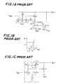
- FIG.1A is a circuit diagram of a conventional on-chip voltage regulator designed to generate, from an external voltage, an in-chip voltage lower than the external voltage.
- a regulator transistor Q1 functions as a series control regulator with respect to an external power supply voltage V EXT equal to, for example, 5 volts.
- the regulator transistor Q1 generates an internal power supply voltage V INT equal to, for example, 3.3 volts from the 5.0V external power supply voltage V EXT .
- the gate of the regulator transistor Q1 is charged by a voltage obtained by rectifying an A.C. signal generated by a ring oscillator OSC.
- the gate voltage now labeled V G1 is clamped at a fixed voltage due to the function of a transistor Q4 because the source of the transistor Q4 is set to a reference voltage V REF .
- the reference voltage V REF can be generated by a conventional method, for example, by using the threshold voltage of a MOS transistor.
- a transistor Q2 functions to charge the gate of the regulator transistor Q1 when the power supply is turned ON.
- the reference voltage V REF is also applied to the gate of the transistor Q2 and the oscillator OSC.
- the reference voltage V REF enables the oscillator OSC to generate a fixed oscillation voltage.
- a capacitor C is connected between the oscillator OSC and the source of the transistor Q2, and functions to increase the charge voltage. For example, when the output voltage of the oscillator OSC is negative, the capacitor C is charged via the transistor Q2 so that the terminal of the C on the side of the transistor Q2 is positive.
- the oscillator OSC when the output voltage of the oscillator OSC is positive, the charge voltage is increased so that it becomes equal to the sum of the positive output voltage of the oscillator OSC and the voltage developed across the capacitor C.
- the oscillator OSC is used for generating the large gate voltage V G1 of the regulator transistor Q1 in order to obtain the stabilized internal voltage V INT .
- the oscillator OSC may be replaced by an alternative device, which oscillates and rectifies a voltage signal so that a peak voltage can be obtained.
- FIG.1B is a drain current (I D ) vs. a gate-source voltage (V GS ) of the regulator transistor Q1.
- the peak of the current passing through the regulator transistor Q1 becomes approximately equal to 100 mA. That is, the current obtained at the active mode is 1000 times the current obtained in the standby mode. It is possible to increase the gate width to increase the proportional constant k. However, an increase in the gate width decreases the integration density. It can be seen from the above explanation that it is impossible to regulate the internal voltage V INT at the fixed voltage in the state where the current consumed in the internal circuit is varying. Further, an increase in the gate width leads to an increase in a sub-threshold current, and the threshold voltage of the transistor Q1 is greatly decreased. Thus, if a change in the current consumed in the internal chip is equal to 1000 times that obtained in the standby mode, it causes great variations in the internal voltage V INT .
- FIG.1C is another conventional on-chip voltage regulator directed to suppressing variations in the internal voltage V INT .
- the gate voltage of the regulator transistor Q1 is controlled by an output of a current-mirror type analog differential amplifier, which is composed of transistors Q11 - Q14. That is, a feedback signal is applied to the gate of the transistor Q12 from the source of the transistor Q1, that is, a node from which the internal voltage V INT is output.
- the reference voltage V REF is applied to the gate of the transistor Q11.
- the internal voltage V INT is automatically controlled so that it is always equal to the reference voltage V REF .
- the internal voltage V INT is not greatly affected by variations in a load current, that is, the drain current of the transistor Q1.
- the on-chip voltage regulator comprises clock receiving means for receiving a predetermined clock signal related to an operation of the internal circuit as well as regulator means coupled to the clock receiving means and the regulator transistor for generating a gate voltage output to the gate of the regulator transistor on the basis of a state of the predetermined clock signal so that the regulator transistor can generate a substantially fixed internal voltage from the external power supply voltage irrespective of whether or not the internal circuit is operating.
- a more specific object of the present invention is to provide an on-chip voltage regulator capable of generating an internal voltage little affected by variations in the load current and consuming a small amount of current in the standby mode.
- an on-chip voltage regulator for controlling a gate of a regulator transistor having a first terminal connectable to receive an external power supply voltage and a second terminal connectable to an internal circuit formed on a chip on which the on-chip voltage regulator is formed
- the on-chip regulator comprising clock receiving means for receiving a predetermined clock signal related to an operation of the internal circuit, and regulator means coupled to the clock receiving means and the regulator transistor for generating a gate voltage output to the gate of the regulator transistor on the basis of a state of the predetermined clock signal so that the regulator transistor can generate a substantially fixed internal voltage from the external power supply voltage irrespective of whether or not the internal circuit is operating, wherein a capacitance is added to the gate of the regulator transistor and the gate potential of the regulator transistor is controlled on the basis of the active period of the clock or its frequency.
- an on-chip voltage regulator 100 controls the regulator transistor Q1.
- the voltage regulator 100 has an input terminal receiving a clock signal CLK ⁇ , and an output terminal (node N) connected to the gate of the regulator transistor Q1 formed of an n-channel MOS transistor.
- the voltage regulator 100 is composed of a constant-current source I, diode-connected n-channel MOS transistors Q26, Q27, Q28 and Q29 connected in series, an n-channel MOS transistor Q30, and a capacitor C.
- the constant-current source I, and the transistors Q26 - Q29 are connected in series and provided between a positive internal voltage line having a voltage V A and ground.
- the gate of each of the transistors Q26 - Q29 is connected to the drain thereof.
- the transistors Q30 is connected in parallel to the transistor Q29.
- a low-active clock signal CLK ⁇ is applied to the gate of the transistor Q30.
- a corresponding internal circuit illustrated as a load L in FIG.2
- the capacitor C is connected between the node N1 and ground.
- V1 a voltage developed across the series connected transistors Q26 - Q28
- V2 a voltage developed across the transistor Q29.
- the load L (corresponding to an internal circuit) on a chip on which the voltage regulator is also formed is maintained in the standby mode, the low-active clock signal CLK ⁇ is maintained at the high level.
- the transistor Q30 is conducting, the gate voltage of the regulator transistor Q30 is equal to the sum of the threshold voltages Vth of the transistors Q26 - Q28.
- a bias current supplied to the transistors Q26 - Q28 is supplied from the constant-current source I, which make it possible to provide the voltage VI which does not change even if the voltage V A changes. It is preferable that the internal voltage V A be set to be higher than the standardized voltage of the external power supply voltage V EXT when the transistor Q1 is formed of an enhancement type MOS transistor.
- V INT V G1 - V GS
- V GS is a gate-source bias voltage of the regulator transistor Q1 which corresponds to a current consumed in a load L in the standby mode, and is approximately equal to the threshold voltage Vth of the regulator transistor Q1.
- the clock signal CLK ⁇ falls, so that the chip is activated and an internal circuit formed therein starts to operate.
- the amount of power consumed in the internal circuit starts to increase.
- the clock signal CLK ⁇ changes to the low level
- the transistor Q30 is turned OFF.
- the gate voltage V G1 of the regulator transistor Q1 increases by the voltage V2 equal to the threshold voltage Vth of the transistor Q29.
- An increase in the gate voltage V G1 cooperates with a charging operation in which the current generated from the constant-current source I charges a large capacitor including the capacitor C1 and a gate capacitor of the regulator transistor Q1.
- the n increase in the gate voltage V G1 does not occur rapidly.
- the gate voltage V G1 of the regulator transistor Q1 becomes equal to (V1 + V2) at time t3.
- the internal voltage V INT is slightly decreasing.
- the internal voltage V INT is continuously decreasing even after time t2, as depicted by a broken line C2 in FIG.3. This means that a large variation in the internal voltage V INT occurs.
- the transistor Q30 is omitted, the internal voltage V INT will be decreasing continuously after time t2.
- the voltage V2 equal to the threshold voltage Vth of the transistor Q29 is added to the voltage V1, so that the gate voltage V G1 of the regulator transistor Q1 is increased.
- the potential of the node N1 is close to (V1 and V2). If the clock signal CLK ⁇ is maintained at the low level for a long time, the potential of the node N1 becomes equal to (V1 + V2). In other words, the regulator transistor Q1 is controlled so that the internal resistance thereof decreases.
- the gate voltage V G1 of the regulator transistor Q1 is regulated in the above-mentioned way, so that a decrease in the internal voltage V INT is compensated for.
- the internal resistance of the regulator transistor Q1 is controlled on the basis of the ON/OFF frequency (or the activated period) of the clock signal CLK ⁇ .
- the configuration shown in FIG.2 does not use any differential amplifier circuit.
- the internal resistance of the regulator transistor Q1 is changed so that the voltage drop obtained when a small amount of current passes through the internal circuit is substantially equal to the voltage drop obtained when a large amount of current passes through the internal circuit.
- the load L includes a capacitor of a circuit element and/or a parasitic capacitor.
- the internal voltage V INT is associated with the charging and discharging of such a capacitor. Thus, a variation takes place slowly.
- the clock signal CLK ⁇ is frequently switched between the standby mode and the activate mode, the capacitance of the capacitor C and/or a change in the internal resistance of the regulator transistor Q1 are adjusted so that the internal voltage V INT is always substantially fixed.
- An on-chip voltage regulator 100A includes the constant-current source I which is formed of a depletion type n-channel MOS transistor in which its gate and source are short-circuited.
- the regulator transistor Q1 is also formed of a depletion type n-channel MOS transistor in which its gate and source are short-circuited.
- the circuit is designed to pass a large amount of current through the regulator transistor Q1 in a five-tube characteristic region. Such an operation results in a substrate current.
- FIG.4B shows the cross section of a semiconductor chip which realizes the transistor Q1 or Q25 shown in FIG.4A.
- the transistor is formed in a p-type silicon substrate 1, which is biased by a substrate bias voltage V BB (or V SS ) which is generated in the chip.
- V BB substrate bias voltage
- the substrate current flows into a V BB generation circuit (which corresponds to a substrate bias generator, as will be described later), and causes the V BB generation circuit to operate unstably.
- an n-type well 2 is formed in the p-type substrate 1, and a p-type well 3 is formed in the n-type well 2.
- the p-type well 3 is electrically connected to a source region S.
- the transistor Q25 can be fabricated in the same way as the regulator transistor Q1. However, the reason why the transistor Q25 is formed in the p-type well in the n-type well is different from the above-mentioned reason regarding the regulator transistor Q1.
- the transistor Q25 functions as a constant-current source by connecting the gate to the source. Since the constant-current output of the transistor Q25 is output from the source thereof, a change in the source voltage causes a change in a backgate voltage (which corresponds to the potential difference between the source of the transistor Q25 and the potential of the p-type substrate 1 which is the back gate), if the transistor Q25 is directly formed in the p-type substrate 1. Thus, a so-called substrate bias effect appears and deteriorates the constant-current characteristic of the transistor Q25.
- the substrate bias effect is such that as the back gate bias increases, the threshold voltage Vth of the transistor Q25 increases and thus the drain current decreases.
- the layer structure shown in FIG.4B is formed so that the back gate is the p-type well 3 in the n-type well 2, and the p-type well 3 is connected to the source 5.
- the back gate voltage also changes, so that the occurrence of a change in the drain current arising from the substrate bias effect can be suppressed.
- a good constant-current characteristic can be obtained.
- the transistor Q25 is formed of a depletion type MOS transistor, and thus it is not necessary to provide the aforementioned voltage V A higher than the standard external power supply voltage V EXT , as shown in FIG.2. It is necessary to generate the voltage V A higher than the power supply voltage V EXT inside of the chip. Such a V A generation circuit consumes some power. Thus, it is preferable to use the configuration shown in FIG.4A in most cases.
- FIG.4C shows the cross section of an alternative layer structure designed to preventing the occurrence of the aforementioned substrate bias effect.
- a transistor is formed in a p-type well 5 formed in an n-type silicon substrate 4, and the p-type well 5 is electrically connected to the source S.
- the circuit structure for generating and oscillating the gate voltage V G1 of the regulator transistor Q1 is not limited to the aforementioned circuit structure.
- m transistors (m is an integer equal to or larger than 1) and n transistors (n is an integer equal to or larger than 1) are connected in series.
- CLK ⁇ When the clock signal CLK ⁇ is at the low level, a voltage equal to n x Vth is added to a voltage equal to m x Vth.
- the m transistors and n transistors can be replaced by alternative resistance elements, such as diodes.
- FIG.6 shows a DRAM device, which includes a RAS ⁇ (Row Address Strobe) system 200, a CAS ⁇ system (Column Address Strobe) system 300, a sense system 400 and an internal voltage generation circuit 500.
- the RAS ⁇ system 200 operates in accordance with a row address strobe signal RAS ⁇ or a clock synchronized with the RAS ⁇ signal.
- the CAS ⁇ system 300 operates in accordance with a column address strobe signal CAS ⁇ or a clock synchronized with the CAS ⁇ signal.
- the sense system 300 operates in accordance with a pair of sense amplifier driving clocks ⁇ s and ⁇ s .
- the internal voltage generation circuit 500 includes three internal voltage generator 37, 38 and 39.
- the RAS ⁇ system 200 includes a predecoder 12a, a predecoder 12b, a row address decoder 16, a clock generator 18, a mode controller 32 and a refresh address counter 34.
- the CAS ⁇ system 300 includes the address buffer 12a, the predecoder 12b, a column address decoder 14, a clock generator 22, a write clock generator 26 and a data input buffer 28.
- the sense system 300 includes a memory cell array 10, and a sense amplifier/input output gate 24.
- the memory cell array 10 has a plurality of memory cells arranged into rows and columns and coupled to word lines and bit lines.
- a multiplexed address signal ADD consisting of address bits A0 to A10 is input to the address buffer 12a, which outputs a column address signal to the column address decoder 14.
- the address signal ADD is also supplied to the predecoder 12b, which outputs a row address signal to the row address decoder 16.
- the row address strobe signal RAS ⁇ from an external device (not shown), such as a central processing unit (CPU), is input to the clock generator 18, which generates a clock signal supplied to the row address decoder 16.
- the row address strobe signal RAS ⁇ is a low-active signal and defines a timing at which at least one of the word lines is selected by the row address decoder 16, and a timing at which at least selected one of the word lines is released from the selected state.
- the sense amplifier and input/output gate 24 is connected to the column address decoder 14 and the memory cell array 10.
- the column address strobe signal CAS ⁇ from the external device is input to an AND gate 20 through an inverter.
- the clock signal output by the clock generator 18 is applied to the AND gate 20, an output signal of which is input to the clock generator 22.
- the clock generator 22 In response to the column address strobe signal CAS ⁇ , the clock generator 22 generates a clock signal supplied to the column address decoder 14 as well as the address buffer 12a.
- the column address decoder 14 selects a corresponding one of pairs of bit lines or more.
- the sense amplifier and input/output gate 24 is coupled to the bit lines running in the memory cell array 10. When writing data Din into the memory cell array 10 or reading out data Dout therefrom, the data is amplified by a sense amplifier provided in the sense amplifier and input/output gate 24.
- the write clock generator 26 receives the clock signal from the clock generator 22 and a write enable signal WE ⁇ supplied from the external device, and generates a write clock.
- the data input buffer 28 inputs data Din at a timing defined by the write clock supplied from the write clock generator 26.
- Data output from the data input buffer 28 is input to the sense amplifier and input/output gate 24 and is written into the memory cell array 10.
- Data output from the sense amplifier and input/output gate 24 is input to a data output buffer 30, which outputs the input data in synchronism with the clock signal from the clock generator 22.
- the mode controller 32 receives the column address strobe signal CAS ⁇ and the clock signal from the clock generator 18, and generates a mode signal corresponding to predetermined conventional operation modes, such as a read/write mode, a read modified write mode and a CAS ⁇ before RAS ⁇ refresh mode.
- the mode signal from the mode controller 32 is input to the refresh address counter 34, which generates an address signal showing a memory cell to be refreshed.
- a substrate bias generator 36 generates a substrate bias voltage, such as the aforementioned voltage V BB .
- the internal voltage generator 37 of the internal voltage generation circuit 500 is configured according to the present invention.
- the internal voltage generator 37 has the structure shown in FIG.4A.
- the internal voltage generator 37 generates an internal voltage V INT1 , which is regulated by the RAS ⁇ signal, which is input, as the clock signal CLK ⁇ , to the gate of the transistor Q30.
- V INT1 is supplied to the RAS ⁇ system 200.
- the external power supply voltage V EXT is equal to 5 volts (Vcc), and the internal voltage V INT1 is equal to, for example, 3.3 volts.
- the internal voltage generator 38 is also configured in the same way as the circuit shown in FIG.4A.
- the internal voltage generator 38 generates an internal voltage V INT2 , which is regulated by an address transition detection signal ATD, which is input, as the clock signal CLK ⁇ , to the gate of the transistor Q30.
- the internal voltage V INT2 is supplied to the CAS ⁇ system 300.
- the internal voltage V INT2 is equal to, for example, 3.3 volts.
- the address transition signal ATD is generated when a change in the address signal ADD is detected.
- An address transition detector is provided in, for example, the block of the address buffer 12a.
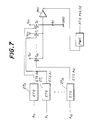
- FIG.7 is a block diagram of the address transition detector.
- the address transition detector is made up of conventional edge trigger circuits 270 - 2710 provided for the respective address bits A0 - A10, p-channel MOS transistors T0 - T10, an inverter INV, a resistor R1 and a pulse width controller PWC.
- the edge trigger circuits 200 - 2710 detect the edges of the corresponding address bits and generates edge trigger signals ETGA ⁇ 0- ETGA10 ⁇ , which are respectively applied to the gates of the transistors T0 - T10.
- the edge trigger signals ETGA0 ⁇ - ETGA10 ⁇ becomes active (low level)
- the corresponding transistor is turned ON, so that a high level is applied to the inverter INV.
- the inverter INV outputs a low level to the pulse width controller PWC, which generates the ATD pulse having a predetermined pulse duration.
- the internal voltage generator 39 is also configured in the same way as the circuit shown in FIG.4A.
- the internal voltage generator 39 generates an internal voltage V INT3 , which is regulated by the aforementioned sense amplifier driving clock ⁇ s generated by the clock generator 18.
- the internal voltage V INT3 is supplied to the sense system 400.
- the internal voltage V INT3 is equal to, for example, 4.0 volts.
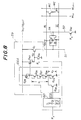
- FIG.8 is a circuit diagram of the internal voltage generator 39 and a part of the sense amplifier and I/O gate 24.
- the internal voltage generator 39 is made up of the aforementioned voltage regulator 100A, a one-shot pulse generator 60, the regulator transistor Q1, two n-channel MOS transistors Q40 and Q41.
- the gate of the regulator transistor Q1 is controlled by the voltage regulator 100A via the transistor Q40.
- the drain of the transistor Q41 is connected to the gate of the regulator transistor Q1, and the source of the transistor Q41 is grounded.
- the source of the regulator transistor Q1 is connected to a high-potential line 51.
- a sense amplifier SA is connected to a pair of bit lines BL and BL ⁇ , to which memory cells MC are connected, as shown in FIG.8.
- the memory cells MC shown in FIG.8 are respectively connected to word lines WL n and WL n+1 .
- the one-shot pulse generator 60 generates a one-shot pulse CLK1 ⁇ in synchronism with the sense amplifier driving signal ⁇ ⁇ s . More specifically, the one-shot pulse CLK1 ⁇ changes to the low level in synchronism with the fall of the sense amplifier driving signal ⁇ ⁇ s .
- the sense amplifier SA is also connected to the high-potential voltage line 51 and a low-potential voltage line 52.
- An n-channel MOS transistor Q42 is provided in the low-potential voltage line 52.
- the sense amplifier driving signals ⁇ s and ⁇ ⁇ s are maintained at the low and high levels, respectively.
- the transistor Q40 and Q41 are turned OFF and ON, respectively, so that the sense amplifier SA is substantially disconnected from the voltage lines 51 and 52.
- the clock signals ⁇ s and ⁇ ⁇ s are reversed, so that the sense amplifier SA starts to operate.
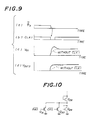
- the sense amplifier driving signal ⁇ ⁇ s changes from the high level to the low level, and as shown in FIG.9-(b), the one-shot pulse CLK1 ⁇ falls.
- the transistor Q30 is turned OFF, so that the gate voltage V G1 increases rapidly, as shown in FIG.9-(c). This rise of the gate voltage V G1 is slightly over-shooting.
- the one-shot pulse CLK1 ⁇ is not provided, the gate voltage V G1 will increase gradually from the ground potential, as illustrated by the broken line in FIG.9-(c).
- the internal voltage V INT3 increases rapidly in response to the rapid increase in the gate voltage V G1 .
- the internal voltage V INT3 will increases gradually if the one-shot pulse CLK1 ⁇ is not provided.
- the transistor Q30 is continuously or intermittently turned OFF, so that the gate voltage V G1 of the regulator transistor Q1 is increased.
- the RAS ⁇ signal is maintained in the high level (inactive state)
- the RAS ⁇ system 200 consumes a small amount of power, so that the transistor Q29 is short-circuited by the transistor Q30.
- the CAS ⁇ system 300 and the sense system 400 are also controlled in the same way as the RAS ⁇ system 200.
- the internal voltage V INT1 supplied to the RAS ⁇ system 200 is controlled separately from the internal voltage V INT2 supplied to the CAS ⁇ system 300.
- an n-channel MOS transistor Q31 is connected in parallel to the transistor Q30. The RAS ⁇ signal is applied to the gate of the transistor Q31, and the CAS ⁇ signal is applied to the gate of the transistor Q30.
- the gate voltage V G1 of the regulator transistor Q1 is increased.
- the refresh operation starts when the CAS signal changes to the low level before the RAS ⁇ signal changes to the low level. If the internal voltage compensation operation starts when the CAS ⁇ signal becomes the low level, the internal voltage will be compensated for excessively because the CAS system 300 does not operate in the CAS ⁇ -before- RAS ⁇ mode. In the configuration shown in FIG.10, when both the CAS ⁇ and RAS ⁇ signals are maintained in the low level, the compensation operation starts.
- the on-chip voltage regulator according to the present invention can be applied to not only DRAMs but also SRAMs.
- SRAMs a chip enable signal CE ⁇ and an output enable signal OE ⁇ are used as the clock signal CLK ⁇ .
- the present invention is suitable for logic LSIs.
Landscapes
- Engineering & Computer Science (AREA)
- Power Engineering (AREA)
- Microelectronics & Electronic Packaging (AREA)
- Physics & Mathematics (AREA)
- Electromagnetism (AREA)
- General Physics & Mathematics (AREA)
- Radar, Positioning & Navigation (AREA)
- Automation & Control Theory (AREA)
- Computer Hardware Design (AREA)
- Dram (AREA)
- Continuous-Control Power Sources That Use Transistors (AREA)
- Semiconductor Integrated Circuits (AREA)
- Semiconductor Memories (AREA)
- Logic Circuits (AREA)
- Static Random-Access Memory (AREA)
Description
- The present invention generally relates to semiconductor integrated circuits, and more particularly to an on-chip voltage regulator for controlling the generation of an internal power supply voltage from an external power supply voltage.
- As the feature scale of LSIs is decreasing, the size of transistors realized by LSIs is reducing, and the breakdown voltages of LSI transistors are decreasing. The are two possible approaches to optimize the relationship between the power supply voltage and the feature scale. The first approach is to produce a transistor having a gate length of approximately 0.8 micrometers which is enough to withstand a high power supply voltage equal to, for example, 5 volts. The second approach is to produce a transistor having a gate length of approximately 0.5 micrometers which is suitable for a decreased power supply voltage equal to, for example, 3.3 volts. It should be noted that the transistor produced by the second approach can operate faster than that produced by the first approach. It is thus concluded that the power supply voltage should be decreased to a suitable voltage as the integration density increases. On the other hand, many IC chips are designed to receive a standardized external power supply voltage equal to 5 volts. Thus, it is necessary to generate a suitably dropped power supply voltage from the standardized external power supply voltage inside of each IC chip.
- FIG.1A is a circuit diagram of a conventional on-chip voltage regulator designed to generate, from an external voltage, an in-chip voltage lower than the external voltage. A regulator transistor Q1 functions as a series control regulator with respect to an external power supply voltage VEXT equal to, for example, 5 volts. The regulator transistor Q1 generates an internal power supply voltage VINT equal to, for example, 3.3 volts from the 5.0V external power supply voltage VEXT. The gate of the regulator transistor Q1 is charged by a voltage obtained by rectifying an A.C. signal generated by a ring oscillator OSC. The gate voltage now labeled VG1 is clamped at a fixed voltage due to the function of a transistor Q4 because the source of the transistor Q4 is set to a reference voltage VREF. The reference voltage VREF can be generated by a conventional method, for example, by using the threshold voltage of a MOS transistor.
- A transistor Q2 functions to charge the gate of the regulator transistor Q1 when the power supply is turned ON. The reference voltage VREF is also applied to the gate of the transistor Q2 and the oscillator OSC. The reference voltage VREF enables the oscillator OSC to generate a fixed oscillation voltage. A capacitor C is connected between the oscillator OSC and the source of the transistor Q2, and functions to increase the charge voltage. For example, when the output voltage of the oscillator OSC is negative, the capacitor C is charged via the transistor Q2 so that the terminal of the C on the side of the transistor Q2 is positive. On the other hand, when the output voltage of the oscillator OSC is positive, the charge voltage is increased so that it becomes equal to the sum of the positive output voltage of the oscillator OSC and the voltage developed across the capacitor C. The oscillator OSC is used for generating the large gate voltage VG1 of the regulator transistor Q1 in order to obtain the stabilized internal voltage VINT. The oscillator OSC may be replaced by an alternative device, which oscillates and rectifies a voltage signal so that a peak voltage can be obtained.
- FIG.1B is a drain current (ID) vs. a gate-source voltage (VGS) of the regulator transistor Q1. The drain current ID can be defined as being ID = k(VG - Vth) where k is a proportional constant, and Vth is the threshold voltage of the regulator transistor Q1. That is, the turn-ON characteristic curve of the regulator transistor Q1 is proportional to the square of the gate-source voltage VGS thereof. If current consumed in the chip varies by ΔI, the internal voltage VINT varies by ΔV. In the case of a DRAM, the current equal to approximately 0.1 mA passes through the regulator transistor Q1 in a standby mode. On the other hand, when an internal circuit of the DRAM is activated, the peak of the current passing through the regulator transistor Q1 becomes approximately equal to 100 mA. That is, the current obtained at the active mode is 1000 times the current obtained in the standby mode. It is possible to increase the gate width to increase the proportional constant k. However, an increase in the gate width decreases the integration density. It can be seen from the above explanation that it is impossible to regulate the internal voltage VINT at the fixed voltage in the state where the current consumed in the internal circuit is varying. Further, an increase in the gate width leads to an increase in a sub-threshold current, and the threshold voltage of the transistor Q1 is greatly decreased. Thus, if a change in the current consumed in the internal chip is equal to 1000 times that obtained in the standby mode, it causes great variations in the internal voltage VINT.
- FIG.1C is another conventional on-chip voltage regulator directed to suppressing variations in the internal voltage VINT. The gate voltage of the regulator transistor Q1 is controlled by an output of a current-mirror type analog differential amplifier, which is composed of transistors Q11 - Q14. That is, a feedback signal is applied to the gate of the transistor Q12 from the source of the transistor Q1, that is, a node from which the internal voltage VINT is output. The reference voltage VREF is applied to the gate of the transistor Q11. Thus, the internal voltage VINT is automatically controlled so that it is always equal to the reference voltage VREF. Thus, the internal voltage VINT is not greatly affected by variations in a load current, that is, the drain current of the transistor Q1.
- Although the voltage stability is good, it is necessary to always pass currents equal to 100 microamperes through the transistors Q11 and Q12 in order to obtain a transfer (amplification) gain necessary for the analog differential amplifier circuit. Thus, a large amount of power is consumed in the circuit shown in FIG.1C in the standby mode. Further, it is necessary to fabricate the circuit so that the feedback circuit can operate stably. If such a requirement is not satisfied, a ringing will occur in the internal voltage VINT. In the worst case, the feedback circuit will oscillate.
- From document US-A-4,649,291 an on-chip voltage regulator for controlling a gate of a regulator transistor is known, the regulator transistor having a first terminal for receiving an external power supply voltage and a second terminal connectable to an internal circuit formed on a chip on which the on-chip voltage regulator is formed. According to this prior art document, the on-chip voltage regulator comprises clock receiving means for receiving a predetermined clock signal related to an operation of the internal circuit as well as regulator means coupled to the clock receiving means and the regulator transistor for generating a gate voltage output to the gate of the regulator transistor on the basis of a state of the predetermined clock signal so that the regulator transistor can generate a substantially fixed internal voltage from the external power supply voltage irrespective of whether or not the internal circuit is operating.
- It is a general object of the present invention to provide a novel and useful on-chip voltage regulator in which the aforementioned disadvantages are eliminated.
- A more specific object of the present invention is to provide an on-chip voltage regulator capable of generating an internal voltage little affected by variations in the load current and consuming a small amount of current in the standby mode.
- According to the invention, the above-mentioned objects are achieved by an on-chip voltage regulator for controlling a gate of a regulator transistor having a first terminal connectable to receive an external power supply voltage and a second terminal connectable to an internal circuit formed on a chip on which the on-chip voltage regulator is formed, the on-chip regulator comprising clock receiving means for receiving a predetermined clock signal related to an operation of the internal circuit, and regulator means coupled to the clock receiving means and the regulator transistor for generating a gate voltage output to the gate of the regulator transistor on the basis of a state of the predetermined clock signal so that the regulator transistor can generate a substantially fixed internal voltage from the external power supply voltage irrespective of whether or not the internal circuit is operating, wherein a capacitance is added to the gate of the regulator transistor and the gate potential of the regulator transistor is controlled on the basis of the active period of the clock or its frequency.
- Other objects, features and advantages of the present invention will become more apparent from the following detailed description when read in conjunction with the accompanying drawings, in which:
- FIG.1A is a circuit diagram of a conventional internal voltage regulator;
- FIG.1B is a graph illustrating a drain current vs. gate-source voltage characteristic of a regulator transistor shown in FIG.lA;
- FIG.1C is a circuit diagram of another conventional internal voltage regulator;
- FIG.2 is a circuit diagram of an on-chip voltage regulator according to a first preferred embodiment of the present invention;
- FIG.3 is a waveform diagram illustrating the operation of the voltage regulator shown in FIG.2;
- FIG.4A is a circuit diagram of an on-chip voltage regulator according to a second preferred embodiment of the present invention;
- FIG.4B is a cross-sectional view of a semiconductor layer structure which realizes some transistors shown in FIG.4A;
- FIG.4C is a cross-sectional view of a variation of the layer structure shown in FIG.4B;
- FIG.5 is a circuit diagram of a variation of the on-chip voltage regulator shown in FIG.2;
- FIG.6 is a DRAM device having the on-chip voltage regulator according the present invention;
- FIG.7 is a circuit diagram of an address transition detector provided in the DRAM shown in FIG.6;
- FIG.8 is a circuit diagram of an internal voltage generator shown in FIG.6;
- FIG.9 is a waveform diagram illustrating the operation of the circuit shown in FIG.8; and
- FIG.10 is a circuit diagram of a variation of the internal voltage generator shown in FIG.6.
- Referring to FIG.2, an on-
chip voltage regulator 100 controls the regulator transistor Q1. Thevoltage regulator 100 has an input terminal receiving a clock signal
voltage regulator 100 is composed of a constant-current source I, diode-connected n-channel MOS transistors Q26, Q27, Q28 and Q29 connected in series, an n-channel MOS transistor Q30, and a capacitor C. - The constant-current source I, and the transistors Q26 - Q29 are connected in series and provided between a positive internal voltage line having a voltage VA and ground. The gate of each of the transistors Q26 - Q29 is connected to the drain thereof. The transistors Q30 is connected in parallel to the transistor Q29. A low-active clock signal


- Assuming that each of the transistors Q26 - Q29 has an identical threshold voltage Vth, V1 = 3Vth, and V2 = Vth where V1 is a voltage developed across the series connected transistors Q26 - Q28, and V2 is a voltage developed across the transistor Q29. When the clock signal


- The load L (corresponding to an internal circuit) on a chip on which the voltage regulator is also formed is maintained in the standby mode, the low-active clock signal


- As shown in FIG.3, the clock signal


However, according to the conventional voltage regulator shown in FIG.1A or FIG.1C, the internal voltage VINT is continuously decreasing even after time t₂, as depicted by a broken line C2 in FIG.3. This means that a large variation in the internal voltage VINT occurs. If the transistor Q30 is omitted, the internal voltage VINT will be decreasing continuously after time t₂. According to the embodiment of the present invention, each time the transistor Q30 is turned OFF, the voltage V2 equal to the threshold voltage Vth of the transistor Q29 is added to the voltage V1, so that the gate voltage VG1 of the regulator transistor Q1 is increased. - During the time when the clock signal


- When the clock signal

- As has been described above, the internal resistance of the regulator transistor Q1 is controlled on the basis of the ON/OFF frequency (or the activated period) of the clock signal

- As has been described above, the internal resistance of the regulator transistor Q1 is changed so that the voltage drop obtained when a small amount of current passes through the internal circuit is substantially equal to the voltage drop obtained when a large amount of current passes through the internal circuit. Generally, the load L includes a capacitor of a circuit element and/or a parasitic capacitor. The internal voltage VINT is associated with the charging and discharging of such a capacitor. Thus, a variation takes place slowly. When the clock signal

- A description will now be given of a second preferred embodiment of the present invention with reference to FIGS.4A and 4B, in which those parts which are the same as those shown in FIG.3 are given the same reference numerals. An on-
chip voltage regulator 100A according to the second preferred embodiment includes the constant-current source I which is formed of a depletion type n-channel MOS transistor in which its gate and source are short-circuited. The regulator transistor Q1 is also formed of a depletion type n-channel MOS transistor in which its gate and source are short-circuited. The circuit is designed to pass a large amount of current through the regulator transistor Q1 in a five-tube characteristic region. Such an operation results in a substrate current. - FIG.4B shows the cross section of a semiconductor chip which realizes the transistor Q1 or Q25 shown in FIG.4A. As shown, the transistor is formed in a p-
type silicon substrate 1, which is biased by a substrate bias voltage VBB (or VSS) which is generated in the chip. The substrate current flows into a VBB generation circuit (which corresponds to a substrate bias generator, as will be described later), and causes the VBB generation circuit to operate unstably. In order to overcome this problem, an n-type well 2 is formed in the p-type substrate 1, and a p-type well 3 is formed in the n-type well 2. The p-type well 3 is electrically connected to a source region S. With this arrangement, the substrate current generated by the regulator transistor Q1 overlaps with the output current of the regulator transistor Q1, and thus the problem arising from the substrate current is eliminated. - The transistor Q25 can be fabricated in the same way as the regulator transistor Q1. However, the reason why the transistor Q25 is formed in the p-type well in the n-type well is different from the above-mentioned reason regarding the regulator transistor Q1. The transistor Q25 functions as a constant-current source by connecting the gate to the source. Since the constant-current output of the transistor Q25 is output from the source thereof, a change in the source voltage causes a change in a backgate voltage (which corresponds to the potential difference between the source of the transistor Q25 and the potential of the p-
type substrate 1 which is the back gate), if the transistor Q25 is directly formed in the p-type substrate 1. Thus, a so-called substrate bias effect appears and deteriorates the constant-current characteristic of the transistor Q25. The substrate bias effect is such that as the back gate bias increases, the threshold voltage Vth of the transistor Q25 increases and thus the drain current decreases. - On the other hand, the layer structure shown in FIG.4B is formed so that the back gate is the p-type well 3 in the n-
type well 2, and the p-type well 3 is connected to thesource 5. Thereby, when the source voltage changes, the back gate voltage also changes, so that the occurrence of a change in the drain current arising from the substrate bias effect can be suppressed. As a result, a good constant-current characteristic can be obtained. - The transistor Q25 is formed of a depletion type MOS transistor, and thus it is not necessary to provide the aforementioned voltage VA higher than the standard external power supply voltage VEXT, as shown in FIG.2. It is necessary to generate the voltage VA higher than the power supply voltage VEXT inside of the chip. Such a VA generation circuit consumes some power. Thus, it is preferable to use the configuration shown in FIG.4A in most cases.
- FIG.4C shows the cross section of an alternative layer structure designed to preventing the occurrence of the aforementioned substrate bias effect. In order to make the back gate voltage set equal to the source voltage, a transistor is formed in a p-type well 5 formed in an n-
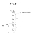
type silicon substrate 4, and the p-type well 5 is electrically connected to the source S. - The circuit structure for generating and oscillating the gate voltage VG1 of the regulator transistor Q1 is not limited to the aforementioned circuit structure. As shown in FIG.5, m transistors (m is an integer equal to or larger than 1) and n transistors (n is an integer equal to or larger than 1) are connected in series. When the clock signal

- A description will now be given of a semiconductor memory device which uses the above-mentioned on-chip voltage regulator. FIG.6 shows a DRAM device, which includes a

system 200, a
system 300, asense system 400 and an internalvoltage generation circuit 500. The
system 200 operates in accordance with a row address strobe signal


system 300 operates in accordance with a column address strobe signal

sense system 300 operates in accordance with a pair of sense amplifier driving clocks φs and φs. The internalvoltage generation circuit 500 includes threeinternal voltage generator - The

system 200 includes apredecoder 12a, apredecoder 12b, a row address decoder 16, aclock generator 18, amode controller 32 and arefresh address counter 34. The
system 300 includes theaddress buffer 12a, thepredecoder 12b, acolumn address decoder 14, a clock generator 22, awrite clock generator 26 and adata input buffer 28. Thesense system 300 includes a memory cell array 10, and a sense amplifier/input output gate 24. - The memory cell array 10 has a plurality of memory cells arranged into rows and columns and coupled to word lines and bit lines.
- A multiplexed address signal ADD consisting of address bits A₀ to A₁₀ is input to the
address buffer 12a, which outputs a column address signal to thecolumn address decoder 14. The address signal ADD is also supplied to thepredecoder 12b, which outputs a row address signal to the row address decoder 16. The row address strobe signal
clock generator 18, which generates a clock signal supplied to the row address decoder 16. The row address strobe signal
output gate 24 is connected to thecolumn address decoder 14 and the memory cell array 10. - The column address strobe signal

gate 20 through an inverter. The clock signal output by theclock generator 18 is applied to the ANDgate 20, an output signal of which is input to the clock generator 22. In response to the column address strobe signal
column address decoder 14 as well as theaddress buffer 12a. When receiving the clock signal from the clock generator 22, thecolumn address decoder 14 selects a corresponding one of pairs of bit lines or more. The sense amplifier and input/output gate 24 is coupled to the bit lines running in the memory cell array 10. When writing data Din into the memory cell array 10 or reading out data Dout therefrom, the data is amplified by a sense amplifier provided in the sense amplifier and input/output gate 24. - The
write clock generator 26 receives the clock signal from the clock generator 22 and a write enable signal
data input buffer 28 inputs data Din at a timing defined by the write clock supplied from thewrite clock generator 26. Data output from thedata input buffer 28 is input to the sense amplifier and input/output gate 24 and is written into the memory cell array 10. Data output from the sense amplifier and input/output gate 24 is input to adata output buffer 30, which outputs the input data in synchronism with the clock signal from the clock generator 22. Themode controller 32 receives the column address strobe signal
clock generator 18, and generates a mode signal corresponding to predetermined conventional operation modes, such as a read/write mode, a read modified write mode and a

mode controller 32 is input to therefresh address counter 34, which generates an address signal showing a memory cell to be refreshed. Asubstrate bias generator 36 generates a substrate bias voltage, such as the aforementioned voltage VBB. - The
internal voltage generator 37 of the internalvoltage generation circuit 500 is configured according to the present invention. For example, theinternal voltage generator 37 has the structure shown in FIG.4A. Theinternal voltage generator 37 generates an internal voltage VINT1, which is regulated by the


system 200. The external power supply voltage VEXT is equal to 5 volts (Vcc), and the internal voltage VINT1 is equal to, for example, 3.3 volts. - The
internal voltage generator 38 is also configured in the same way as the circuit shown in FIG.4A. Theinternal voltage generator 38 generates an internal voltage VINT2, which is regulated by an address transition detection signal ATD, which is input, as the clock signal

system 300. The internal voltage VINT2 is equal to, for example, 3.3 volts. - The address transition signal ATD is generated when a change in the address signal ADD is detected. An address transition detector is provided in, for example, the block of the
address buffer 12a. - FIG.7 is a block diagram of the address transition detector. As shown, the address transition detector is made up of conventional edge trigger circuits 27₀ - 27₁₀ provided for the respective address bits A₀ - A₁₀, p-channel MOS transistors T₀ - T₁₀, an inverter INV, a resistor R1 and a pulse width controller PWC. The edge trigger circuits 20₀ - 27₁₀ detect the edges of the corresponding address bits and generates edge trigger signals


- Turning now to FIG.6, the
internal voltage generator 39 is also configured in the same way as the circuit shown in FIG.4A. Theinternal voltage generator 39 generates an internal voltage VINT3, which is regulated by the aforementioned sense amplifier driving clock φs generated by theclock generator 18. The internal voltage VINT3 is supplied to thesense system 400. The internal voltage VINT3 is equal to, for example, 4.0 volts. - FIG.8 is a circuit diagram of the
internal voltage generator 39 and a part of the sense amplifier and I/O gate 24. Theinternal voltage generator 39 is made up of theaforementioned voltage regulator 100A, a one-shot pulse generator 60, the regulator transistor Q1, two n-channel MOS transistors Q40 and Q41. The gate of the regulator transistor Q1 is controlled by thevoltage regulator 100A via the transistor Q40. The drain of the transistor Q41 is connected to the gate of the regulator transistor Q1, and the source of the transistor Q41 is grounded. The source of the regulator transistor Q1 is connected to a high-potential line 51. A sense amplifier SA is connected to a pair of bit lines BL and


- The sense amplifier SA is also connected to the high-
potential voltage line 51 and a low-potential voltage line 52. An n-channel MOS transistor Q42 is provided in the low-potential voltage line 52. During the time when the sense amplifier SA is maintained in the inactive state, the sense amplifier driving signals φs and
voltage lines 
- At this time, as shown in FIG.9-(a), the sense amplifier driving signal


- In can been from the above description, that the state where the sense amplifier SA starts to operate is detected from the sense amplifier driving signal


- As has been described above, during the time when the


system 200 starts to operate. On the other hand, the

system 200 consumes a small amount of power, so that the transistor Q29 is short-circuited by the transistor Q30. The
system 300 and thesense system 400 are also controlled in the same way as the
system 200. - In the structure shown in FIG.6, the internal voltage VINT1 supplied to the

system 200 is controlled separately from the internal voltage VINT2 supplied to the
system 300. Alternatively, as shown in FIG.10, it is possible to regulate the internal voltages VINT1 and VINT2 on the basis of a composite logic of the


CAS system 300 does not operate in the


- The on-chip voltage regulator according to the present invention can be applied to not only DRAMs but also SRAMs. In the SRAMs, a chip enable signal


Claims (27)
- An on-chip voltage regulator for controlling a gate of a regulator transistor (Q1) having a first terminal connectable to receive an external power supply voltage (VEXT) and a second terminal connectable to an internal circuit formed on a chip on which said on-chip voltage regulator is formed, whereby said on-chip voltage regulator comprises:clock receiving means (a30) for receiving a predetermined clock signal (

 regulator means (I, Q26 - Q30, Q31), coupled to said clock receiving means and said regulator transistor, for generating a gate voltage (VG1) output to the gate of said regulator transistor on the basis of a state of said predetermined clock signal so that said regulator transistor can generate a substantially fixed internal voltage (VINT) from said external power supply voltage irrespective of whether or not said internal circuit is operatingcharacterized in thata capacitance (C) is added to the gate of said regulator transistor (Q1), andin that the gate potential of the regulator transistor (Q1) is controlled on the basis of the active period of the clock or its frequency.
 - An on-chip voltage regulator as claimed in claim 1, characterized in that said regulator means comprises means (I, Q26 - Q30) for outputting a first gate voltage (V1) supplied to the gate of said regulator transistor when said predetermined clock signal is maintained at a first state and for generating a second gate voltage (V1 + V2) supplied to the gate of said regulator transistor when said predetermined clock signal is maintained at a second state.
- An on-chip voltage regulator as claimed in claim 1, characterized in that said voltage regulator comprises means (I, Q26 - Q30) for increasing said gate voltage output to the gate of said regulator transistor when said predetermined clock signal changes from a first state indicating that said internal circuit is maintained in a standby mode to a second state indicating said internal circuit is operating.
- An on-chip voltage regulator as claimed in claim 1, characterized in that said on-chip voltage regulator further comprises pulse generating means (60) for generating said predetermined clock signal from a state indicating signal indicating whether or not said internal circuit is operating.
- An on-chip voltage regulator as claimed in claim 4, characterized in that said pulse generating means generates a one-shot pulse (

- An on-chip voltage regulator as claimed in claim 1, characterized in that said on-chip voltage regulator comprises pulse generating means (Q30, Q31) for receiving a plurality of state indicating signals (


- An on-chip voltage regulator as claimed in claim 1, characterized in that said regulator means comprises:a constant-current source (I) connectable to receive a first predetermined power supply voltage (VA, VEXT);first voltage generating means (Q26 - Q28), connected to said constant-current source in series and connected to the gate of said regulator transistor, for generating a first voltage (V1) from a constant current generated by said constant-current source;second voltage generating means (Q29), connected to said first voltage generating means in series and connectable to receive a second predetermined power supply voltage (ground level) lower than said first predetermined voltage, for generating a second voltage (V2) from said constant current supplied from said constant-current source through said first voltage generating means; andcontrol means (Q30), coupled to said second voltage generating means, for selectively short-circuiting said second voltage generating means on the basis of the state of said predetermined clock signal so that either a voltage equal to the sum (V1 + V2) of said first voltage and second voltage or said first voltage (V1) is selectively output, as said gate voltage, to the gate of said regulator transistor.
- An on-chip voltage regulator as claimed in claim 7, characterized in that:said first voltage generating means comprises m field effect transistors (Q26 - Q28) where m is an integer equal to or larger than 1;said m field effect transistors are diode-connected and connected in series; andsaid first voltage substantially corresponds to the sum of threshold voltages of said m field effect transistors.
- An on-chip voltage regulator as claimed in claim 7, characterized in that:said second voltage generating means comprises n field effect transistors (Q29) where n is an integer equal to or larger than 1;said n field effect transistors are diode-connected and connected in series; andsaid second voltage substantially corresponds to the sum of threshold voltages of said n field effect transistors.
- An on-chip voltage regulator as claimed in claim 7, characterized in that said control means comprises a transistor (Q30) having a control terminal connectable to receive said predetermined clock signal (


- An on-chip voltage regulator as claimed in claim 7, characterized in that:said constant-current source comprises a field effect transistor (Q25) of a depletion type; andsaid field effect transistor of said constant-current source comprises a gate terminal, a first terminal connectable to receive said first predetermined power supply voltage, and a second terminal connected to said gate terminal and the gate of said regulator transistor.
- An on-chip voltage regulator as claimed in claim 11, characterized in that said field effect transistor comprises:a substrate (1) having a first conductivity type;a first well (2) formed in said substrate and having a second conductivity type opposite to said first conductivity type;a second well (3) formed in said first well and having the first conductivity type;a first diffusion region (S) formed in said second well and having the second conductivity type, said first diffusion region corresponding to said first terminal;a second diffusion region (D) formed in said second well and having the second conductivity type, said second diffusion region corresponding to said second terminal; anda gate (G) positioned between said first and second diffusion regions, said gate corresponding to said gate terminal.
- An on-chip voltage regulator as claimed in claim 12, characterized in that said first well is connectable to receive said external power supply voltage (VEXT).
- An on-chip voltage regulator as claimed in claim 11, characterized in that said first predetermined power supply voltage is equal to said external power supply voltage.
- An on-chip voltage regulator as claimed in claim 11, characterized in that said field effect transistor comprises:a substrate (4) having a first conductivity type;a well (5) formed in said substrate and having a second conductivity type opposite to said first conductivity type;a first diffusion region (S) formed in said well and having the first conductivity type, said first diffusion region corresponding to said first terminal;a second diffusion region (D) formed in said well and having the first conductivity type, said second diffusion region corresponding to said second terminal; anda gate (G) positioned between said first and second diffusion regions, said gate corresponding to said gate terminal.
- An on-chip voltage regulator as claimed in claim 15, characterized in that said first well is connectable to receive said external power supply voltage.
- An on-chip voltage regulator as claimed in claim 7, characterized in that said on-chip voltage regulator comprises a capacitor having a first terminal coupled to the gate of said regulator transistor, and a second terminal connectable to receive said reference voltage.
- An on-chip voltage regulator as claimed in claim 1, characterized in that said regulator means comprises means (Q26 - Q30) for changing an internal resistance of said regulator transistor on the basis of the state of said predetermined clock.
- An on-chip voltage regulator as claimed in claim 1, characterized in that said regulator means comprises:constant-current generation means (I) for generating a constant current; andvariable resistance means (Q29 - Q30), coupled to said constant-current generation means and said regulator transistor, for providing a variable resistance dependent on the state of said predetermined clock and for outputting a voltage (V1. V1 + V2) obtained by passing said constant current through said variable resistance means to the gate of said regulator transistor.
- An on-chip voltage regulator as claimed in claim 1 characterized in that said regulator is comprized in an internal voltage generating means and in that said internal circuit isa semiconductor memory device comprising:a first system (300) operating in accordance with a first clock signal (φs,
 a second system (200) operating in accordance with a second clock signal (RAS) and having row address means (12a, 12b, 16) for generating a row address from an external address and for outputting said row address to said memory cell array; anda third system operating in accordance with a third clock signal (ATD,
 whereby said internal voltage generating means (500) is coupled to said first, second and third systems, for generating first, second and third internal voltages (VINT1, VINT2, VINT3) from saidexternal power supply voltage (VEXT) on the basis of states of said first, second and third clock signals and for outputting said first, second and third internal voltages to said first, second and third systems, respectively, andsaid internal voltage generating means is provided witha regulator transistor (Q1) for each of said first, second and third systems and having a first terminal connectable to receive said external power supply voltage and a second terminal connected to a corresponding one of said first, second and third systems; andregulator means, connected to each of said regulator transistors for generating a gate voltage (VG1) output to the gate of said regulator transistor on the basis of the state of at least one of said first, second and third clock signals so that a corresponding one of said first, second and third internal voltages is substantially fixed irrespective of whether or not said corresponding one of the first, second and third systems is operating.
 - An on-chip voltage regulator as claimed in claim 20, characterized in that:said regulator means comprises means (39) for controlling the gate voltage output to the gate of said regulator transistor provided for said first system on the basis of the state of said first clock signal; andsaid first clock signal is synchronized with a sense amplifier driving signal (φs,

- An on-chip voltage regulator as claimed in claim 21, characterized by further comprising pulse generating means (60) for generating a one-shot pulse (

- An on-chip voltage regulator as claimed in claim 20, characterized in that:said regulator means comprises means (38) for generating the gate voltage output to the gate of said regulator transistor provided for said second system on the basis of the state of said second clock signal; andsaid second clock signal is a row address strobe signal supplied from an external device.
- An on-chip voltage regulator as claimed in claim 20, characterized in that:said regulator means comprises means (39) for generating the gate voltage output to the gate of said regulator transistor provided for said second system on the basis of the state of said second clock signal; andsaid semiconductor memory device comprises address transition detection means (27₀- 27₁₀, T₀ - T₁₀, R1, INV, PWC) for detecting a change in said external address and for outputting a pulse signal (ATD) when the change in said external address is detected, said pulse signal corresponding to said second clock signal.
- An on-chip voltage regulator as claimed in claim 20, characterized in that said regulator means comprises means (Q26 - Q31) for generating the gate voltage output to the gate of said regulator transistor provided for each of said second and third systems on the basis of the states of said second and third clock signals (


- An on-chip voltage regulator (Q1) according to claim 1 characterized in that said regulator is comprised in a semiconductor integrated circuit deviceand in that said semiconductor integrated circuit device comprises means (100, 100A), coupled to said on-chip voltage control circuit, for controlling a current supply ability of said on-chip voltage regulator so that said current supply ability obtained when said internal circuit is maintained in an active state is greater than said current supply ability obtained when said internal circuit is maintained in an inactive state.
- An on-chip voltage regulator according to claim 26characterized in that said means (100, 100A) are coupled to the gate of said regulator transistor of said on-chip voltage regulator, for changing an internal resistance of said regulator transistor in accordance with the clock which controls active/inactive states of said internal circuit of said semiconductor integrated circuit device to thereby suppress a difference between the internal power supply voltage obtained when the internal circuit is maintained in the active state and the internal power supply voltage obtained when the internal circuit is maintained in the inactive state.
Applications Claiming Priority (2)
| Application Number | Priority Date | Filing Date | Title |
|---|---|---|---|
| JP8376090 | 1990-03-30 | ||
| JP83760/90 | 1990-03-30 |
Publications (3)
| Publication Number | Publication Date |
|---|---|
| EP0449310A2 EP0449310A2 (en) | 1991-10-02 |
| EP0449310A3 EP0449310A3 (en) | 1992-02-05 |
| EP0449310B1 true EP0449310B1 (en) | 1996-03-13 |
Family
ID=13811526
Family Applications (1)
| Application Number | Title | Priority Date | Filing Date |
|---|---|---|---|
| EP91105071A Expired - Lifetime EP0449310B1 (en) | 1990-03-30 | 1991-03-28 | On-chip voltage regulator and semiconductor memory device using the same |
Country Status (5)
| Country | Link |
|---|---|
| US (1) | US5097303A (en) |
| EP (1) | EP0449310B1 (en) |
| JP (1) | JP3124781B2 (en) |
| KR (1) | KR940009835B1 (en) |
| DE (1) | DE69117784T2 (en) |
Families Citing this family (34)
| Publication number | Priority date | Publication date | Assignee | Title |
|---|---|---|---|---|
| JP3068291B2 (en) * | 1990-12-12 | 2000-07-24 | 新日本製鐵株式会社 | Semiconductor storage device |
| JPH04333277A (en) * | 1991-05-09 | 1992-11-20 | Nec Ic Microcomput Syst Ltd | Semiconductor memory device |
| US5253205A (en) * | 1991-09-05 | 1993-10-12 | Nippon Steel Semiconductor Corporation | Bit line and cell plate clamp circuit for a DRAM |
| JPH06236686A (en) * | 1993-01-22 | 1994-08-23 | Nec Corp | Semiconductor device |
| US5515319A (en) * | 1993-10-12 | 1996-05-07 | Texas Instruments Incorporated | Non-volatile memory cell and level shifter |
| EP0661717B1 (en) * | 1993-12-31 | 2000-03-29 | STMicroelectronics S.r.l. | Voltage regulator for programming non-volatile and electrically programmable memory cells |
| US5786720A (en) * | 1994-09-22 | 1998-07-28 | Lsi Logic Corporation | 5 volt CMOS driver circuit for driving 3.3 volt line |
| US5721485A (en) * | 1996-01-04 | 1998-02-24 | Ibm Corporation | High performance on-chip voltage regulator designs |
| US5663919A (en) * | 1996-02-28 | 1997-09-02 | Micron Technology, Inc. | Memory device with regulated power supply control |
| US5999039A (en) * | 1996-09-30 | 1999-12-07 | Advanced Micro Devices, Inc. | Active power supply filter |
| JP3963990B2 (en) * | 1997-01-07 | 2007-08-22 | 株式会社ルネサステクノロジ | Internal power supply voltage generation circuit |
| US5818291A (en) * | 1997-04-04 | 1998-10-06 | United Memories, Inc. | Fast voltage regulation without overshoot |
| US7467379B2 (en) * | 2001-01-16 | 2008-12-16 | International Business Machines Corporation | System and method for incrementally executing a client/server application |
| US20030122173A1 (en) * | 2001-12-28 | 2003-07-03 | Rabadam Eleanor P. | Package for a non-volatile memory device including integrated passive devices and method for making the same |
| US6498737B1 (en) * | 2002-01-16 | 2002-12-24 | Taiwan Semiconductor Manufacturing Company | Voltage regulator with low sensitivity to body effect |
| US6850856B1 (en) * | 2002-11-18 | 2005-02-01 | Sun Microsystems, Inc. | I/O receiver thermal correction scheme |
| US7554312B2 (en) * | 2003-06-30 | 2009-06-30 | Intel Corporation | DC-to-DC voltage converter |
| US6924692B2 (en) * | 2003-06-30 | 2005-08-02 | Intel Corporation | Voltage reference generator |
| US7170308B1 (en) * | 2003-07-28 | 2007-01-30 | Altera Corporation | On-chip voltage regulator using feedback on process/product parameters |
| US7119604B2 (en) * | 2004-06-17 | 2006-10-10 | Taiwan Semiconductor Manufacturing Company, Ltd. | Back-bias voltage regulator having temperature and process variation compensation and related method of regulating a back-bias voltage |
| US7151697B2 (en) * | 2004-11-30 | 2006-12-19 | Infineon Technologies Ag | Non-volatile semiconductor memory |
| JP4761833B2 (en) * | 2005-05-24 | 2011-08-31 | 株式会社東芝 | Semiconductor device and system |
| US8624636B2 (en) * | 2006-05-22 | 2014-01-07 | Brillouin Energy Corp. | Drive circuit and method for semiconductor devices |
| US20070268045A1 (en) * | 2006-05-22 | 2007-11-22 | Profusion Energy, Inc. | Drive Circuit And Method For Semiconductor Devices |
| JP4960179B2 (en) * | 2007-08-28 | 2012-06-27 | ルネサスエレクトロニクス株式会社 | Data processing apparatus, power supply voltage generation circuit, and power supply voltage generation method thereof |
| US7919840B2 (en) * | 2007-11-20 | 2011-04-05 | International Business Machines Corporation | Integrated non-isolated VRM and microprocessor assembly |
| US7705685B2 (en) * | 2007-12-06 | 2010-04-27 | Hong Kong Applied Science And Technology Research Institute Co., Ltd. | Low-voltage oscillator with capacitor-ratio selectable duty cycle |
| JP2009164415A (en) * | 2008-01-08 | 2009-07-23 | Mitsumi Electric Co Ltd | Semiconductor device |
| JP2010157277A (en) * | 2008-12-26 | 2010-07-15 | Toshiba Corp | Nonvolatile semiconductor memory device |
| JP5593904B2 (en) * | 2010-07-16 | 2014-09-24 | 株式会社リコー | Voltage clamp circuit and integrated circuit using the same |
| EP3295310A4 (en) * | 2015-05-14 | 2018-12-26 | Adesto Technologies Corporation | Concurrent read and reconfigured write operations in a memory device |
| JP1643024S (en) * | 2019-03-15 | 2019-10-07 | ||
| DE112021001123T5 (en) * | 2020-02-19 | 2022-12-22 | Rohm Co., Ltd. | parenthesis |
| US11955196B2 (en) * | 2022-07-13 | 2024-04-09 | Nanya Technology Corporation | Memory device, voltage generating device and voltage generating method thereof |
Family Cites Families (12)
| Publication number | Priority date | Publication date | Assignee | Title |
|---|---|---|---|---|
| JPS5780828A (en) * | 1980-11-07 | 1982-05-20 | Hitachi Ltd | Semiconductor integrated circuit device |
| JPS58105563A (en) * | 1981-12-17 | 1983-06-23 | Mitsubishi Electric Corp | Substrate bias generating circuit |
| US4491938A (en) * | 1981-12-28 | 1985-01-01 | Texas Instruments Incorporated | Low voltage RAM cell |
| JPS59218042A (en) * | 1983-05-26 | 1984-12-08 | Toshiba Corp | Semiconductor integrated circuit |
| JPS60176121A (en) * | 1984-02-22 | 1985-09-10 | Toshiba Corp | Voltage drop circuit |
| JPS60179998A (en) * | 1984-02-28 | 1985-09-13 | Fujitsu Ltd | Voltage detecting circuit |
| JPS6199363A (en) * | 1984-10-19 | 1986-05-17 | Mitsubishi Electric Corp | Substrate-potential generating circuit |
| US4698789A (en) * | 1984-11-30 | 1987-10-06 | Kabushiki Kaisha Toshiba | MOS semiconductor device |
| JPS61163655A (en) * | 1985-01-14 | 1986-07-24 | Toshiba Corp | Complementary type semiconductor integrated circuit |
| JPS6273489A (en) * | 1985-09-25 | 1987-04-04 | Mitsubishi Electric Corp | Nonvolatile semiconductor memory device |
| US4973922A (en) * | 1987-11-27 | 1990-11-27 | At&T Bell Laboratories | Voltage controlled variable capacitor and oscillator using it |
| US5046052A (en) * | 1988-06-01 | 1991-09-03 | Sony Corporation | Internal low voltage transformation circuit of static random access memory |
-
1991
- 1991-03-19 JP JP03055150A patent/JP3124781B2/en not_active Expired - Lifetime
- 1991-03-28 DE DE69117784T patent/DE69117784T2/en not_active Expired - Fee Related
- 1991-03-28 EP EP91105071A patent/EP0449310B1/en not_active Expired - Lifetime
- 1991-03-29 US US07/677,560 patent/US5097303A/en not_active Expired - Lifetime
- 1991-03-30 KR KR1019910005205A patent/KR940009835B1/en not_active IP Right Cessation
Also Published As
| Publication number | Publication date |
|---|---|
| US5097303A (en) | 1992-03-17 |
| KR910017630A (en) | 1991-11-05 |
| EP0449310A2 (en) | 1991-10-02 |
| KR940009835B1 (en) | 1994-10-17 |
| JP3124781B2 (en) | 2001-01-15 |
| EP0449310A3 (en) | 1992-02-05 |
| DE69117784D1 (en) | 1996-04-18 |
| DE69117784T2 (en) | 1996-10-24 |
| JPH04212782A (en) | 1992-08-04 |
Similar Documents
| Publication | Publication Date | Title |
|---|---|---|
| EP0449310B1 (en) | On-chip voltage regulator and semiconductor memory device using the same | |
| US6492863B2 (en) | Internal high voltage generation circuit capable of stably generating internal high voltage and circuit element therefor | |
| JP3510335B2 (en) | Semiconductor memory device, internal power supply voltage generation circuit, internal high voltage generation circuit, intermediate voltage generation circuit, constant current source, and reference voltage generation circuit | |
| KR940001640B1 (en) | Semiconductor integrated circuit device | |
| US6597236B1 (en) | Potential detecting circuit for determining whether a detected potential has reached a prescribed level | |
| KR100236816B1 (en) | Semiconductor memory device with reduced leak current | |
| US5442277A (en) | Internal power supply circuit for generating internal power supply potential by lowering external power supply potential | |
| US6535435B2 (en) | Reference voltage generator permitting stable operation | |
| US6954103B2 (en) | Semiconductor device having internal voltage generated stably | |
| JP4353621B2 (en) | Semiconductor device | |
| KR20030037266A (en) | Inner voltage level control circuit, semiconductor storage, and method for controlling them | |
| JP2003068079A (en) | Semiconductor memory | |
| US6121812A (en) | Delay circuit having delay time free from influence of operation environment | |
| KR100331549B1 (en) | Current Sense Amplifier Circuit using Dummy Bit Line | |
| CN111833923A (en) | System and apparatus for discharging leakage current | |
| US5774405A (en) | Dynamic random access memory having an internal circuit using a boosted potential | |
| US6330173B1 (en) | Semiconductor integrated circuit comprising step-up voltage generation circuit | |
| KR19990029191A (en) | Semiconductor integrated circuit device with improved low voltage operation | |
| US6614270B2 (en) | Potential detecting circuit having wide operating margin and semiconductor device including the same | |
| US5875145A (en) | Semiconductor memory device having a voltage lowering circuit of which supplying capability increases when column system is in operation | |
| US4875195A (en) | Semiconductor device with a reference voltage generator | |
| US5990729A (en) | Semiconductor integrated circuit having first and second voltage step down circuits | |
| US9001610B2 (en) | Semiconductor device generating internal voltage | |
| JPH0695752A (en) | Semiconductor integrated circuit | |
| KR930008314B1 (en) | Static voltage generating circuit of semiconductor memory device |
Legal Events
| Date | Code | Title | Description |
|---|---|---|---|
| PUAI | Public reference made under article 153(3) epc to a published international application that has entered the european phase |
Free format text: ORIGINAL CODE: 0009012 |
|
| AK | Designated contracting states |
Kind code of ref document: A2 Designated state(s): DE FR GB IT |
|
| PUAL | Search report despatched |
Free format text: ORIGINAL CODE: 0009013 |
|
| AK | Designated contracting states |
Kind code of ref document: A3 Designated state(s): DE FR GB IT |
|
| 17P | Request for examination filed |
Effective date: 19920728 |
|
| 17Q | First examination report despatched |
Effective date: 19940511 |
|
| GRAH | Despatch of communication of intention to grant a patent |
Free format text: ORIGINAL CODE: EPIDOS IGRA |
|
| GRAA | (expected) grant |
Free format text: ORIGINAL CODE: 0009210 |
|
| AK | Designated contracting states |
Kind code of ref document: B1 Designated state(s): DE FR GB IT |
|
| PG25 | Lapsed in a contracting state [announced via postgrant information from national office to epo] |
Ref country code: FR Effective date: 19960313 |
|
| REF | Corresponds to: |
Ref document number: 69117784 Country of ref document: DE Date of ref document: 19960418 |
|
| ITF | It: translation for a ep patent filed | ||
| EN | Fr: translation not filed | ||
| PLBE | No opposition filed within time limit |
Free format text: ORIGINAL CODE: 0009261 |
|
| STAA | Information on the status of an ep patent application or granted ep patent |
Free format text: STATUS: NO OPPOSITION FILED WITHIN TIME LIMIT |
|
| 26N | No opposition filed | ||
| REG | Reference to a national code |
Ref country code: GB Ref legal event code: IF02 |
|
| REG | Reference to a national code |
Ref country code: GB Ref legal event code: 732E |
|
| PGFP | Annual fee paid to national office [announced via postgrant information from national office to epo] |
Ref country code: GB Payment date: 20090325 Year of fee payment: 19 |
|
| PGFP | Annual fee paid to national office [announced via postgrant information from national office to epo] |
Ref country code: DE Payment date: 20090327 Year of fee payment: 19 Ref country code: IT Payment date: 20090321 Year of fee payment: 19 |
|
| GBPC | Gb: european patent ceased through non-payment of renewal fee |
Effective date: 20100328 |
|
| PG25 | Lapsed in a contracting state [announced via postgrant information from national office to epo] |
Ref country code: DE Free format text: LAPSE BECAUSE OF NON-PAYMENT OF DUE FEES Effective date: 20101001 |
|
| PG25 | Lapsed in a contracting state [announced via postgrant information from national office to epo] |
Ref country code: IT Free format text: LAPSE BECAUSE OF NON-PAYMENT OF DUE FEES Effective date: 20100328 Ref country code: GB Free format text: LAPSE BECAUSE OF NON-PAYMENT OF DUE FEES Effective date: 20100328 |