EP0449180B1 - Film exposure apparatus and method of exposure using the same - Google Patents
Film exposure apparatus and method of exposure using the same Download PDFInfo
- Publication number
- EP0449180B1 EP0449180B1 EP91104681A EP91104681A EP0449180B1 EP 0449180 B1 EP0449180 B1 EP 0449180B1 EP 91104681 A EP91104681 A EP 91104681A EP 91104681 A EP91104681 A EP 91104681A EP 0449180 B1 EP0449180 B1 EP 0449180B1
- Authority
- EP
- European Patent Office
- Prior art keywords
- film
- photomask
- frame
- image
- side alignment
- Prior art date
- Legal status (The legal status is an assumption and is not a legal conclusion. Google has not performed a legal analysis and makes no representation as to the accuracy of the status listed.)
- Expired - Lifetime
Links
- 238000000034 method Methods 0.000 title claims description 11
- 230000007246 mechanism Effects 0.000 claims description 33
- 230000003287 optical effect Effects 0.000 claims description 18
- 238000005286 illumination Methods 0.000 claims description 13
- 230000000630 rising effect Effects 0.000 claims description 7
- 230000015572 biosynthetic process Effects 0.000 claims description 4
- 230000008569 process Effects 0.000 claims description 3
- 238000001514 detection method Methods 0.000 description 5
- 238000010586 diagram Methods 0.000 description 4
- 230000000694 effects Effects 0.000 description 3
- 238000005516 engineering process Methods 0.000 description 3
- 238000010276 construction Methods 0.000 description 2
- 238000004519 manufacturing process Methods 0.000 description 2
- 238000012986 modification Methods 0.000 description 2
- 230000004048 modification Effects 0.000 description 2
- 230000004044 response Effects 0.000 description 2
- 238000012546 transfer Methods 0.000 description 2
- 238000007667 floating Methods 0.000 description 1
- 238000010348 incorporation Methods 0.000 description 1
- QSHDDOUJBYECFT-UHFFFAOYSA-N mercury Chemical compound [Hg] QSHDDOUJBYECFT-UHFFFAOYSA-N 0.000 description 1
- 229910052753 mercury Inorganic materials 0.000 description 1
- 239000013307 optical fiber Substances 0.000 description 1
- 238000012545 processing Methods 0.000 description 1
- 239000004065 semiconductor Substances 0.000 description 1
- 230000035945 sensitivity Effects 0.000 description 1
Images



Classifications
-
- G—PHYSICS
- G03—PHOTOGRAPHY; CINEMATOGRAPHY; ANALOGOUS TECHNIQUES USING WAVES OTHER THAN OPTICAL WAVES; ELECTROGRAPHY; HOLOGRAPHY
- G03F—PHOTOMECHANICAL PRODUCTION OF TEXTURED OR PATTERNED SURFACES, e.g. FOR PRINTING, FOR PROCESSING OF SEMICONDUCTOR DEVICES; MATERIALS THEREFOR; ORIGINALS THEREFOR; APPARATUS SPECIALLY ADAPTED THEREFOR
- G03F9/00—Registration or positioning of originals, masks, frames, photographic sheets or textured or patterned surfaces, e.g. automatically
-
- G—PHYSICS
- G03—PHOTOGRAPHY; CINEMATOGRAPHY; ANALOGOUS TECHNIQUES USING WAVES OTHER THAN OPTICAL WAVES; ELECTROGRAPHY; HOLOGRAPHY
- G03F—PHOTOMECHANICAL PRODUCTION OF TEXTURED OR PATTERNED SURFACES, e.g. FOR PRINTING, FOR PROCESSING OF SEMICONDUCTOR DEVICES; MATERIALS THEREFOR; ORIGINALS THEREFOR; APPARATUS SPECIALLY ADAPTED THEREFOR
- G03F7/00—Photomechanical, e.g. photolithographic, production of textured or patterned surfaces, e.g. printing surfaces; Materials therefor, e.g. comprising photoresists; Apparatus specially adapted therefor
- G03F7/20—Exposure; Apparatus therefor
- G03F7/22—Exposing sequentially with the same light pattern different positions of the same surface
-
- H—ELECTRICITY
- H05—ELECTRIC TECHNIQUES NOT OTHERWISE PROVIDED FOR
- H05K—PRINTED CIRCUITS; CASINGS OR CONSTRUCTIONAL DETAILS OF ELECTRIC APPARATUS; MANUFACTURE OF ASSEMBLAGES OF ELECTRICAL COMPONENTS
- H05K1/00—Printed circuits
- H05K1/02—Details
- H05K1/0266—Marks, test patterns or identification means
-
- H—ELECTRICITY
- H05—ELECTRIC TECHNIQUES NOT OTHERWISE PROVIDED FOR
- H05K—PRINTED CIRCUITS; CASINGS OR CONSTRUCTIONAL DETAILS OF ELECTRIC APPARATUS; MANUFACTURE OF ASSEMBLAGES OF ELECTRICAL COMPONENTS
- H05K1/00—Printed circuits
- H05K1/02—Details
- H05K1/03—Use of materials for the substrate
- H05K1/0393—Flexible materials
-
- H—ELECTRICITY
- H05—ELECTRIC TECHNIQUES NOT OTHERWISE PROVIDED FOR
- H05K—PRINTED CIRCUITS; CASINGS OR CONSTRUCTIONAL DETAILS OF ELECTRIC APPARATUS; MANUFACTURE OF ASSEMBLAGES OF ELECTRICAL COMPONENTS
- H05K3/00—Apparatus or processes for manufacturing printed circuits
- H05K3/0073—Masks not provided for in groups H05K3/02 - H05K3/46, e.g. for photomechanical production of patterned surfaces
- H05K3/0082—Masks not provided for in groups H05K3/02 - H05K3/46, e.g. for photomechanical production of patterned surfaces characterised by the exposure method of radiation-sensitive masks
Definitions
- EP-A-0 443 106 which is a prior art document according to Article 54(3) EPC, refers to a photolithographic technology for applying a fine working on a surface of an object.
- this technology is also applied to fabrication of a film circuit board for use in mounting of electronic parts in a tape automated bonding (TAB) technology.
- TAB tape automated bonding
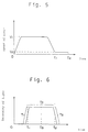
- a film exposure method which is carried out by the above-described film exposure apparatus, comprising the steps of step-feeding one frame of a film by the film feed mechanism, driving the photomask position adjusting mechanism after step-feeding, thereby scanning a primary projection image of each of the photomask-side alignment marks in a region including corresponding one of the film-side alignment marks on the stopped one frame, while permitting light transmitted through the film-side alignment marks to be applied to the detector, storing positions at equal output levels in rising and falling curves of an output signal from the detector, driving the photomask position adjusting mechanism, so that an image of each of the photomask-side alignment marks may be aligned with corresponding one of the film-side alignment marks on the basis of the stored positions, and effecting an exposure.
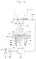
- a film feed mechanism 60 feeds one frame F10 of the film F to a position to which the image is projected by the projecting lens 20.
- a feed roller 61 is driven by a motor 62, and then stopped by a signal from the system controller 50 which has received a signal from the detecting system 40.
- Reference numeral 63 is a retaining roller; 64 being a sprocket roller; 65 is a retaining roller; 66 and 67 being each an auxiliary roller; 68 being an unwind reel; and 69 being a wind-up reel.
- the alignment of the photomask M after step-feeding is carried out in the following manner:
Landscapes
- Physics & Mathematics (AREA)
- General Physics & Mathematics (AREA)
- Exposure And Positioning Against Photoresist Photosensitive Materials (AREA)
Description
Claims (6)
- A film exposure apparatus for sequentially exposing to light a plurality of frames arranged in a longitudinal direction of a belt-shaped film being provided with at least two or more film-side alignment marks on each frame for formation of an image onto each of the frames, comprising:an illumination system (10);a photomask holding mechanism (Mll) for receiving, at a location to which light from the illumination system is applied, a photomask being provided with a circuit pattern whose image is to be projected and transferred onto the film, and with photomask-side alignment marks (MM) in correspondence to the film-side alignment marks,a projection lens (20) for projecting, upon irradiation from said illumination system, an image of a photomask received in said photomask holding mechanism;a film feed mechanism (60) for step-feeding the film one frame by one frame; anda photomask position adjusting mechanism (M10) for adjusting the position of the photomask holding mechanism corresponding to each frame to be exposed of a belt-shaped film positioned at the exposure stage on the basis of the alignment marks on said photomask and said film.
- A film exposure apparatus according to claim 1, being adapted to adjust said position on the basis of film-side alignment marks which are formed by a hole or a transparent portion in the film.
- A film exposure apparatus according to claim 2, further including an optical system (41, 42) for projecting a primary projection image (MM') of the photomask-side alignment mark (MM) projected to a position of projection of the image by the projection lens (20),
and a detector (43) adapted to receive a secondary projection image provided by said optical system. - A film exposure apparatus according to claim 3, further including a second optical system (46) for projecting a primary projection image (MM') of the photomask-side alignment mark (MM) in a divided manner even to a position different from a position at which the detector (43) is mounted, an image sensor (71) adapted for receiving a secondary projection image provided by the second optical system (46), and a monitor (72) mechanism associated with the image sensor (71).
- A film exposure process for sequentially exposing to light a plurality of frames arranged in a longitudinal direction of a belt-shaped film for formation of an image onto each frame, comprising the steps of:step-feeding each frame of a film by a film feed mechanism;adjusting the position of a photomask corresponding to said each frame to be exposed by driving a photomask position adjusting mechanism to align the photomask with said each frame so that images of photomask-side alignment marks are projected onto corresponding positions of film-side alignment marks on said each frame stopped after the step-feeding; andeffecting an exposure.
- A film exposure process according to claim 5, wherein said adjusting comprises the steps of:scanning a primary projection image of each of the photomask-side alignment marks in a region including corresponding one of the film-side alignment marks on the stopped one frame, while permitting light transmitted through the film-side alignment marks to be applied to the detector;storing positions at equal output levels in rising and falling curves of an output signal from the detector;driving the photomask position adjusting mechanism so that an image of each of the photomask-side alignment marks may be aligned with corresponding one of the film-side alignment marks on the basis of the stored positions.
Applications Claiming Priority (2)
| Application Number | Priority Date | Filing Date | Title |
|---|---|---|---|
| JP81336/90 | 1990-03-30 | ||
| JP8133690 | 1990-03-30 |
Publications (3)
| Publication Number | Publication Date |
|---|---|
| EP0449180A2 EP0449180A2 (en) | 1991-10-02 |
| EP0449180A3 EP0449180A3 (en) | 1992-05-13 |
| EP0449180B1 true EP0449180B1 (en) | 1998-06-03 |
Family
ID=13743533
Family Applications (1)
| Application Number | Title | Priority Date | Filing Date |
|---|---|---|---|
| EP91104681A Expired - Lifetime EP0449180B1 (en) | 1990-03-30 | 1991-03-25 | Film exposure apparatus and method of exposure using the same |
Country Status (3)
| Country | Link |
|---|---|
| US (1) | US5198857A (en) |
| EP (1) | EP0449180B1 (en) |
| DE (1) | DE69129509T2 (en) |
Cited By (1)
| Publication number | Priority date | Publication date | Assignee | Title |
|---|---|---|---|---|
| DE10064292C1 (en) * | 2000-12-22 | 2002-10-31 | Karl Suess Kg Praez Sgeraete F | Device for transporting a film |
Families Citing this family (16)
| Publication number | Priority date | Publication date | Assignee | Title |
|---|---|---|---|---|
| US5363171A (en) * | 1993-07-29 | 1994-11-08 | The United States Of America As Represented By The Director, National Security Agency | Photolithography exposure tool and method for in situ photoresist measurments and exposure control |
| US5652645A (en) * | 1995-07-24 | 1997-07-29 | Anvik Corporation | High-throughput, high-resolution, projection patterning system for large, flexible, roll-fed, electronic-module substrates |
| JP3376935B2 (en) * | 1999-01-25 | 2003-02-17 | ウシオ電機株式会社 | Exposure equipment for strip-shaped workpieces |
| US6278483B1 (en) | 1999-03-25 | 2001-08-21 | Eastman Kodak Company | Image registration on repeated scans using fiducial marks |
| JP2006102991A (en) * | 2004-09-30 | 2006-04-20 | Fuji Photo Film Co Ltd | Image recording device and image recording method |
| KR101136444B1 (en) * | 2006-06-07 | 2012-04-19 | 브이 테크놀로지 씨오. 엘티디 | Exposure method and exposure apparatus |
| JP4386929B2 (en) * | 2007-04-09 | 2009-12-16 | 日東電工株式会社 | TAB tape carrier manufacturing method |
| WO2009011119A1 (en) * | 2007-07-13 | 2009-01-22 | Nikon Corporation | Pattern formation method and device, exposure method and device, and device manufacturing method and device |
| JP5144992B2 (en) * | 2007-08-27 | 2013-02-13 | 株式会社オーク製作所 | Exposure equipment |
| EP2095946A1 (en) * | 2008-02-27 | 2009-09-02 | Nederlandse Organisatie voor toegepast- natuurwetenschappelijk onderzoek TNO | A system for patterning flexible foils |
| WO2010075158A1 (en) | 2008-12-23 | 2010-07-01 | 3M Innovative Properties Company | Roll-to-roll digital photolithography |
| US8610986B2 (en) * | 2009-04-06 | 2013-12-17 | The Board Of Trustees Of The University Of Illinois | Mirror arrays for maskless photolithography and image display |
| KR101948467B1 (en) * | 2010-02-12 | 2019-02-14 | 가부시키가이샤 니콘 | Substrate processing device and substrate processing method |
| JP5538049B2 (en) | 2010-04-22 | 2014-07-02 | 日東電工株式会社 | Method for aligning photomask and substrate and method for manufacturing printed circuit board |
| JP5538048B2 (en) | 2010-04-22 | 2014-07-02 | 日東電工株式会社 | Alignment mark detection method and printed circuit board manufacturing method |
| JP6510768B2 (en) * | 2014-05-23 | 2019-05-08 | 株式会社オーク製作所 | Exposure device |
Family Cites Families (8)
| Publication number | Priority date | Publication date | Assignee | Title |
|---|---|---|---|---|
| US3689991A (en) * | 1968-03-01 | 1972-09-12 | Gen Electric | A method of manufacturing a semiconductor device utilizing a flexible carrier |
| US4109158A (en) * | 1976-05-27 | 1978-08-22 | Western Electric Company, Inc. | Apparatus for positioning a pair of elements into aligned intimate contact |
| JPS55149929A (en) * | 1979-05-10 | 1980-11-21 | Dainippon Screen Mfg Co Ltd | Positioning method of projected image in projection enlarger |
| US4980718A (en) * | 1986-06-24 | 1990-12-25 | Salter Stephen H | Registration method in photolithography and equipment for carrying out this method |
| SE453882B (en) * | 1986-07-24 | 1988-03-14 | Johansson Eva | TOPIC FOR CLOTHING AND USING THE TOPIC TO MAKE A CLOTHING |
| US4855792A (en) * | 1988-05-13 | 1989-08-08 | Mrs Technology, Inc. | Optical alignment system for use in photolithography and having reduced reflectance errors |
| JP2682840B2 (en) * | 1988-05-27 | 1997-11-26 | マミヤ・オーピー株式会社 | Film positioning method in exposure apparatus and apparatus therefor |
| JP2790469B2 (en) * | 1988-11-24 | 1998-08-27 | ウシオ電機株式会社 | Film exposure equipment |
-
1991
- 1991-03-19 US US07/671,534 patent/US5198857A/en not_active Expired - Lifetime
- 1991-03-25 DE DE69129509T patent/DE69129509T2/en not_active Expired - Fee Related
- 1991-03-25 EP EP91104681A patent/EP0449180B1/en not_active Expired - Lifetime
Cited By (1)
| Publication number | Priority date | Publication date | Assignee | Title |
|---|---|---|---|---|
| DE10064292C1 (en) * | 2000-12-22 | 2002-10-31 | Karl Suess Kg Praez Sgeraete F | Device for transporting a film |
Also Published As
| Publication number | Publication date |
|---|---|
| US5198857A (en) | 1993-03-30 |
| EP0449180A2 (en) | 1991-10-02 |
| EP0449180A3 (en) | 1992-05-13 |
| DE69129509D1 (en) | 1998-07-09 |
| DE69129509T2 (en) | 1998-10-01 |
Similar Documents
| Publication | Publication Date | Title |
|---|---|---|
| US5198857A (en) | Film exposure apparatus and method of exposure using the same | |
| US6137562A (en) | Substrate adjuster, substrate holder and substrate holding method | |
| US5881165A (en) | Process for the positioning of a mask relative to a workpiece and device for executing the process | |
| US5317615A (en) | Exposure apparatus | |
| US6459491B1 (en) | Non-intrusive pellicle height measurement system | |
| US4127777A (en) | Method for automatic adjustment | |
| US4798470A (en) | Pattern printing method and apparatus | |
| EP1293836B1 (en) | Device for exposure of a strip-shaped workpiece with a meander correction device | |
| EP0443106B1 (en) | Exposure apparatus | |
| KR100246574B1 (en) | Reticle Aligner and Method | |
| US5161176A (en) | Exposure apparatus | |
| JP2886675B2 (en) | Film exposure apparatus and film exposure method | |
| US5825468A (en) | Exposure system for lithography apparatus | |
| JP2815724B2 (en) | Method of aligning film and reticle in film exposure apparatus | |
| IE51237B1 (en) | Improved step-and-repeat projection alignment and exposure system with auxiliary optical unit | |
| US4648708A (en) | Pattern transfer apparatus | |
| JP2880317B2 (en) | Film exposure method | |
| JP2892149B2 (en) | Positioning apparatus and film exposure apparatus using the apparatus | |
| JP2696973B2 (en) | Pattern exposure apparatus and peripheral exposure method | |
| JP2759898B2 (en) | Focus detection method in film exposure apparatus | |
| USH1463H (en) | Method for detecting positions of photomask and substrate | |
| JP3152133B2 (en) | Mask and work alignment method and apparatus | |
| KR0151252B1 (en) | Flat edge exposure device for water | |
| JP2786946B2 (en) | Film exposure apparatus and film exposure method | |
| JP3413947B2 (en) | Peripheral exposure equipment |
Legal Events
| Date | Code | Title | Description |
|---|---|---|---|
| PUAI | Public reference made under article 153(3) epc to a published international application that has entered the european phase |
Free format text: ORIGINAL CODE: 0009012 |
|
| 17P | Request for examination filed |
Effective date: 19910325 |
|
| AK | Designated contracting states |
Kind code of ref document: A2 Designated state(s): DE FR GB |
|
| PUAL | Search report despatched |
Free format text: ORIGINAL CODE: 0009013 |
|
| AK | Designated contracting states |
Kind code of ref document: A3 Designated state(s): DE FR GB |
|
| 17Q | First examination report despatched |
Effective date: 19951107 |
|
| GRAG | Despatch of communication of intention to grant |
Free format text: ORIGINAL CODE: EPIDOS AGRA |
|
| GRAG | Despatch of communication of intention to grant |
Free format text: ORIGINAL CODE: EPIDOS AGRA |
|
| GRAH | Despatch of communication of intention to grant a patent |
Free format text: ORIGINAL CODE: EPIDOS IGRA |
|
| GRAH | Despatch of communication of intention to grant a patent |
Free format text: ORIGINAL CODE: EPIDOS IGRA |
|
| GRAA | (expected) grant |
Free format text: ORIGINAL CODE: 0009210 |
|
| AK | Designated contracting states |
Kind code of ref document: B1 Designated state(s): DE FR GB |
|
| REF | Corresponds to: |
Ref document number: 69129509 Country of ref document: DE Date of ref document: 19980709 |
|
| ET | Fr: translation filed | ||
| PLBE | No opposition filed within time limit |
Free format text: ORIGINAL CODE: 0009261 |
|
| STAA | Information on the status of an ep patent application or granted ep patent |
Free format text: STATUS: NO OPPOSITION FILED WITHIN TIME LIMIT |
|
| 26N | No opposition filed | ||
| REG | Reference to a national code |
Ref country code: GB Ref legal event code: IF02 |
|
| PGFP | Annual fee paid to national office [announced via postgrant information from national office to epo] |
Ref country code: GB Payment date: 20090324 Year of fee payment: 19 |
|
| PGFP | Annual fee paid to national office [announced via postgrant information from national office to epo] |
Ref country code: DE Payment date: 20090429 Year of fee payment: 19 |
|
| PGFP | Annual fee paid to national office [announced via postgrant information from national office to epo] |
Ref country code: FR Payment date: 20090325 Year of fee payment: 19 |
|
| GBPC | Gb: european patent ceased through non-payment of renewal fee |
Effective date: 20100325 |
|
| REG | Reference to a national code |
Ref country code: FR Ref legal event code: ST Effective date: 20101130 |
|
| PG25 | Lapsed in a contracting state [announced via postgrant information from national office to epo] |
Ref country code: FR Free format text: LAPSE BECAUSE OF NON-PAYMENT OF DUE FEES Effective date: 20100331 |
|
| PG25 | Lapsed in a contracting state [announced via postgrant information from national office to epo] |
Ref country code: DE Free format text: LAPSE BECAUSE OF NON-PAYMENT OF DUE FEES Effective date: 20101001 |
|
| PG25 | Lapsed in a contracting state [announced via postgrant information from national office to epo] |
Ref country code: GB Free format text: LAPSE BECAUSE OF NON-PAYMENT OF DUE FEES Effective date: 20100325 |