EP0447980A2 - Logarithmischer Verstärker mit Verstärkungsregelung - Google Patents
Logarithmischer Verstärker mit Verstärkungsregelung Download PDFInfo
- Publication number
- EP0447980A2 EP0447980A2 EP91104030A EP91104030A EP0447980A2 EP 0447980 A2 EP0447980 A2 EP 0447980A2 EP 91104030 A EP91104030 A EP 91104030A EP 91104030 A EP91104030 A EP 91104030A EP 0447980 A2 EP0447980 A2 EP 0447980A2
- Authority
- EP
- European Patent Office
- Prior art keywords
- coupled
- terminal
- transistor
- emitter
- input
- Prior art date
- Legal status (The legal status is an assumption and is not a legal conclusion. Google has not performed a legal analysis and makes no representation as to the accuracy of the status listed.)
- Granted
Links
Images
Classifications
-
- G—PHYSICS
- G06—COMPUTING OR CALCULATING; COUNTING
- G06G—ANALOGUE COMPUTERS
- G06G7/00—Devices in which the computing operation is performed by varying electric or magnetic quantities
- G06G7/12—Arrangements for performing computing operations, e.g. operational amplifiers
- G06G7/24—Arrangements for performing computing operations, e.g. operational amplifiers for evaluating logarithmic or exponential functions, e.g. hyperbolic functions
Definitions
- This invention relates to logarithmic amplifiers, and more particularly, to logarithmic amplifiers wherein the gain is easily changed to accomodate a range of input signal currents.
- Logarithmic amplifiers are used in applications where there is a need to compress an input having a large dynamic range into an output having a small dynamic range.
- the linear gain factor imposed on the logarithmic output voltage was either a fixed function or not easily changed. What is desired is a logarithmic amplifier having an easily changible gain in order that a range of input signal currents may be accomodated and in order that the dynamic range requirements of linear amplifiers following the logarithmic amplifier may be relaxed.
- a logarithmic amplifier includes a first diode wherein the anode receives an input signal current and a standing current.
- the cathode of the first diode is coupled to the emitter of a PNP transistor.
- the collector of the PNP transistor is coupled to the anode of a second diode.
- a bias current is added to the emitter and subtracted from the collector of the PNP transistor to provide a lower emitter impedance.
- the cathode of the second diode is coupled to a negative supply voltage through a load resistor.
- a feedback network including an emitter coupled pair of NPN transistors samples the voltage at the anode of the second diode and sinks a current from the base of the PNP transistor.
- the voltage at the anode of the first diode is amplified to provide a logarithmic output voltage.
- the output voltage may be attenuated and applied to the base of the PNP transistor.
- a feature of the present invention is to provide a logarithmic amplifier wherein the gain is easily adjustable.
- Another feature of the present invention is to provide a logarithmic amplifier wherein the gain may be optimized to provide a maximum dynamic range of output voltage for a given input current.
- Yet another feature of the present invention is to provide a logarithmic amplifier that is capable of operating at high frequencies greater than 100Mhz.
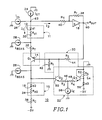
- a logarithmic amplifier 10 is shown in the schematic diagram of FIG. 1.
- the anode of a first diode 11 receives a portion of an input signal current 26, i IN , and a standing or biasing current 24, I ST , at node 62.
- the portion of the input signal current that flows into the first diode 11 is designated I 1.
- Diode 11 is shown as consisting of an ideal diode 12 designated d1 and a parasitic resistance 30 designated R d 1 .
- a PNP transistor 14 has an emitter coupled to the cathode of the first diode 11.
- PNP transistor 14 is shown as consisting of an ideal transistor Q 1 and a parasitic resistance 32 designated R T .
- a bias current 28 designated I BIAS is added to the standing current 24 at the emitter of PNP transistor 14. The same bias current 28 is subtracted from the collector of PNP transistor 14. The bias current 28 flows only through PNP transistor 14 and is used to decrease the emitter impedance of the transistor.
- the anode of a second diode 15, shown as ideal diode 16 designated d2 and a parasistic resistance 34 designated R d 2 is coupled to the collector of PNP transistor 14.
- a load element, resistor 36 designated R c couples the cathode of the second diode 15 to a -5 volt power supply.
- a feedback network 22 samples the voltage at the anode of the second diode 15 and compares this voltage to a reference voltage.
- the output of the feedback network 22 is an error current that is coupled to the base of PNP transistor 14.
- the means for generating the error current includes NPN transistors 50 and 52 designated Q 2 and Q3 .
- the emitters of NPN transistors 50 and 52 are coupled together and to an emitter current source 58 designated I E through emitter resistors 46 and 48, designated R 3 and R 4 to form a differential amplifier.
- an output error current is formed at the collector of NPN transistor 50 if the voltage at the base of NPN transistor 50 is unequal to the voltage at the base of NPN transistor 52.
- the voltage at the base of NPN transistor 52 is provided by a reference voltage generator including a bias element, resistor 54 designated R 5, and a third diode 56 designated d3.
- the voltage provided by the reference voltage generator tracks the thermal variations in the voltage at the anode of the second diode 15. Therefore the error current at the collector of NPN transistor 50 is only a function of the voltage at the anode of the second diode 15 attributable to the input signal current, i IN .
- a second current path is established through an input resistor 40 designated R I and a feedback resister 38 designated R f .
- the current flowing through the input resistor 40 and feedback resistor 38 is designated I 2.
- Operational amplifier 18 that is configured to provide a negative gain equal to R f /R I amplifies the voltage at node 62 to provide the output voltage at node 60 designated e OUT .
- the logarithmic output voltage e OUT is attenuated by an attenuation network 20 and applied to the base of PNP transistor 14.
- the attenuation network 20 includes a series resistance 44 designated R 2 and a shunt resistance 42 designated R 1.
- e 1 is the voltage at node 62
- e 2 is the voltage at the cathode of ideal diode d1
- e 3 is the voltage at the anode of the second diode 15
- e 4 is the voltage at the base of PNP transistor 14.
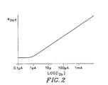
- Equation [16] is the final equation that demonstrates the logarithmic output voltage with respect to a linear input current. It is important to note that the undesirable effect of the parasitic resistance in the diodes and PNP transistor on the logarithmic gain characteristic has been removed. However, this equation is transcendental and the output voltage, e out , cannot be written as a direct function of the input current, I IN . Therefore the graphical representation of equation [16] is shown in FIG. 2.
- Figure 2 is a graph that shows the output voltage as a function of the logarithm of the input signal current. For currents higher than approximately 1 ⁇ A, the logarithmic amplifier according to the present invention provides a logarithmic output that is represented by a straight line on the graph.
- the output voltage is a linear function of the input current and is represented by the curved line on the graph. This linear portion of the gain characteristics of the logarithmic amplifier is useful for averaging low level input signal currents to ascertain the signal level as the noise level becomes significant.
- Schottky diodes be used for diodes 11 and 15.
Landscapes
- Physics & Mathematics (AREA)
- Engineering & Computer Science (AREA)
- Mathematical Physics (AREA)
- Theoretical Computer Science (AREA)
- Software Systems (AREA)
- Computer Hardware Design (AREA)
- General Physics & Mathematics (AREA)
- Tone Control, Compression And Expansion, Limiting Amplitude (AREA)
- Amplifiers (AREA)
Applications Claiming Priority (2)
| Application Number | Priority Date | Filing Date | Title |
|---|---|---|---|
| US07/495,191 US5012140A (en) | 1990-03-19 | 1990-03-19 | Logarithmic amplifier with gain control |
| US495191 | 1990-03-19 |
Publications (3)
| Publication Number | Publication Date |
|---|---|
| EP0447980A2 true EP0447980A2 (de) | 1991-09-25 |
| EP0447980A3 EP0447980A3 (en) | 1992-01-22 |
| EP0447980B1 EP0447980B1 (de) | 1996-04-24 |
Family
ID=23967640
Family Applications (1)
| Application Number | Title | Priority Date | Filing Date |
|---|---|---|---|
| EP91104030A Expired - Lifetime EP0447980B1 (de) | 1990-03-19 | 1991-03-15 | Logarithmischer Verstärker mit Verstärkungsregelung |
Country Status (4)
| Country | Link |
|---|---|
| US (1) | US5012140A (de) |
| EP (1) | EP0447980B1 (de) |
| JP (1) | JPH0783228B2 (de) |
| DE (1) | DE69118957T2 (de) |
Families Citing this family (10)
| Publication number | Priority date | Publication date | Assignee | Title |
|---|---|---|---|---|
| GB2241806B (en) * | 1990-03-09 | 1993-09-29 | Plessey Co Ltd | Improvements in true logarithmic amplifiers |
| US5221907A (en) * | 1991-06-03 | 1993-06-22 | International Business Machines Corporation | Pseudo logarithmic analog step adder |
| CH684805A5 (de) * | 1992-07-20 | 1994-12-30 | Balzers Hochvakuum | Verfahren zur Wandlung eines gemessenen Signals, Wandler zu dessen Ausführung sowie Messanordnung. |
| US5491548A (en) * | 1994-03-18 | 1996-02-13 | Tektronix, Inc. | Optical signal measurement instrument and wide dynamic range optical receiver for use therein |
| US5564092A (en) * | 1994-11-04 | 1996-10-08 | Motorola, Inc. | Differential feed-forward amplifier power control for a radio receiver system |
| GB9514490D0 (en) * | 1995-07-14 | 1995-09-13 | Nokia Telecommunications Oy | Improvements to a logarithmic converter |
| US5929982A (en) * | 1997-02-04 | 1999-07-27 | Tektronix, Inc. | Active APD gain control for an optical receiver |
| US6265928B1 (en) * | 1999-07-16 | 2001-07-24 | Nokia Telecommunications Oy | Precision-controlled logarithmic amplifier |
| JP3880345B2 (ja) * | 2001-08-27 | 2007-02-14 | キヤノン株式会社 | 差動増幅回路及びそれを用いた固体撮像装置並びに撮像システム |
| US9298952B2 (en) | 2013-11-18 | 2016-03-29 | King Fahd University Of Petroleum And Minerals | CMOS logarithmic current generator and method for generating a logarithmic current |
Family Cites Families (11)
| Publication number | Priority date | Publication date | Assignee | Title |
|---|---|---|---|---|
| US3678947A (en) * | 1970-07-16 | 1972-07-25 | Melvin J Davidson | Eyeliner |
| US3928774A (en) * | 1974-01-24 | 1975-12-23 | Petrolite Corp | Bipolar log converter |
| JPS52106054U (de) * | 1976-02-09 | 1977-08-12 | ||
| GB1571016A (en) * | 1976-02-20 | 1980-07-09 | Tokyo Shibaura Electric Co | Voltage controlled variable gain circuit |
| US4125789A (en) * | 1977-06-07 | 1978-11-14 | Sundstrand Corporation | Biasing and scaling circuit for transducers |
| DE2932655C2 (de) * | 1979-08-11 | 1982-03-04 | Hewlett-Packard GmbH, 7030 Böblingen | Impulsgenerator |
| US4418317A (en) * | 1981-05-18 | 1983-11-29 | Tektronix, Inc. | Logarithmic amplifier utilizing positive feedback |
| US4471324A (en) * | 1982-01-19 | 1984-09-11 | Dbx, Inc. | All NPN variably controlled amplifier |
| US4507615A (en) * | 1982-12-16 | 1985-03-26 | Tektronix, Inc. | Non-linear amplifier systems |
| SU1117660A1 (ru) * | 1983-03-28 | 1984-10-07 | Предприятие П/Я А-3726 | Логарифмический преобразователь |
| US4739283A (en) * | 1987-03-02 | 1988-04-19 | Tektronix, Inc. | Variable transient response control for linear integrated-circuit high-frequency amplifiers |
-
1990
- 1990-03-19 US US07/495,191 patent/US5012140A/en not_active Expired - Fee Related
-
1991
- 1991-03-15 DE DE69118957T patent/DE69118957T2/de not_active Expired - Fee Related
- 1991-03-15 EP EP91104030A patent/EP0447980B1/de not_active Expired - Lifetime
- 1991-03-19 JP JP3081031A patent/JPH0783228B2/ja not_active Expired - Lifetime
Also Published As
| Publication number | Publication date |
|---|---|
| JPH0783228B2 (ja) | 1995-09-06 |
| EP0447980A3 (en) | 1992-01-22 |
| JPH04219007A (ja) | 1992-08-10 |
| EP0447980B1 (de) | 1996-04-24 |
| DE69118957T2 (de) | 1996-10-24 |
| DE69118957D1 (de) | 1996-05-30 |
| US5012140A (en) | 1991-04-30 |
Similar Documents
| Publication | Publication Date | Title |
|---|---|---|
| US5128566A (en) | Variable attenuator circuit | |
| EP0447980A2 (de) | Logarithmischer Verstärker mit Verstärkungsregelung | |
| KR0148324B1 (ko) | 가변 이득 증폭 회로 | |
| JPS6133404B2 (de) | ||
| US3999139A (en) | Monolithic alternately stacked IF amplifier | |
| US4473780A (en) | Amplifier circuit and focus voltage supply circuit incorporating such an amplifier circuit | |
| JP3938793B2 (ja) | 擬似対数利得制御を用いる可変利得増幅器 | |
| EP0025977B1 (de) | Verstärker mit steuerbarer Verstärkung | |
| GB2081039A (en) | Gain control circuits | |
| US6466085B2 (en) | Amplifier circuit and preconditioning circuit for use in amplifier circuit | |
| US4625131A (en) | Attenuator circuit | |
| US7622981B2 (en) | Square cell having wide dynamic range and power detector implementing same | |
| US4418317A (en) | Logarithmic amplifier utilizing positive feedback | |
| JP3404209B2 (ja) | トランスインピーダンス増幅器回路 | |
| GB1579945A (en) | Audio-frequency power amplifiers | |
| US4077012A (en) | Amplifier devices | |
| JPS6012331Y2 (ja) | 2個のトランジスタを具える増幅回路 | |
| GB2081037A (en) | Gain control circuit | |
| GB2100541A (en) | Buffer amplifier | |
| US4385364A (en) | Electronic gain control circuit | |
| JP2619858B2 (ja) | 折線近似型関数発生回路 | |
| US3651420A (en) | Variable gain direct coupled amplifier | |
| US4963764A (en) | Low noise current mirror active load circuit | |
| EP0290277B1 (de) | Integrierte wirksame Lastschaltung mit niedrigem Geräusch | |
| JPH06120747A (ja) | 差動増幅器 |
Legal Events
| Date | Code | Title | Description |
|---|---|---|---|
| PUAI | Public reference made under article 153(3) epc to a published international application that has entered the european phase |
Free format text: ORIGINAL CODE: 0009012 |
|
| AK | Designated contracting states |
Kind code of ref document: A2 Designated state(s): DE FR GB |
|
| PUAL | Search report despatched |
Free format text: ORIGINAL CODE: 0009013 |
|
| AK | Designated contracting states |
Kind code of ref document: A3 Designated state(s): DE FR GB |
|
| 17P | Request for examination filed |
Effective date: 19920226 |
|
| 17Q | First examination report despatched |
Effective date: 19940818 |
|
| RAP1 | Party data changed (applicant data changed or rights of an application transferred) |
Owner name: TEKTRONIX, INC. |
|
| GRAH | Despatch of communication of intention to grant a patent |
Free format text: ORIGINAL CODE: EPIDOS IGRA |
|
| GRAA | (expected) grant |
Free format text: ORIGINAL CODE: 0009210 |
|
| AK | Designated contracting states |
Kind code of ref document: B1 Designated state(s): DE FR GB |
|
| PG25 | Lapsed in a contracting state [announced via postgrant information from national office to epo] |
Ref country code: FR Effective date: 19960424 |
|
| REF | Corresponds to: |
Ref document number: 69118957 Country of ref document: DE Date of ref document: 19960530 |
|
| EN | Fr: translation not filed | ||
| PLBE | No opposition filed within time limit |
Free format text: ORIGINAL CODE: 0009261 |
|
| STAA | Information on the status of an ep patent application or granted ep patent |
Free format text: STATUS: NO OPPOSITION FILED WITHIN TIME LIMIT |
|
| PG25 | Lapsed in a contracting state [announced via postgrant information from national office to epo] |
Ref country code: GB Effective date: 19970315 |
|
| 26N | No opposition filed | ||
| GBPC | Gb: european patent ceased through non-payment of renewal fee |
Effective date: 19970315 |
|
| PG25 | Lapsed in a contracting state [announced via postgrant information from national office to epo] |
Ref country code: DE Effective date: 19971202 |