EP0447751A2 - Système de normalisation de largeur - Google Patents
Système de normalisation de largeur Download PDFInfo
- Publication number
- EP0447751A2 EP0447751A2 EP91100646A EP91100646A EP0447751A2 EP 0447751 A2 EP0447751 A2 EP 0447751A2 EP 91100646 A EP91100646 A EP 91100646A EP 91100646 A EP91100646 A EP 91100646A EP 0447751 A2 EP0447751 A2 EP 0447751A2
- Authority
- EP
- European Patent Office
- Prior art keywords
- data
- cell
- dot
- histogram
- supplied
- Prior art date
- Legal status (The legal status is an assumption and is not a legal conclusion. Google has not performed a legal analysis and makes no representation as to the accuracy of the status listed.)
- Granted
Links
Images


Classifications
-
- G—PHYSICS
- G06—COMPUTING OR CALCULATING; COUNTING
- G06V—IMAGE OR VIDEO RECOGNITION OR UNDERSTANDING
- G06V30/00—Character recognition; Recognising digital ink; Document-oriented image-based pattern recognition
- G06V30/10—Character recognition
- G06V30/16—Image preprocessing
- G06V30/166—Normalisation of pattern dimensions
-
- G—PHYSICS
- G06—COMPUTING OR CALCULATING; COUNTING
- G06V—IMAGE OR VIDEO RECOGNITION OR UNDERSTANDING
- G06V30/00—Character recognition; Recognising digital ink; Document-oriented image-based pattern recognition
- G06V30/10—Character recognition
Definitions
- This invention pertains to a data processing system for an image processing device,and more particularly, to a data processing system for converting image data to a target area size, for obtaining histograms as judging factors for calculating the character coordinates using a two-port RAM, for expediting the pre-treatment of image data in a character recognition operation by a character recognition device, for creating a conversion table for normalizing an extracted character pattern in a systolic array structure for a character recognition device, and for normalizing the input pattern size in a systolic array structure in a pattern recognition device.
- One of many normalizing methods is to obtain histograms of an extracted character vertically and horizontally. Characters are magnified or contracted to be normalized from the obtained histograms.
- this normalizing method has the disadvantage that it consumes much time to obtain the histograms, because the CPU performs processing for magnification or contraction in one-dot units.
- Feature data of stored characters are read from a dictionary in character units and are then compared with the feature data of an inputted character to obtain a recognition. This has the disadvantage that the comparison takes much time.
- This invention aims at realizing a data processing system which enables a simple circuit to magnify or contract dot rows in parallel, expedites histogram calculation by using a two-port DRAM, enables a character recognition device to speed up pre-treatment of high-speed character recognition for a large volume of data, rushes pattern recognition by parallelly processing histogram information for normalizing extracted character data in a pipeline, and has a systolic array speed up pattern recognition by parallelly processing inputted data in a pipeline.
- reading devices for receiving image data, extracting characters from received image data and recognizing respective characters in sentences of the read documents are realized.
- These reading devices divide dot data read, e.g. by an image scanner, into predetermined areas and compare the character within a divided area with characters registered in the dictionary, and outputs the most similar character as the result.
- Registered character data are generally stored in a dictionary memory which memorizes e.g. featuring data of the respectively defined characters.
- a character to be recognized is inputted, the inputted character is similarly featured, so that the distance from the characters, i.e. the difference between it and the characters, stored in the dictionary memory is obtained.
- the stored character with the least distance is then outputted as the recognition result.
- all the processings are performed in one-dot units. For instance, processings for dividing data read e.g. by an image scanner in predetermined area units are performed in one-dot units.
- histograms in the vertical and horizontal directions are obtained.
- the differences between the maximums and the minimums of the histograms determines the frame area for each character unit.
- extracted characters are conventionally normalized to a predetermined height and width vertically and horizontally in one-character units through magnification or contraction.
- a first principle of this invention is to have a simple transposing circuit normalize character data parallelly, instead of in one-dot units, in two normalizing processes with a card, thus simpifying the circuit and expediting the entire processings.
- a second principle of this invention is to have a recognition device expedite a histogram calculation, thus enabling a fast and accurate character extraction.
- a third principle of this invention is to expedite various processings to be expedited by an exclusive programmable cell configured in a systolic array structure and processed parallelly in a pipeline.
- the programmable cell comprises a simple ALU, so it is inexpensive. Furthermore, it is programmable, so it can be commonly used for conversion table conversion, normalization, histogram calculation, and obliqueness adjustment.
- a fourth principle of this invention is to parallelly process histograms in a pipeline, so that normalization conversions are rushed, thus speeding up character recognition.
- a fifth principle of this invention is to utilize a systolic array to parallelly normalize characters in a pipeline for proper and faster character recognition, thus improving character recognition rate and speed.
- Figure 1A is a block diagram illustrating the first principle of this invention.
- a normalizing means 1-1 parallelly receives a part of plural dots in a particular line of image data and magnifies or contracts the received data in a direction horizontal to said line.
- the normalizing means 1-1 comprises the parallelly inputted dot number of latch circuits and "OR” gates, and stores the result of "OR” adding inputted dots and data outputted from said latch circuits in said latch circuits.
- the transposing means 1-2 transposes image data magnified or contracted along one side and obtained from said normalizing means 1-1 and re-inputs the transposed image data in said normalizing means 1-1.
- the normalizing means 1-1 magnifies or contracts an inputted character in a first input
- the transposing means 1-2 supplies magnified or contracted dots in dot column units to the normalizing means 1-1 and re-magnifies or re-contracts the supplied dots
- image data are magnified or contracted in both vertical and horizontal directions in two magnifying or contracting actions.
- Figure 1B is a block diagram illustrating the second principle of this invention.
- a two-port DRAM 2-1 memorizes image data supplied in dot units and sequentially outputs dots in a direction vertical to the inputted dot data. This is done, for instance, by providing a parallel-in/serial-out shift register in the two-port DRAM 2-1, memorizing dot data along one side by a first address and simultaneously reading out dot data along the other side by a second address for storing dot data in the shift register. Upon a receipt of a shift clock pulse, dots in a direction vertical to the inputted dot data are sequentially obtained.
- a counter 2-2 counts the number of 1 or 0 among the dot outputs.
- a selecting means 2-3 is a selecting circuit for selectively outputting input to or output from the two-port DRAM 2-1. This circuit is obtained, e.g. by selectively activating one of tri-state buffers provided at input and output terminals of the two-port DRAM 2-1.
- the two-port DRAM 2-1 dot-serially receives image data dots in scanning units, changes one address to an address in one scanning to be memorized in dot units. When one screen terminates, the other address specifies the direction vertical to the inputted scanning direction. Thus, dot data in the vertical direction in the two-port DRAM 2-1 are supplied to the shift register. By supplying a shift clock pulse to the shift register, dot data in the direction vertical to the scanning are serially outputted.
- the selecting means 2-3 selects the input and the counter 2-2 selects 1 or 0 for the dot.
- the selecting means 2-3 selects a shift output from the two-port DRAM 2-1
- the counter 2-2 counts the number of 1 or 0 of the dots in the direction vertical to the scanning direction.
- This counter 2-2 receives dot data at its enable terminal and clock pulses at its clock terminal and counts the number of 0 or 1.
- the above circuit operations count the number of dots, e.g. in the horizontal direction at an input time and in the vertical direction at an output time, histograms in the horizontal and vertical directions are obtained at high speeds.
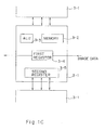
- Figure 1C is a block diagram illustrating the third principle of this invention.
- a cell 3-1 comprises a memory 3-2, an ALU 3-3, a first register 3-4, and a second register 3-4 connected in a systolic array form.
- the memory 3-2 memorizes inputted dot data and a program for processing data supplied from the cell neighboring in the direction vertical to the direction along which the dot data are inputted.
- the ALU 3-3 at least adds and compares data processed by the above program.
- the first register 3-4 memorizes the inputted data and outputs them to the next stage.
- the second register 3-5 memorizes the above processing result and outputs it to the neighboring cell opposite to the above neighboring cell.
- Each cell 3-1 configured in a systolic array structure processes image data received in dot units.
- the memory 3-2 memorizes the program for processing image data and the cell 3-1 executes the program so that simple operations such as additions and comparisons are performed, and supplies the result to the second register 3-5.
- the cell outputted from the second register 3-5 and the opposite neighboring cell supply the results, and operations are processed using the results and the image data memorized in the first register 3-4.
- the results are supplied to the second register 3-5 as well as outputted to neighboring cells.
- the dot data memorized by the first register 3-4 are also supplied to the cell in the next stage which performs similar processing in a sequential manner.
- the cell 3-1 Since the cell 3-1 is in a systolic array structure, the cell 3-1 outputs the inputted plural dot data to the next stage after an operation dot by dot as well as to neighboring cells, dot data related in the direction vertical to the input direction can be processed (in parallel) and further in a pipeline, various processings can be operated at high speeds. Since the operations necessary for the processing are additions or comparisons, the cell 3-1 can be configured by a simple ALU 3-3 and the price of the cell 3-1 can be lowered.
- Figure 1D is a block diagram illustrating the fourth principle of this invention.
- N pieces of serial circuits each serially connecting N pieces of cells H(1,1) through H(N,1),
- the m-th cell from the input side is a histogram calculating cell and the remaining cells are all shift registers.
- the histogram calculating cells shift the input data for outputting them to the next cells, update the count data and width data supplied from the cells one stage before in the neighboring columns, and output the results to the cells one stage after in the neighboring columns on the opposite side.
- each histogram calculating cell comprises a flag register of the horizontal direction, a width register in the vertical direction and a counter.
- N bits of dots are supplied in dot position units corresponding to the N pieces of columns and are sequentially shifted.
- histogram calculating cells are provided in the direction diagonal to one dot row, when one dot row data are supplied from the lower portion of the systolic array, the first histogram calculating cell in the first column from the input side performs the histogram calculation in the vertical and horizontal directions. Each time data are shifted in the systolic array, histograms are calculated for the next row and the next column. (The next histogram calculating cell is provided in the upper right direction.) By sequentially repeating the procedures, the count values and the width results are sequentially outputted from the last histogram calculating cell uppermost and most right. The register or the counter in the respective histogram calculating cell retain the count value or the width data in the opposite direction.
- Figure 1E is a block diagram illustrating the fifth principle of this invention.
- a normalizing cell P(q,n) receives information from the corresponding cell and the neighboring cells. That is, three pieces of information are supplied from the cell in the earlier stage and the right and left cells neighboring the cell. N pieces of such cells are parallelly configured to form a systolic array of Q stages.
- Normalizing cells P(q,1) through P(q,n) supply the dot data in the row direction along which the image is to be normalized, and these cells receive the data of the cells respectively neighboring the cells opposite to the above neighboring cells, when the product of the normalized value and the conversion value is greater than the product of the maximum width and the corresponding cell position.
- Data obtained at respective normalizing cells P(q,1) through P(q,n) are supplied to the normalizing cells P(q-1,1) through P(q-1,n) in the next stage to be processed similarly. Those procedures are performed sequentially. For instance, in case of a normalizing cell P(3,3), its neighboring cell is P ( 3,2) and its opposite normalizing cell is P(3,4).
- the target area character is magnified or contracted to a normalized area.
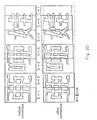
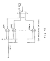
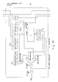
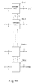
- Figure 2A shows a system configuration of a character-recognizing device using an image data normalization circuit of this invention.
- Image Information read by e.g. an image scanner is stored in an image memory 10 as image data.
- the image memory 10 has memory capacity for a page read by the image scanner.
- Each dot of the read information is stored as two-value data of either white or black, i.e. 0 or 1.
- Image data stored in the image memory 10 are supplied to a noise reduction module 11, where noise generated during reading time is eliminated.
- the eliminated noise is irrelevant to the character information.
- the noise reduction module 11 treats as white a black dot in a center of a three-by-three mask pattern in which only the dot in the center is black and the eight surrounding dots are white.
- the configuration of this invention provides the noise reduction module 11 to operate in a character recognition pre-treatment part 12, it could be set to operate at some other time, e.g., when the read image data are stored in character units in a normalization module 16 to be described later. Alternatively, it could be at a time of line-narrowing or stroking.
- the image data which have undergone a noise elimination through the noise reduction module 11 are supplied to a row-histogram module 13, a column-histogram module 14 and a read control module 15.
- the row-histogram module 13 projects the read information, e.g. the content of the form read by the image scanner described earlier, in the row direction and finds the number of dots in each dot row. That is, it finds the number of black dots in each dot row (in the horizontal direction).
- the column-histogram module 14 projects the read information in the column direction and finds the number of dots in each dot unit column.
- the row-histogram module 13 sequentially counts the number of black dots (for each dot row) in data sequentially read in one dot unit in the row direction from the image memory 10 (similarly to a dot reading by a raster scan) and supplied through the noise reduction module 11. That is, the row-histogram module 13 sequentially finds the number of black dots in each row.
- the numbers of black dots in respective rows form a row histogram.
- the column-histogram module 14 has counters each corresponding to a black dot position in a dot row, and increments the counter corresponding to the black dot position when a dot in a row is sequentially supplied.
- the row-histogram module 13 and the column-histogram module 14 respectively obtain a row histogram and a column histogram each representing the numbers of dots in row positions and column positions. The result is supplied to the read control module 15.
- the read control module 15 sequentially obtains the row position and the column position from the row histogram and the column histogram, respectively. These positions can be found, for instance, by a cycle of the row histogram or the column histogram.
- the read control module 15 finds the row and column positions and performs the following additional processings.
- Image data e.g. information read by an image scanner
- the read control module 15 sequentially changes the angle wherewith a histogram is obtained, so that an adjusted angle is obtained.
- the image data supplied from the noise reduction module 11 are reinputted to obtain the final histogram, so that row data for one cycle period corresponding to the obliqueness are read from the point whence the row histogram (having a maximum value) obtained from the adjusted obliqueness changes from zero to a positive number (or from a positive number to zero) and stored in a row buffer provided in the read control module 15.
- the read control module 15 again obtains a column histogram in a row from the row data stored in the row buffer and cuts out data of one character area to be outputted to a normalization module 16 and a conversion table creation module 17 from the point whence the column histogram changes from zero to a positive number.
- the conversion table creation module 17 is for obtaining conversion data for enabling the normalization module 16 to normalize a character.
- the conversion table creation module 17 projects the data of one character area extracted by the read control module 15 in the column and row directions, thereby incrementing the respective counters in the column and row directions by the dot row unit and by the dot column unit from the column and row with a black dot, to obtain the final counter value in one character area.
- the normalization module 16 magnifies the size of one character area from the size when the character in the character area is originally extracted, per the final counter values in the row and column directions of the dots in the extracted character, to the full sized character e.g. comprising sixty-four (64) by sixty-four (64) dots.
- the normalization module 16 converts a forty-eight (48) by forty-eight (48) dot character to a sixty-four (64) by sixty-four (64) dot character, where row and column dot data of particular positions are repeatedly used as the same data in magnifying the character.
- a line-narrowing module 18 narrows the width of the character by using a mask of eleven (11) dots comprising a center dot and the eight (8) other dots in the surrounding three (3) by three (3) area as well as the second left dot and the second up dots from the center dot.
- a mask used in narrowing could be of nine (9) dots in the three (3) by three (3) dot area around the center dot.
- the width of a line around a dot of a character can be narrowed by a control of the earlier described mask whereby a center dot of a predetermined pattern is set to zero.
- lines of a character are set to a width of one dot.
- the narrowed line character, e.g. of sixty-four (64) by sixty-four (64) dots, obtained by the line-narrowing module 18 is supplied to a stroking module 19 for stroking.
- the stroking module 19 expresses a dot by a total of four kinds of strokes wherein there is a black dot above or below; right or left; right above or left below; and left above or right below an objective dot, i.e. a center dot. If the objective dot belongs to plural kinds of strokes among the four (4) kinds described above, a prioritization, e.g. the vertical direction first, the horizontal direction second, etc., for deciding the kind of stroke the objective dot belongs to. When the objective dot is white or the center dot value is zero (0), the stroke is not considered to exist.
- the stroking module 19 Since the stroking module 19 has five (5) cases wherein a stroke exists in any of four (4) directions, i.e. vertical, horizontal, slash, and back-slash directions, or does not exist, the state of each dot is expressed as a three (3) bit value.
- the resultant three (3) by sixty-four (64) by sixty-four (64) bits of information are supplied to a feature vector module 20.
- the feature vector module 20 divides the stroking information obtained at the earlier described stroking module 19 both horizontally and vertically in eight (8) dot units.
- a vector module area of a total of two hundred fifty-six (256) [sixteen (16) by sixteen (16)] dots comprises one of the divided areas, the area below it, the area to its right, and the area to its lower right, each having 64 dots.
- the feature vector module 20 counts whether or not any of the four kinds of strokes in the vertical, horizontal, slash and back-slash directions exists.
- a feature vector is obtained in a vector module area comprising sixteen (16) by sixteen (16) dots, since a vector module area is vertically or horizontally shifted by eight (8) dots, there are seven (7) feature vector areas in both the row and column directions. Therefore, each character has a total of forty-nine (49) [seven (7) by seven (7)] vector module areas for feature vectors.
- the feature vector module 20 When the feature vector module 20 counts the number of strokes in each of the four directions for the respective vector module areas described earlier, the feature vector module 20 weights each dot representing a directional stroke, such that a center part of a vector module area comprising sixteen (16) by sixteen (16) dots has a higher weight in obtaining a feature vector. The weight reduces with distance from the center.
- a dot representing a directional stroke in the center area comprising four (4) by four (4) dots has a weight of four (4);
- a dot representing a directional stroke in the surrounding harrow area comprising eight (8) by eight (8) dots, excluding the four (4) by four (4) dot area at the center has a weight of three (3);
- a dot representing a directional stroke in the outermost harrow area comprising sixteen (16) by sixteen (16) dots, excluding the twelve (12) by twelve (12) dot area at the center has a weight of one (1).
- an embodiment of this invention uses standard patterns of feature vectors for classification in each vector module area for a feature vector, such that a distance is found between a supplied unknown input and twenty (20) classes of standard patterns in each vector module area, in order to improve operation processing speed and recognition rate. That is, the distance is found between the feature vector of the character to be read in each vector module area obtained from the feature vector module 20 and the feature vector of a standard pattern in the vector module area.
- Each vector module area is classified into classes 1 through 20, and the order of the classes having class distances in respective vector modules is found from the smallest to the fifth-smallest.
- a distance computing module 21 calculates the distances by using a class dictionary 23-1 (memorizing standard patterns in class units) in a vector dictionary 26.
- a candidate dictionary 23-2 is used to calculate the distances for respective candidate characters. (At this time a switch SW selects the candidate dictionary 23-2.)
- An upper rank selection and score assignment module 22 determines the five (5) top-ranked classes described earlier and the scores of the corresponding classes in the respective vector module areas. That is, the upper rank selection and score assignment module 22 determines the scores given to the respective classes of the first to fifth ranks from the distances obtained by the distance computing module 21, i.e. the scores of the respective candidate characters. For instance, five (5) points are given to the candidate character having the smallest distance, and decremental points of four (4) through one (1 ) are given to respective classes having the second smallest to the fifth smallest distances. These procedures are performed for all forty-nine (49) vector module areas. The processing result of the upper rank selection and score assignment module 22 is supplied to a comprehensive rating module 24.
- the comprehensive rating module 24 is for calculating the degree of conformance between an input objective, i.e. an inputted character, and its candidate character, and operates in three modes comprising an association conformance mode rated by a score, and a one hundred percent conformance mode and an individual conformance mode each rated by a distance.
- the association conformance mode is for calculating the score of a candidate character from the vector module area corresponding to the candidate character stored in an association dictionary 23-3 and a class belonging to the vector module area.
- Figure 2B shows the configuration of an association dictionary.
- the association dictionary 23-3 stores the identifications for the classes to which the candidate characters belong in the respective vector module areas by using the identifications for the candidate characters in the respective vector module areas as the addresses.
- the association dictionary 23-3 stores only these data obtained by clustering sets of feature vectors corresponding to the identifications for the vector module areas of the respective candidate characters by their (weighted) distances.
- the class dictionary 23-1 of the same structure corresponding to the association dictionary 23-3 is created concurrently in the distance computing module 21.
- the one to be used is designated at a dictionary reference starting point. (By comprehensively rating each of the dictionaries divided by identifications for the candidate characters in parallel, they can be referenced at higher speeds.)
- the association dictionary 23-3 is a table describing the identifications "K" for the classes wherein a candidate character "a" belongs to a vector module area "m".
- the one hundred percent conformance mode and the individual conformance mode in the comprehensive rating module 24 are for calculating comprehensive rating value V(a) for each candidate character "a".
- the upper-rank candidate selection module 25 selects and outputs a plurality of characters, e.g. five ( 5 ) top-ranked characters that become the recognition results of the read image data.
- the upper-rank candidate selection module 25 is for selecting the five (5) top-ranked characters by ranking the candidate characters per the comprehensive rating value V(a).
- the descending/ascending order of the comprehensive rating value V(a) of the individual conformance mode is sequentially from the biggest for character association; and sequentially from the smallest for others.
- Its outputs are identifications for the candidate characters arrayed in a sorting result of the inputs (or the inputting order) and their comprehensive rating values V(a).
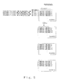
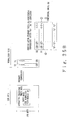
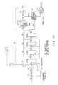
- Figure 3 shows in detail the circuit configuration of the row-histogram module 13 and the column-histogram module 14 using the first principle of this invention.
- the embodiment of this invention shown in Figure 3 provides a two-port DRAM 30 and a DRAM controller 31.
- the DRAM controller 31 specifies the addresses supplied to the two-port DRAM 30 at input and output times.
- the DRAM controller 31 supplies line data of a direction of the image data to the same column addresses as those specified earlier by sequentially changing row addresses of the two-port DRAM 30.
- the DRAM controller 31 is connected to an address bus and a data bus of a CPU 32.
- the CPU 32 controls the DRAM controller 31 for accessing the two-port DRAM 30, immediately before the read image data are supplied to the two-port DRAM 30 through the FIFO 35.
- the control by the CPU 32 makes the DRAM controller 31 sequentially access row addresses. After accessing the row addresses of one line, the DRAM controller 31 changes the column addresses.
- the outputs from the FIFO 35 i.e. data supplied to the input terminal of the two-port DRAM 30, are supplied to a tri-state buffer 33.
- the outputs from the two-port DRAM 30 are supplied to a tri-state buffer 34.
- the outputs from the tri-state buffer 33 and the tri-state buffer 34 are supplied commonly to a histogram counter 36.
- Either the tri-state buffer 33 or the tri-state buffer 34 is activated when the histogram counter 36 starts counting prompted by an instruction signal (not shown in the drawing) from the CPU 32.
- the histogram counter 36 is for counting a dot number in one direction along a line, e. g. one scanning direction or its vertical direction.
- a histogram memory 37 stores a result for each direction.
- the outputs from the histogram counter 36 are supplied not only to the histogram memory 37 but also to the data bus. If the DRAM controller 31 controls the histogram counter 36, e.g. when the histogram counter 36 outputs a counting result, the outputs from histogram counter 36 open the buses and have the histogram memory 37 memorize the addresses through the buses.
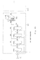
- Figure 4 explains in more detail the operations and the circuit configurations of a row-histogram module 13 and a column-histogram module 14 using the first principle of this invention described in Figure 3.
- the two-port DRAM 30 comprises a random memory 30-1 for storing the row addresses and the column addresses and a serial memory (line memory) 30-2.
- Vertical line data of the read image data (of n by m dots) are supplied dot-serially to the two-port DRAM 30.
- the two-port DRAM 30 stores the row addresses sequentially changed by the DRAM controller 31 while keeping the column addresses constant in a vertical line, so that the vertical line data are sequentially stored in the same column addresses.
- the DRAM controller 31 under the control of the CPU 32 has the random memory 30-1 store the transmitted image data (of n by m dots).
- the vertical line data are sequentially supplied to the histogram counter 36 in one-dot units by activating the tri-state buffer 33.
- the outputs from the tri-state buffer 33 are supplied to an enable terminal of the histogram counter 36 corresponding to a clock pulse supplied in one-dot units.
- the histogram counter 36 performs a counting.
- the histogram counter 36 does not perform it. That is, the histogram counter 36 counts the number of black dots whose value is "1". Since the results in vertical-line units are stored in the histogram memory 37 shown in Figure 3, a histogram in vertical-line units is stored in the histogram memory 37.
- a signal (not shown in the drawing) specifies row addresses. Dot data specified by the row addresses are transmitted to the serial memory 30-2. After the transmission controlled by the CPU 32, by applying a shift clock pulse SAS to the two-port DRAM 30, an output terminal SD of the two-port DRAM 30 outputs data (1 through n) corresponding to a row address in horizontal-line units.
- the tri-state buffer 34 is activated and supplies the dot data outputted from the output terminal SD of the two-port DRAM 30 are sequentially supplied to the histogram counter 36. Since outputs from the tri-state buffer 34 are supplied to the enable terminal of the histogram counter 36, dot data are counted in the horizontal direction, similarly to those in the vertical direction described earlier. The counted value is supplied to the histogram memory 37 in horizontal-line units, and the histogram memory 37 obtains the vertical and horizontal histogram results.
- Figure 5 shows in detail the circuit configurations of the row-histogram module 13 and the column-histogram module 14 using the first principle of this invention.
- Figure 6 shows schematically the configurations of the row-histogram module 13 and the column-histogram module 14 using the first principle of this invention.
- the second embodiment shown in Figure 5 uses a two-port DRAM 40 comprising n by m pieces of the two-port DRAMs 30 for processing in n bit units. That is, n pieces of dot data are supplied to the two-port DRAM 40 in a batch.
- a DRAM controller 41 is similar to the DRAM controller 31 shown in Figure 3 and is for controlling the two-port DRAM 40 each comprising n by m pieces of the two-port DRAMs 30 by supplying respective addresses and control signals.
- n pieces of these addresses for storing dot data are supplied in a batch to n pieces of the two-port DRAMs 30 in the two-port DRAM 40.
- n by m bits of dot data are stored in the two-port DRAM 40 comprising n by m pieces of the two-port DRAMs 30.
- image data of n dots are stored in a FIFO 45 before they are supplied to the two-port DRAM 40, and a CPU 42 controls the DRAM controller 41.
- n bits of dot data are stored in a batch in n pieces of the two-port DRAMs 30 grouped in the two-port DRAM 40.
- n by m bits of dot data are stored in the two-port DRAM 40.
- the outputs from the FIFO 45 are supplied to a tri-state buffer 43 as well as to the two-port DRAM 40.
- the n inputted bits of data are supplied to a histogram counter 46.
- the histogram counter 46 then counts the number of black dots included in these n bits of dot data received. That is, the histogram counter 46 comprises m pieces of counters, where m is no less than n.
- the outputs from the tri-state buffer 43 are supplied respectively to n pieces of counters among the above m pieces of counters.
- n by m pieces of the two-port DRAMs 30 in the two-port DRAM 40 parallelly output data in the direction vertical to their respective stored data. That is, n pieces of data comprising n by m bits (which is the number of the two-port DRAMs 30 in the two-port DRAM 40) are outputted.
- a parallel-to-serial conversion circuit 48 serially outputs the n bits by a further parallel-to-serial conversion of the n bits. Because a clock shifted by a frequency divider 49 is supplied to the respective input terminals for receiving the shift clock pulse SAS in the two-port DRAM 40, the two-port DRAM 40 simultaneously outputs n bits in synchronization with the shift clock pulse SAS. Accordingly, each time n bits are received, the parallel-to-serial conversion circuit 48 supplies the n bits to the histogram counter 46 through a tri-state buffer 44, by converting n bits from parallel data to serial data. Since the outputs from the parallel-to-serial conversion circuit 48 comprise n bits, the histogram counter 46 counts the respective n bits of dot data and supplies the result to the histogram memory 47.
- the two-port DRAM 40 as an image memory determines a bit width of one bank based on the transmitted image bit width, and the bank number is set equal to the the histogram counter number (i.e. limited by the histogram counter number), where m is never less than n.
- Figure 7 explains the operations of the row-histogram module 13 and the column-histogram module 14 using the first principle of this invention.
- the image data transmitted to the two-port DRAM 40 are stored, as shown in Figure 7. After "i"-th horizontal line data are stored in an "i"-th bank, "i+1"-th horizontal line data are stored in an "i+1"-th bank. After the bank of the maximum number stores the corresponding line data, the line data storage operations are repeated from bank 1. At this time, horizontal line data in their respective banks are stored in the same column addresses so that the horizontal histogram can be easily calculated.
- Data are supplied to the two-port DRAM 40 in four (4) bits.
- Banks 1 through 4 receive dot data of the lines 4a+1 through 4a+4, respectively.
- the respective two-port DRAMs 40 of the same row and column addresses store them.
- dots in the direction vertical to the inputted direction are read, parallel data of n by m bits (four (4) by four (4) in Figure 7) are respectively supplied to a plurality of the parallel-to-serial conversion circuits (P/S) 48 provided externally at the shift clock pulse SAS.
- P/S parallel-to-serial conversion circuits
- the parallel-to-serial conversion circuits (P/S) 48 which in turn output data in m bit units.
- the histogram counter 46 obtains a histograms of dot data in the direction vertical to the inputted direction.
- Figure 8 shows the operations of the horizontal histogram calculation of the row-histogram module 13 and the column-histogram module 14 using the first principle of this invention.
- Horizontal histogram calculation patterns are expressed by histogram calculation starting/ending horizontal lines and histogram calculation starting/ending vertical lines.
- the operating procedures are as follows. First, a target bank and a target address are obtained from the histogram calculation starting horizontal line and the histogram calculation ending horizontal line. Second, the number of a histogram calculation starting vertical line is set as a serial memory address for determining data outputted first from a serial memory after the shift clock pulse SAS is inputted, horizontal line image data are transmitted to the serial memory in the two-port DRAM 40 by inputting a computable address to the target bank, and the serial memory is set to a designated state by inputting the serial memory address.
- target image data are outputted from the serial output terminal of the two-port DRAM 40 and the histogram counter 46 counts the number of black dots (or white dots).
- Figure 9 shows the operations of the vertical histogram calculation of the row-histogram module 13 and the column-histogram module 14 using the first principle of this invention.
- Vertical histogram calculation patterns are expressed by histogram calculation starting/ending horizontal lines and histogram calculation starting/ending vertical lines.
- the operating procedures are as follows. First, a target bank and a target address are obtained from the histogram calculation starting horizontal line and the histogram calculation ending horizontal line. Second, by setting the histogram calculation starting horizontal line and the histogram calculation ending horizontal line as addresses common to all banks, a calculation starting row address is inputted to the target bank. Third, upon receiving a common column address, a random board of the two-port DRAM 40 outputs a dot of a horizontal line image, and the histogram counter 46 counts the number of black dots (or white dots).
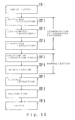
- Figure 10 is a flowchart of the character recognition method in the normalization module 16 using the first principle of this invention.
- a document image is read.
- a histogram is calculated for the read page. This histogram calculation comprises addition to obtain the number of dots on a page projected vertically and horizontally.
- the histograms correspond to respective obliquenesses considered to be within an obliqueness range used for adjusting the obliqueness of the form.
- the obliquenesses of the form obtained from the histograms are respectively adjusted. Since the histograms correspond to the obliquenesses, the difference between the maximum and minimum of the histogram values is maximized when the form is set at the proper position. That is, the obliqueness of the form is determined from the obliqueness that maximizes the difference between the maximum and minimum of the histogram values among those calculated in correspondence with a plurality of obliquenesses.
- the results of adjusting the forms' obliquenesses through histogram calculation are received for finding a character area to be used as a unit for extracting a character.
- the above steps segment the image inputs into areas in character units, so that a character for which a conversion table is created is normalized.
- the conversion table is used for normalizing the extracted characters to a predetermined size by magnifying or contracting them in both directions in one-dot units.
- All the extracted characters, e.g. of M by M dots, in the read document are normalized, e.g. to D by D dots.
- the code of the recognized character is outputted as the result.
- a systolic array is used for expediting the processings, as follows.
- inputted images comprise M by M dots, have two-value images and are to be normalized to a size of D by D dots.
- a normalization is a processing for absorbing the effect of differences in sizes and positions of the character areas of the inputted images by magnifying or contracting the originally inputted images to a predetermined size.
- linear normalization linearly magnifies or contracts the sizes of inputted images to a predetermined size.
- any other normalizations i.e. non-linear normalizations
- line densities the numbers of white elements inverted to black picture elements
- f(i) and g(j) the numbers of white elements inverted to black picture elements
- Conversion functions F(i) and G(j) for mapping are defined as follows. where i s and j s respectively represent the uppermost row and the leftmost column in an area where black picture elements exists, and b which usually is 1 represents a positive weight coefficient for deciding the degree of non-linearity.
- the dots in the columns with fewer inversions from white picture elements to black picture elements are magnified in the row direction by smaller magnification rates, and the dots in the columns with more inversions from white picture elements to black picture elements are magnified in the row direction by larger magnification rates.
- the dots in the rows with fewer inversions from white picture elements to black picture elements are magnified in the column direction by smaller magnification rates, and the dots in the rows with more inversions from white picture elements to black picture elements are magnified in the column direction by larger magnification rates.
- Non-linear normalization is effective for all the embodiments of this invention, in which lines of the character to be recognized are narrowed.
- Figures 11A and 11B show an example of a non-linear normalization in the normalization module 16 using the first principle of this invention. More specifically, Figure 11A shows a character before a non-linear normalization and Figure 11 B shows a character after the non-linear normalization.
- a normalization in the row direction is similarly performed by using F(j) and H, where H is the maximum of F(j) in an area where a black picture element exists.
- Figure 12 illustrates creations of conversion functions in the normalization module 16 using the first principle of this invention.
- Figure 13 shows a loop program for a normalization by the normalization module 16 using the first principle in this invention.
- Figure 14 shows an example of converted data at various stages of a normalization by the normalization module 16 using the first principle of this invention.
- a conversion function realizes a normalization in a procedure cf "normalization in the row direction - ⁇ horizontal conversion - ⁇ normalization in the column direction - ⁇ transposition", as shown in Figure 14. Although a transposition is not described in detail, it is realized by a memory element circuit having an exclusive two-input/output port.
- equation (4) is redundantly rewritten into the following double loop program.
- a loop program shown in Figure 13 is obtained by applying this conversion to equation (3) and rewriting the condition with the conversion function F(i), where it is expressed as an array F[i].
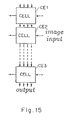
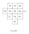
- Figure 15 shows a schematic view of an array in the normalization module 16 using the first principle of this invention.
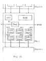
- Figure 16 shows a configuration of a cell in the normalization module 16 using the first principle of this invention.
- a cell has a function of adding and comparing the register values and comprises a logical operation circuit ALU, six (6) registers RE1 through RE6 for storing computed values, one (1) register RI for inputting image data, and a memory circuit RAM for describing a cell function.
- a logical operation circuit ALU six (6) registers RE1 through RE6 for storing computed values
- one (1) register RI for inputting image data
- a memory circuit RAM for describing a cell function.
- four (4) registers RE4, RE5, RE6 and RI are capable of sending a value to a neighboring cell. Names of values memorized in registers at a creation of a conversion function and at a normalization are respectively put in parentheses [ ] and ( ) for describing cell functions.
- the memory circuit RAM stores a microprogram for describing a cell function beforehand. Each cell updates the values of respective registers RE1 through RE6 and RI.
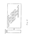
- Figure 17 shows an input sequence of shifted data in the normalization module 16 using the first principle of this invention.
- registers RE1 through RE6 and RI are all set to 0 in a cell initialization.
- the picture element of row i and column (t-i+1 ) of the inputted image is inputted to CELL(i) at time t.
- data shifted by a row are inputted as shown in Figure 17.
- CELL(i) obtains the following values from the loop program shown in Figure 12 and stores them in respective registers RE1 through RE6 and RI.
- the value of b is ordinarily 1 (for a non-linear normalization) or 0 (for a linear normalization).
- Such multiplications as a doubling and a quadrupling can be realized by shifting data without using an adder.
- the value of register RE1 i_img stores all data (of M bits) for row i of the inputted image through a register RI for inputting image data (or directly) and sets the values of registers RE2 and RE3 to the values of D * F(i-1) and D * F(i), respectively.
- the column direction conversion function G(j) is used instead of F(i).
- r_max is the maximum in the row direction obtained at the creation of the conversion function.
- c_max is obtained.
- value acc2 stored in register RE3 in CELL(i) and value acc1 stored in register RE2 in CELL(i+1) are set as F(i) * size+pos, and the value substituted into register RE5 in CELL(1) is described as max.
- the values of pos differ according to the arranged position, and When an adder is not employed, d is limited to an integer exponent of two (2).
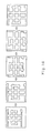
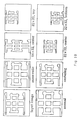
- Figure 18 shows various examples of normalizations of the same character in the normalization module 16 using the first principle of this invention. More specifically, Figure 18 shows an example of an actual performance of the above three (3) kinds of normalizations with the systolic array shown in Figure 16.
- a systolic array for a normalization is applied to an obliqueness adjustment and to a histogram calculation of black picture elements necessary for a character extraction, where data handled are assumed to be two-value images of M by N dots.
- N is equivalent to the horizontal length of inputted image data.
- Figure 19 shows an algorithm for a histogram calculation in the normalization module 16 using the first principle of this invention.
- a histogram is calculated by an algorithm, which is described by the loop program shown in Figure 19. This program is similar to those used in creating conversion functions for normalizations. Cell functions are realized without changing the data inputting method, as follows. Although no other registers are used unless anything but a histogram is calculated, if register RE4 with value r_acc and register RE1 with value c_acc are used and cell functions are defined as it becomes possible to obtain the accumulation value of a histogram in the row and column directions and the number of black picture elements in the entire image. Some algorithms for extracting characters are thought to use these values.
- Figure 20 shows adjustments of obliquenesses in the normalization module 16 using the first principle of this invention.
- register RE1 with value i_img stores data (of K bits) of row i of the inputted image. Data are not inputted.
- CELL(i) has the following cell functions. However, at CELL(1) where t and L represent time and block number, respectively.
- Figure 21 explains the principle of magnification by the row-histogram module 13 and the column-histogram module 14 using the second principle of this invention, which utilizes a systolic array.
- Figure 21 explains the principle for magnification, in which a processing is performed to change the area 0 ⁇ X ⁇ W on the X axis to the area 0 ⁇ Y ⁇ D on the Y axis.
- X and Y are any real numbers
- character width W of the inputted graphic must be determined and histograms in horizontal and vertical directions are created, that is a conversion table is created.
- the column histogram is linear, it is obtained by assigning 1 to the value of the column to which the leftmost point contained in the character area on the image data belongs and by sequentially incrementing the values of the columns to the right by 1.
- the row histogram is linear, it is obtained by assigning 1 to the value of the row to which the uppermost point contained in the character area on the image data belongs and by sequentially incrementing the values of the rows below by 1.
- the conversion table creation module 17 determines the width W of this character and the head ends of the column and the row.
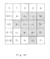
- Figure 22 shows the configurations of the row-histogram module 13 and the column-histogram module 14 using the second principle of this invention, which utilizes a systolic array.
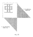
- Figure 23 shows exemplary histograms in the vertical and horizontal directions of the row-histogram module 13 and the column-histogram module 14 using the second principle of this invention, which utilizes a systolic array.
- An image RX extracted by the read control part 15 (Refer to Figure 2A.) is inputted into a histogram generation circuit network (of NA * NA bits) 61 which is for obtaining histograms of the vertical and horizontal directions and the width of the inputted character shown in Figure 23.
- the histograms in the vertical direction is stored in a buffer (of MA * 1 bits) 62 as values in a row unit.
- the histograms in the horizontal direction is directly supplied to a normalization circuit network (of nA * D bits) 64 from the histogram generation circuit network (of NA * NA bits) 61.
- the histogram generation circuit network (of NA * NA bits) 61 has a systolic array structure of NA * NA bits, and image data passing through the histogram generation circuit network (of NA * NA bits) 61 are stored in a buffer (of NA * NA bits) 63. That is, the image RX is finally stored in the buffer (of MA * NA bits) 63.
- the buffer (of MA * NA bits) 63 is not required in this case or could be provided in the normalization module 16.
- the histograms in the vertical and horizontal directions obtained by the histogram generation circuit network (of NA * NA bits) 61 are supplied to and control the operations of the normalization module 16.
- the normalization circuit network (of nA * D bits) 64 is for a normalization in the horizontal direction (in column units).
- a normalization in the vertical direction (in row units) is performed by reading data in dot-row units by a cell structure circuit network (of 1 * D bits) 65 for reading data from the buffer (of MA * NA bits) 63.
- the cell structure circuit network (of 1 * D bits) 65 for reading data performs necessary computations for normalization in the horizontal direction by contemporaneously performing normalization in the vertical direction, and outputs the values and inputted data to the normalization circuit network (of nA*D bits) 64.
- the cell structure circuit network (of 1 * D bits) 65 for reading data reads row i' of the inputted image at time t so that D * h2(i'-1 ) ⁇ tL ⁇ D * h2(i') (8) is satisfied.
- a cell can perform a processing such that while (tL>D * h2(i') && i' ⁇ M) read data && histogram;
- a processing satisfying equation (7) is performed.
- the cell having the value of the histogram in the horizontal direction and column J for calling in the horizontal character width W computes D * h1(j-1), jW and D * h1 (j) and performs conversion such that if D * h1(j') ⁇ jW then j- ⁇ j-1 and if jW ⁇ D * h1(j' -1) then j- ⁇ j+1 where j is a column of the normalized graphic and j' is a column of the inputted graphic.
- the histograms of the inputted character is required for the above normalization.
- the histogram generation is explained further in detail below.
- Figure 24 shows the histogram generation circuit network of the row-histogram module 13 and the column-histogram module 14 using the second principle of this invention, which utilizes a systolic array.
- Respective cells H(1 ,1) through H(Na,Na) comprise a histogram computing cell or a shift register.
- inputted data RX of MA * NA bits are supplied in dot-row units to histogram computing cell H(NA,1) and shift registers H(NA,2) through H(NA,NA).
- An output from histogram computing cell H(NA,1) is supplied to shift register H(NA-1,1), and an output from shift register H(NA,2) is supplied to histogram computing cell H(NA-1,2).
- outputs from shift registers H(NA,3) through H(NA,NA) are supplied to shift registers H(NA-1,3) through H(NA-1,NA).
- histogram computing cells are sequentially provided to the leftmost position in the lowermost row, the second leftmost position in the second lowermost row, the third leftmost position in the third lowermost row, and so forth, to the rightmost position in the uppermost row, and data are sequentially outputted to the next histogram computing cell in this order.
- cell H(NA-1,1) through H(1,1) are provided as shift registers each corresponding to a dot
- cell H(NA,1) is provided as a histogram computing cell.
- the second cell H(NA-1,2) is provided as a histogram computing cell.
- the third cell H(NA-2,3) is provided as a histogram computing cell.
- histogram computing cells are sequentially provided up to the last cell H(1,NA). The respective histogram computing cells sequentially output the results to the next ones right and above in dot units.
- These respective histogram computing cells and shift registers output data to the histogram computing cells and shift registers in the next stages in one clock cycle.
- the shift registers delay received data by one clock cycle.
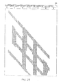
- Figure 25 shows an input sequence shifted data of the row-histogram module 13 and the column-histogram module 14 using the second principle of this invention, which utilizes a systolic array.
- the column histogram in the horizontal direction is obtained by assigning 1 to the value of the column to which the leftmost point contained in the character area on the image data belongs and by sequentially incrementing the values of the columns to the right by 1.
- the character width can be obtained from the histogram value of the rightmost column having a black picture element on the inputted image data, because they are the same.
- the histogram in the vertical direction can be similarly obtained. However, whereas functions are distributed spatially for the histogram in the horizontal direction, they are distributed time-wise for the histogram in the vertical direction.
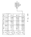
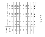
- Figure 26 shows in detail the configuration of a linear histogram computing cell of the row-histogram module 13 and the column histogram 14 module using the second principle of this invention, which utilizes a systolic array.
- a “flag” determines the existence of a black picture element in a scanning
- a "count” is a histogram value
- a "width” is a character width value.
- An “ x “ and a “y” express the vertical direction and the horizontal direction.
- "yflag”, "xwidth” and “xcount” are data sent to the right cell as a result of processing the cell value of the left column.
- "ywidth”, “ycount” and “xflag” are data stored in the respective cells as a result of processing their own cell values.
- "xflag", "xcount” and “xwidth”, as well as “yflag”, "ycount” and “ywidth” are determined by the following expressions.
- the histogram in the horizontal direction, the horizontal character width and the vertical character width are expressed by the values of "xcount”, "xwidth” and "ywidth”, respectively.
- the histogram in the vertical direction is outputted sequentially as the ycount of cell H(1,NA) after time NA.
- Figure 27 shows an exemplary horizontal histogram of the row-histogram module 13 and the column-histogram module 14 using the second principle of this invention, which utilizes a systolic array.
- Figure 28 shows in detail the configuration of a non-linear histogram computing cell of the row-histogram module 13 and the column-histogram module 14 using the second principle of this invention, which utilizes a systolic array.
- a “flag” determines the existence of a black picture element in a scanning
- a "count” is a histogram value
- a “stack” is a value accumulated in the histogram at a row.
- "x” and “y” express the vertical and horizontal directions.
- "yflag”, “xstack” and “ycount” are data sent to the right cell as a result of processing the cell value of the left column.
- "ystack”, “xcount” and “xflag” are data stored in respective cells as a result of processing their own cell values.
- "xflag”, "xcount” and “xstack”, as well as “yflag”, "ycount” and “ystack” are determined by the following expressions.
- the histogram in the horizontal direction finally becomes the example shown in Figure 28, the horizontal and vertical character widths are expressed by the values of "xcount" of cell H(1,NA) and "ycount” of cell H(1,NA), respectively, and the histogram in the vertical direction is sequentially outputted as "ycount" of cell H(1,NA) at and after time NA.
- Figure 29 shows the configuration of the normalization circuit network of the normalization module 16 using the second principle of this invention, which utilizes a systolic array.
- the cell structure circuit network for reading data 65 (Refer to Figure 22.) comprises data reading cells RS1 through RSn and reads data stored in the buffer (of MA * NA bits) 63 in dot-row units after the histogram generation circuit network (of NA * NA bits) 61 creates a histogram.
- the normalization circuit network (of nA * D bits) 64 performs a normalization in the horizontal direction and the cell structure circuit network for reading data 65 performs a normalization in the vertical direction.
- the cell structure circuit network for reading data 65 calculates the value necessary for a normalization in the horizontal direction by concurrently performing the earlier described normalization in the vertical direction and outputs the value and inputted data to the normalization circuit network (of nA * D bits) 64.
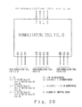
- Figure 30 shows the configuration of normalizing cells P(1,1) through P(D,NA) of the normalization module 16 using the second principle of this invention, which utilizes a systolic array.
- Representative normalizing cell P(i,j) receives data t2, u2, l2 and e2 from corresponding normalizing cell P(i+1,j) in the prior state. P(i,j) also receives data u1 , l1 and e1 from normalizing cell P(i+1,j-1), which neighbors to corresponding cell P(i+1,j), as well as u3, l3 and e3 from another normalizing cell P(i+1,j+1), which neighbors and is opposite to corresponding cell P(i+1,j). Each normalizing cell P(i,j) calculates data t, u, l and e from the inputs described earlier and supplies the data to a normalizing cell P(i-1,j) in the posterior stage. This normalizing cell P(i,j) performs the processings shown in Figure 30. That is, they are expressed as follows.
- the obtained resultant data t,u, l and e are outputted to normalizing cell P(i-1,j) and neighboring normalizing cells P(i-1,j-1) and P(i-1,j+1) in the posterior stage.
- the normalization circuit network (of nA * D bits) 64 processes a normalization in the horizontal direction.
- the number of stages in the horizontal direction of the normalization circuit network (of nA * D bits) 64 described earlier corresponds to the numbers of bits n1 and n2 to be expanded to the left and right, as shown in Figure 22. In other words, it is the greater value of the left and right margins n1 and n2 of the inputted data. That is, it is enough to input the maximum value of the dot width of the character input.
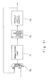
- Figure 31 shows the configuration of the normalization module 16 using the third principle of this invention.
- a circuit configured as shown in Figure 31 enables a normalization, other than a normalization by a systolic array described earlier.
- Image data to be contracted or magnified are supplied to terminal A in dot-column units or in dot-row units.
- a selection circuit 70 outputs image data supplied from terminal A to a normalization part 71 by selecting them per the instruction from a control circuit not shown in the drawing.
- the normalization part 71 normalizes parallelly supplied dot data in the vertical direction.
- Figure 33 illustrates the principle of the normalization module 16 using the third principle of this invention.
- the normalization part 71 reads and contracts data sequentially supplied in dot-column units in the vertical direction.
- the 128 dots by 128 dots are contracted, e.g. to 64 dots by 64 dots, to change one of the two sides to 64 dots (a primary conversion)
- data of a plurality of dot columns (two dot columns in this case) read in 128 dot units are "OR" added to be outputted as a single dot column.
- Normalized data outputted from the normalization part 71 (At this time, the dot number of one dot column does not change.) are supplied to a parallel-to-serial conversion circuit 72 (P/S) to be converted to serial data which are supplied to a variable length register 73.
- P/S parallel-to-serial conversion circuit 72
- variable length register 73 supplies the serial data of 128 dots in a first register.
- Parallel data of 128 dots of the second column are supplied to a second register.
- variable length register 73 comprises a plurality of variable-length shift registers.
- serial data of 128 dots are supplied sixty-four (64) times to the variable length register 73.
- FIGS 35A and 35B explain in detail operations of the normalization module 16 using the third principle of this invention.
- variable length register 73 After the primary conversion is completed, the variable length register 73 outputs the result, which is supplied to terminal B of the selection circuit 70 that in turn selects and inputs data supplied to terminal B to the normalization part 71 per an instruction from a control circuit not shown in the drawing.
- variable length register 73 Since the variable length register 73 outputs head end dots respectively supplied in dot units from the parallel-to-serial conversion circuit 72, the variable length register 73 for memorizing data which have undergone the primary conversion from 128 dots by 128 dots as shown in Figure 33 outputs the data in a 64 dot unit.
- the normalization part 71 contracts the character represented by the 64-dot data supplied a total of 128 times, e.g. to one represented by 64 dots by 64 dots.
- the operations of the normalization part 71 are similar to the normalizing operations described earlier.
- data of 64 bits are parallelly received to be outputted by a plurality of "OR" additions to be contracted before they are outputted to the parallel-to-serial conversion circuit 72, which in turn converts them to serial data to be inputted to the variable length register 73.
- the normalization part 71 receives 128 pairs of 64-dot data in parallel, since the normalization part 71 contracts them in the direction along the 128 pairs, the result obtained from the normalization part 71 after the secondary conversion is of 64 dots by 64 dots.
- the data which have undergone the secondary conversion are converted to serial data by the parallel-to-serial conversion circuit 72.
- the serial data of 64 dots by 64 dots are supplied to the variable length register 73 to be memorized and outputted to the next processing, e.g. at the line-narrowing module 18.
- Figure 32 shows in more detail the configuration of the normalizing part 71 in the normalization module 16 using the third principle of this invention. Circuits in Figure 32 the same as those in Figure 31 have the same numbers, and their explanations are saved.
- the normalization part 71 comprises an "AND” gate 81, an "OR” gate 82 and a flip-flop 83.
- One of the inputs of the "AND” gate 81 is supplied with a gate control signal from a control circuit not shown in the drawing.
- a contraction requires an "OR” addition.
- an H signal for turning on the "AND” gate 81 is applied from outside.
- the "AND” gate 81 inputs data memorized in the flip-flop 83 to the "OR” gate 82. That is, the flip-flop 83 re-inputs data routed through the "AND” gate 81 and the "OR” gate 82 which the flip-flop 83 originally memorized by itself.
- the "AND” gate 81 performs the "OR" addition.
- Contracted data memorized in the flip-flop 83 are received in the parallel-to-serial conversion circuit 72 per an instruction by a receiving signal from a control circuit not shown in the drawing. A magnification or a contraction is performed in accordance with the sequence wherewith the receiving signal is supplied.
- the conversion table creation module 17 shown in Figure 2A is a circuit for creating a conversion table, indicating the relation between a variable I and a conversion table function value H(I), to obtain a receiving position in a magnification or a contraction.
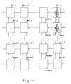
- Figure 34 explains the operations of the normalization part 71 in the normalization module 16 using the third principle of this invention.
- FIGS 35A and 35B explain in detail the operations of the normalization module using the third principle of this invention.
- the normalization part 71 obtains a conversion table value H(I) * D by sequentially incrementing I by 1 from the initial value 1. Initially, i.e. when i is 1, the value H(1) * D is obtained by multiplying H(1) by the dot number D to be changed. Since H(1) is 0, H(1) * D is also 0.
- the normalization part 71 sequentially compares H(I) * D with SIGMA[W] by incrementing variable J by 1.
- a character is normalized by the result obtained in the conversion table creation module 17 through the above operations.
- the comparisons are then performed with the character width W obtained simultaneously at the conversion table creation module 17 as described earlier.
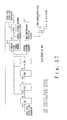
- Figure 36 shows in detail the system configuration of the normalization module 16 using the third principle of this invention.
- an instruction of a system CPU is supplied to each module by a system bus SBUS comprising a control bus, an address bus, and a data bus.
- a system bus SBUS comprising a control bus, an address bus, and a data bus.
- Each module is provided with a local CPU 140 which exchanges data with the system bus SBUS through a bus arbiter (ARB) 141.
- ARB bus arbiter
- the system bus SBUS is connected to the local CPU 140 through the bus arbiter (ARB) 141.
- a local bus of the local CPU 140 is connected not only to the bus arbiter (ARB) 141 but also to a data memory 144 through a memory 142 and a bus transceiver 143.
- the data memory 144 is connected to the system bus SBUS through a bus transceiver 145 so that data can be accessed in response to an access from the local CPU 140, as well as from the system CPU through the bus transceiver 145.
- the local CPU 140 executes a program stored beforehand in ROM in the memory 142 to control the module operations.
- the local CPU 140 is connected to the system bus SBUS described earlier through the bus arbiter (ARB) 141, as well as to a module bus 146 comprising an address bus and a data bus.
- the module bus 146 is connected to a FIFO character buffer 153 through a two-port SRAM 147, a common RAM 148, a normalization size register 150, a row/column maximum value register 151 and a bus transceiver 152.
- the two-port SRAM 147 which is a memory register is connected to an ID bus of the conversion table creation module 17, and upon receiving various information the two-port SRAM 147 notifies the local CPU 140 that the information is inputted, by interrupting the local CPU 140.
- data stored in the FIFO character buffer 153 are supplied through a buffer 155 to parallel-to-serial conversion circuits (ALTI, P/S) 156 and 157.
- the buffer 155 outputs 16-bit data in 128 bit-units by sequentially memorizing eight (8) words (128 bits) of character pattern data inputted from the FIFO character buffer 153 and supplies them simultaneously to the parallel-to-serial conversion circuits (ALTI, P/S) 156 and 157 in 64-bit units.
- a clock instructing the parallel-to-serial conversion circuits (ALTI, P/S) 156 and 157 to receive 64-bit data is not shown in the drawing, a clock pulse of such a clock is supplied from a comparator 159. Each time a "big" signal for indicating big data is supplied from the comparator 159, the parallel-to-serial conversion circuits (ALTI, P/S) 156 and 157 receive 64-bit data.
- An accumulator 158 accumulates the row/column maximum value W outputted from the row/column maximum value register 151 to output the result to the comparator 159.
- the FIFO conversion table 149 memorizes a conversion table function value H(I) and supplies it to a barrel shifter 160. Meanwhile, a normalization size value D (7-bit data), by which H(I) is multiplied, is inputted to a decoder (DEC) 161 to be decoded.
- DEC decoder
- the decoder DEC 161 decodes the conversion sizes into n by taking their exponents. Since the barrel shifter 160 shifts H(I) inputted from the FIFO conversion table 149 by the decoded value n, a multiplication of 2 n *H(I) is performed and the result is inputted to the comparator 159, which is a circuit for comparing the value supplied from the barrel shifter 160 with the value supplied from the accumulator 158.
- the comparator 159 instructs the consecutive parallel-to-serial conversion circuits (ALTI, P/S) 156 and 157 to receive 128-bit data memorized in the buffer 155.
- the local CPU 140 controls the execution state and the result.
- variable length registers 162, 162', 163 and 163' are shift registers each of 32 dots * 64 dots and are inputted with 64-bit serial data in units of 64-bit columns. For instance, in the primary conversion for the first row, the variable length registers 162 and 163 operate to simultaneously receive 128-bit data in 64-bit units.
- the local CPU 140 judges that the variable length registers 162, 162', 163 and 163' store data and complete the operations of the primary conversion, the local CPU 140 causes the parallel-to-serial conversion circuits (ALTI, P/S) 156 and 157 to supply two 32-bit data respectively to the variable length registers 162 and 162' and the variable length registers 163 and 163'. That is, that the variable length registers 162, 162', 163 and 163' sequentially re-input 64-bit data from the head end of the 64 pairs of serial data inputted from the parallel-to-serial conversion circuits (ALTI, P/S) 156 and 157.
- the parallel-to-serial conversion circuits (ALTI, P/S) 156 and 157 sequentially re-input 64-bit data from the head end of the 64 pairs of serial data inputted from the parallel-to-serial conversion circuits (ALTI, P/S) 156 and 157.
- the output from the parallel-to-serial conversion circuits (ALTI, P/S) 156 and 157 are supplied through the variable length registers 162 and 163 to the normalized image FIFO buffer 165 as parallel data after the conversion.
- the parallel-to-serial conversion circuits (ALTI, P/S) 156 and 157 comprise an ALTI
- the parallel output could be similarly supplied to the variable length registers 162, 162', 163 and 163', by providing a support for a parallel output from the local CPU 140.
- Data contracted by the above procedures are memorized in the normalized image FIFO buffer 165 and image data after a normalization are supplied to the line-narrowing module 18 e.g. through an ID bus or through a buffer 166 and the personal bus 154.
- the input parts of the parallel-to-serial conversion circuits (ALTI, P/S) 156 and 157 are provided with "OR" addition circuits for receiving the results of "OR” adding the inputted data.
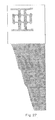
- Figure 37 shows in detail the configuration of the line-narrowing module 18 using the first principle of this invention.
- Image data before a line is narrowed are supplied sequentially to a shift register SR1 by vertically read in 3-dot units comprising the center dot of the line to be narrowed and the dots to its left and right.
- Data memorized in the shift register SR1 are sequentially shifted to shift registers SR2, SR3 and SR4 after each time one clock cycle elapses.
- These shift registers SR1 through SR4 memorize in four stages a total of 11 bits of dot data.
- These memorized dot data are supplied to an address of a conversion table memory M1 for memorizing information that makes a black center dot of the 3*3+2 dots white when the dots around the center dot are of a particular pattern.
- the center dot corresponding to the inputted dot data is determined (converted) by the information.
- the converted data DA are supplied to a FIFO F1 (or to a line-narrowing circuit in the next stage).
- the shift registers SR1 through SR4, and the FIFO F1 receive the center dot and the dots to its left and right, and the dots above and below it are supplied for one character or one document.
- a non-conformance detection circuit S1 compares the center picture element supplied to the address of the conversion table memory M1 with the converted data DA for the center picture element, and supplies a non-conformance signal to a JK flip-flop F2 when a non-conformance has arisen. On receipt of the non-conformance signal, the JK flip-flop F2 memorizes it.
- a CPU controls the circuits shown in Figure 37.
- the JK flip-flop F2 memorizes it.
- the CPU considers that there are points to be changed by a series of converting operations in the area of the line to be narrowed.
- the CPU does not receive the data after line-narrowing outputted from the FIFO F1, but repeats the control operations described earlier. At this time, the CPU resets the flag of the JK flip-flop F2.
- the JK flip-flop F2 receives no data and a non-conformance flag is not outputted. When the flag is not outputted, data of the previous time and data after the conversion are matched. The CPU considers this as a conversion termination and receives data from the FIFO F1.
- Figure 38 illustrates the operation of the conversion in the line-narrowing module 18 using the first principle of this invention.
- Shift registers SR1, SR2, SR3 and SR4 receive 3-bit, 4-bit, 4-bit and 3-bit inputs, respectively. Thus, a total of fourteen (14) bits are memorized. However, only eleven (11) of the fourteen (14) bits memorized are actually supplied to addresses A0A through A10A in the conversion table memory M1.
- shift register SR1 Of the three (3) bits memorized in shift register SR1, one (1) is supplied to address A9A. Of the four (4) bits memorized in shift register SR2, three (3) are supplied to addresses A0A, A1A and A2A. All four (4) bits memorized in shift register SR3 are supplied to addresses A10A, A3A, A4A and A5A.
- the center picture element of the conversion table memory M1 is in address A4.
- the conversion table memory M1 memorizes a determinant for determining whether or not the center picture element is changed per bit data stored in the surrounding addresses and outputs a converted one-bit center picture element.
- Figure 39 is a flowchart of operations of a CPU for controlling the line-narrowing module 18 using the first principle of this invention.
- the CPU resets the non-conformance flag.
- the CPU starts controlling for receiving the image scanning data stored e.g. in an external device.
- the CPU judges whether or not all image scanning data for one character are completely received. If it judges that all the image scanning data are not received (N), STEP 12 is repeated. If it judges that all the image scanning data are received (Y), STEP 14 is invoked.
- the CPU judges whether or not the non-conformance flag is on. If the non-conformance flag is on (Y), STEP 15 is initiated. If the non-conformance flag is not on (N), STEP 18 is invoked.
- the CPU judges whether or not the loop processings from STEP 11 through STEP 14 have been performed a predetermined number of times. If the CPU judges they have (Y), STEP 16 is invoked. If the CPU judges they have not (N), STEP 11 is repeated.
- the CPU determines that the line scanning data represents a different character, because line-narrowing has not yet been completed.
- a line-narrowing table conversion is performed in consideration of the possibility of another character. After the processing in STEP 17 has been performed, STEP 11 is repeated.
- the image scanning data at this time are processed by the data stored in the FIFO F1. After repeating the above operations, when the non-conformance flag is not on (N) in STEP 14, the line-narrowing processings are terminated.
- the conversion table memory M1 a RAM, is connected to the CPU.
- the CPU performs a new line-narrowing by accessing the conversion table in the conversion table memory M1.
- a line is narrowed in the input direction of one-column dot data, i.e. in the vertical direction, into a line comprising one dot left and right.
- a line is narrowed by performing these operations a plurality of times for the number of columns of the inputted character. For example, if the inputted character comprises 64 dots by 64 dots, the above procedures are repeated 64 times.
- a line is narrowed in dot-row units in the operations described in Figures 37, 38 and 39
- a plurality of lines narrowed in dot-row units are provided in the column direction in these embodiments of this invention, so that e.g. 64-bit data for a row of a character are processed in parallel.
- Figure 40 shows in detail the configuration of the line-narrowing module 18 using the first principle of this invention.
- Inputted data are stored in a FIFO F3.
- 64-bit data for a dot row of a character comprising 64 dots by 64 dots are supplied parallelly.
- the FIFO F3 is e.g. a shift register of 64 stages.
- Data memorized in the FIFO F3 are supplied to shift register SR1NC through a buffer B1. Its output is supplied to shift register SR1NC. Its output is in turn supplied to shift register SR2NC. Then its output is supplied to shift register SR3NC. Finally its output is supplied to shift register SR4NC.
- Shift registers SR1NC through SR4NC receive clock signals from a sequencer SC and shift data from the buffer B1 in correspondence with the clock signals.
- a total of 4NC pieces of data stored in shift registers SR1NC through SR4NC are supplied to a conversion table memory MNC which comprises (NC-2) pieces of memories for memorizing the same converted data, and determines the center from the center dot datum.
- the eight (8) surrounding dots, the dot two up and the dot two to the left are supplied to the respective memories.
- Figure 41 illustrates in detail the operations of the line-narrowing module 18 using the first principle of this invention.
- shift registers SR1NC SR2NC, SR3NC and SR4NC then memorize data E1 through ENC, data D1 through D(3NC-2), data D2 through D(3NC-1) and data D3 through D3NC, respectively.
- the conversion table memory MNC comprises RAM0 through RAM(NC-1) which receive data at their address terminals.
- RAM0 stores data E1 and D1 through D6, and its center datum is D2.
- RAM1 stores data E2 and D1 through D9.
- RAM2 stores data E3, D2 and D4 through D12, and its center datum is D5, and its center datum is D8.
- Other RAM's store data similarly.
- RAM(NC-2) stores data E(NC-1), D(3NC-10) and D(3NC-8) through D3NC, and its center datum is D(3NC-4).
- RAM(NC-1) stores data EN, and D(3NC-7) through D(3NC-3), and its center datum is D(3NC-4).
- Respective data are inputted to RAM0 through RAM(NC-1) at their proper addresses, as shown in Figure 41.
- the results of conversion at RAM0 through RAM (NC-1) are supplied to a FIFO F4 whose output is supplied again to shift register SR1 through a buffer B2.
- NC pieces of memories RAM0 through RAM(NC-1) narrow lines.
- RAM0, RAM1 and RAM(NC-1) unlike all the other memories RAM2 through RAM(NC-2), have empty dots (outside of the 64 dots), data supplied to the address terminals of those empty dots are set to 0, so that lines at edge parts can be similarly narrowed.
- by adding two dots to make data of 66 dots lines at edge parts can be similarly narrowed.
- the CPU When the CPU starts to control the processing of image data of one character memorized in the FIFO F3, the CPU activates the buffer B1 and the sequencer SC, thereby sequentially inputting data in the FIFO F3 to shift register SR1NC.
- the inputted data are converted by the operations illustrated in Figure 40.
- the converted data are then supplied to the FIFO F4.
- the CPU After the FIFO F4 stores the converted data for one character, the CPU performs a control such that the buffer B2 is activated and the buffer B1 is deactivated, so that the data in the FIFO F4 are supplied again to shift register SR1NC.
- a non-conformance detection circuit S2 compares NC bits of center data of the 4NC bits of data supplied to the conversion table memory MNC with NC bits of its output to determine whether or not they match with each other. When a non-conformance is detected, the non-conformance detection circuit S2 supplies a non-conformance signal to a JK flip-flop F5 to set it.
- the CPU again controls the execution of a conversion processing, by judging that a non-conformance exists, i.e. that a conversion has been performed and a change has been made.
- the CPU again resets the JK flip-flop F5 to a processing condition.
- the sequencer SC being terminated is reactivated.
- the JK flip-flop F5 When a non-conformance is not detected, the JK flip-flop F5 is not set.
- the CPU judges that no change has been made and reads the conversion data stored in the FIFO F4.
- the data are a collection of narrowed lines whose widths are e.g. one dot.
- Figure 42 shows the configuration of the non-conformance detection circuit in the line-narrowing module 18 using the first principle of this invention.
- the bit number NC described in Figures 40 and 41 is 64.
- the non-conformance detection circuit S2 compares bits respectively supplied bit-by-bit from NC-bit ports A and B, as shown in Figure 42. That is, to judge whether or not they agree, the non-conformance detection circuit S2 supplies the compared bits to exclusive logical "OR” gates EOR1 through EOR(NC-2) whose outputs are in turn supplied to an "OR" gate 170.
- the non-conformance detection circuit S2 determines whether they conform with each other, depending on the output from the "OR” gate 170.
- Exclusive logical "OR” gates EOR1 through EOR(NC-2) output 0 when the compared bits agree with each other, and 1 when they don't.
- the "OR” gate 170 outputs a non-conformance, i.e. an "H" level.
- a non-conformance flag is set in the JK flip-flop F5, and the CPU determines whether or not line-narrowing should again be executed by judging the non-conformance.
- a clock signal indicating a conformance is supplied to the JK flip-flop F5 described earlier.
- the JK flip-flop F5 receives the output from the non-conformance detection circuit S2 upon receiving this clock signal.
- Figure 43 shows the configuration of the line-narrowing module 18 using the first principle of this invention.
- line-narrowing is not limited to sequential processings.
- pairs of line-narrowing circuits SXC1, SXC2, etc. each comprising a plurality of stages for the line-narrowing amount (determined by the thickest line inputted) are provided for a pipeline processing that enables even faster line-narrowing.
- Figure 44 shows the configuration of a line-narrowing array in the line-narrowing module 18 using the second principle of this invention, which uses a systolic array.
- the line-narrowing illustrated in Figures 37 through 43 is performed by processings in one-dot units or in parallel.
- the following processing uses an array.
- Data in a character frame normalized by the normalization module 16 are supplied in dot-row units to the line-narrowing module 18, which comprises line-narrowing cells M(1,1) through M(L,ND).
- Respective line-narrowing cells M(1,1) through M(L,ND) output two bits to the above cell and input one bit from the above cell.
- Figure 45 shows in detail the configuration of line-narrowing cells M(1,1) through M(L,ND) in the line-narrowing module 18 using the second principle of this invention, which uses a systolic array.
- shift register RS11 which is a four-stage shift register comprising registers R10, R2, R8 and R6.
- the data D0 are also supplied to the neighboring cells below. Meanwhile, data supplied from the neighboring cell below are supplied to shift registers RS12 and RS13.
- shift register RS12 data from an upper cell are supplied to shift register RS12, and data from a lower cell are supplied to shift register RS13.
- Shift register RS12 comprises registers R3, R4 and R5.
- Shift register RS13 comprises registers R1, R0 and R7.
- data supplied from a lower cell are supplied to register R9.
- Outputs from register R7 are supplied to register R0, as well as to an upper cell in Figure 45. That is, register R9 is supplied with data shifted by one stage in the lower cell in Figure 45.
- Figure 46 illustrates the pattern positions of the registers in the line-narrowing module 18 using the second principle of this invention, which uses a systolic array.
- the data D0 inputted to each cell comprises one (1) dot in register R8, eight (8) dots in eight (8) registers R0 through R7 around register R8, one (1) dot in register R10 two to the left of register R8, and one (1) dot in register R9 two down from register R8, i.e. a total of eleven (11) dots.
- memory F sets the value of data D11 or data D12 to 1.
- Data D11 and D12 are supplied to "AND" gates 183 and 184. As described earlier, if the value of the center dot stored in register R8 is determined, the values of data D11 and D12 are 0; if it is not determined, the value is obtained by considering two other dot values.
- the data D11 and D12 act as instruction signals for determining output data obtained as a result of considering the dot values stored in registers R10 and R9.
- Outputs from register R10 are supplied through an inverter 182 to an "AND” gate 183.
- Outputs from register R9 are supplied through an inverter 185 to an "AND” gate 184.
- the value of data D11 is 1, the dot data value stored in register R10 is inverted, and the result determines the output.
- the value of data D12 is 1, the value outputted from register R9 determines the output.
- the outputs from the "AND” gates 183 and 184 are supplied to an "OR” gate 181. If either of the outputs is 1, the "OR” gate 181 outputs 1.
- the output from the "OR” gate 181 is supplied to an "OR” gate 180. Accordingly, the output data D20 represent the logical outputs from "AND” gates 183 and 184. That is, when the data stored in register R8 is set as the center dot value and the center dot value is not determined by the surrounding data (memorized in registers R0 through R7), the value stored in register R9 or R10 determines it.
- Figure 47 is an input data diagram in the line-narrowing module 18 using the second principle of this invention, which uses a systolic array.
- Figure 48 illustrates data change in the register of the input data in the line-narrowing module 18 using the second principle of this invention, which uses a systolic array.
- data A1, B1, C1 and D1 are supplied respectively to cells J+1 , J, J-1 and J-2.
- Shift registers RS11, RS12 and RS13 in cell J respectively store data B1 , A1 and C1.
- Shift registers RS11, RS12 and RS13 in cell J-1 respectively store data C1, B1 and D1.
- Register R9 in cell J stores a void datum.
- shift registers RS11, RS12 and RS13 in cell J respectively store data B1 and F1, A1 and E1, C1 and G1.
- Register R9 in cell J stores datum D1.
- Shift registers RS11, RS12 and RS13 in cell J respectively store data B1, F1 and J1; A1, E1 and I1; C1, G1 and K1.
- Register R9 in cell J stores datum H1.
- Shift registers RS11, RS12 and RS13 in cell J respectively store data B1, F1 J1 and N1; E1, I1 and M1 and; G1, K1 and O1.
- Register R9 in cell J stores datum L1.
- Figure 49 shows the configuration of the stroking array in the stroking module 19 in the embodiment of this invention using an array.
- Figure 50 shows the configuration of a stroking cell in the stroking module 19 in the embodiment of this invention using an array.
- Dot data for a character obtained at the line-narrowing module 18 are supplied to stroking cells SX1 through SXNE. That is, data D1 through DNE forming a dot row are respectively supplied to stroking cells SX1 through SXNE.
- the stroking cells SX1 through SXNE simultaneously output the supplied data D1 through DNE to the neighboring cells.
- the stroking cell SX2 simultaneously outputs data inputted to the stroking cells SX1 and SX3.
- each stroking cell is supplied from the neighboring cells with dots neighboring the dot of the corresponding position.
- respective stroking cells SX1 through SXNE comprise three shift registers SR-C, SR-R, SR-L, and dots supplied from the line-narrowing module 18 are inputted one dot at a time to shift register SR-C as well as shift to registers SR-R and SR-L in the neighboring cells.
- shift register SR-C receives the dot datum corresponding to the cell
- shift register SR-R receives the dot datum to the right of the center cell
- shift register SR-L receives the dot datum to the left of the center cell.
- shift registers SR-L, SR-C and SR-R store data A3B, A4B and A5B in the first dot row; data A2B, A8B and A6B in the second dot row; and then data A1B, A0B and A5B in the third dot row.
- Figure 51 shows a matrix of shift registers in the stroking module 19 in the embodiment of this invention using an array.
- the first, second and third lines of the stroking cell are respectively supplied with data A3B, A4B and A5b; A2B, A8B and A6B; and A1B, A0B and A7B.
- Figure 52 illustrates the operations in the stroking module 19 in the embodiment of this invention using an array.
- a stroking cell SXM supplied with data DM receives its neighboring dots D(M-1) and D(M+1) through stroking cells SX(M-1) and SX(M+1). Therefore, shift register SR-C in the stroking cell SXM supplied with dot DM memorizes data DM1, DM2 and DM3. Shift register SR-R for the right dot stores data D(M+1)1, D(M+1)2 and D(M+1)3. Shift register SR-L for the left dot stores data D(M-1)1, D(M-1)2 and D(M-1)3.
- Shift register SR-C in the stroking cell supplied with data D(M+1) stores data D(M+1)1, D(M+1)2 and D(M+1)3.
- Shift register SR-L stores data DM1, DM2 and DM3.
- Shift register SR-R stores data D(M+2)1, D(M+2)2 and D(M+2)3.
- shift registers SR-C, SR-R and SR-L store a total of 3*3 dot data corresponding to the stroking cell comprising a center dot and surrounding dots above, below, right and left.
- Shift registers SR-C, SR-L and SR-R supply the data to addresses of memory M1 which output 3-bit data corresponding to the pattern and memorized in advance.
- Figure 53 is a stroking table representing shift register values and an output in the stroking module 19 in the embodiment of this invention using an array.
- A0B through A8B in the drawing refer to addresses corresponding to the 3*3 dot data described earlier.
- the values of data A8B and data A4B are both "1"
- the output is set to "010”.
- the value of data A8B and A6B are "1" and the value of data A4B is "0”
- the direction of the stroke is judged to be horizontal, and the output DX is set to "111".
- data coded by respective 3*3 patterns are outputted from stroking cells SX1 through SXNE. Since stroking cells SX1 and SXNE are at the edges, terminals of SX1 and SXNE, not shown, are supplied with "0".
- the respective stroking cells are provided with tables, and neighboring dots are added in cell units, each time one dot row is added in the line direction in the 3*3 dot pattern in a column or row unit, the dot unit is obtained.
- Figure 54 is a noise reduction table in the stroking module 19 in the embodiment of this invention using an array.
- the noise reduction module 11 shown in Figure 2A is configured.
- the present embodiment of this invention is explained for its application to image data, but the application of this invention is not limited to image data, but can be similarly applied to other two-dimensional data in finding their interrelations.
Landscapes
- Engineering & Computer Science (AREA)
- Computer Vision & Pattern Recognition (AREA)
- Physics & Mathematics (AREA)
- General Physics & Mathematics (AREA)
- Multimedia (AREA)
- Theoretical Computer Science (AREA)
- Character Input (AREA)
- Character Discrimination (AREA)
Applications Claiming Priority (15)
| Application Number | Priority Date | Filing Date | Title |
|---|---|---|---|
| JP8421/90 | 1990-01-19 | ||
| JP8420/90 | 1990-01-19 | ||
| JP2008421A JPH03214283A (ja) | 1990-01-19 | 1990-01-19 | シストリックアレイによる変換表作成回路 |
| JP2008420A JPH03214282A (ja) | 1990-01-19 | 1990-01-19 | シストリックアレイによる正規化方式 |
| JP842190 | 1990-01-19 | ||
| JP842090 | 1990-01-19 | ||
| JP33992/90 | 1990-02-16 | ||
| JP2033992A JPH03240175A (ja) | 1990-02-16 | 1990-02-16 | ヒストグラム計算回路 |
| JP3399290 | 1990-02-16 | ||
| JP2058043A JPH03260885A (ja) | 1990-03-12 | 1990-03-12 | 高速文字認識前処理用シストリックアレイ |
| JP5804390 | 1990-03-12 | ||
| JP58043/90 | 1990-03-12 | ||
| JP2066832A JPH03268087A (ja) | 1990-03-19 | 1990-03-19 | イメージデータ正規化回路 |
| JP6683290 | 1990-03-19 | ||
| JP66832/90 | 1990-03-19 |
Publications (3)
| Publication Number | Publication Date |
|---|---|
| EP0447751A2 true EP0447751A2 (fr) | 1991-09-25 |
| EP0447751A3 EP0447751A3 (en) | 1993-06-16 |
| EP0447751B1 EP0447751B1 (fr) | 1999-06-09 |
Family
ID=27518943
Family Applications (1)
| Application Number | Title | Priority Date | Filing Date |
|---|---|---|---|
| EP91100646A Expired - Lifetime EP0447751B1 (fr) | 1990-01-19 | 1991-01-21 | Système de traitment d'image |
Country Status (4)
| Country | Link |
|---|---|
| US (1) | US5436982A (fr) |
| EP (1) | EP0447751B1 (fr) |
| CA (1) | CA2034617C (fr) |
| DE (1) | DE69131304T2 (fr) |
Families Citing this family (2)
| Publication number | Priority date | Publication date | Assignee | Title |
|---|---|---|---|---|
| US6539115B2 (en) * | 1997-02-12 | 2003-03-25 | Fujitsu Limited | Pattern recognition device for performing classification using a candidate table and method thereof |
| US8549496B2 (en) | 2009-02-27 | 2013-10-01 | Texas Tech University System | Method, apparatus and computer program product for automatically generating a computer program using consume, simplify and produce semantics with normalize, transpose and distribute operations |
Family Cites Families (10)
| Publication number | Priority date | Publication date | Assignee | Title |
|---|---|---|---|---|
| US3644890A (en) * | 1969-12-29 | 1972-02-22 | Philco Ford Corp | Optical character recognition system using parallel different scan signal processors to feed higher speed asynchronous recognition register |
| US4656664A (en) * | 1984-10-24 | 1987-04-07 | International Business Machines Corporation | Method for reducing a binary image |
| JPH0731714B2 (ja) * | 1986-05-29 | 1995-04-10 | インタ−ナショナル ビジネス マシ−ンズ コ−ポレ−ション | 文字成分切出し方法 |
| JPH0773920B2 (ja) * | 1986-11-17 | 1995-08-09 | 日本電気株式会社 | n×nビットドットマトリックス90゜回転回路 |
| JPS63261486A (ja) * | 1987-04-20 | 1988-10-28 | Nec Corp | 書体識別装置 |
| FR2623310B1 (fr) * | 1987-11-16 | 1990-02-16 | Commissariat Energie Atomique | Dispositif de traitement de donnees relatives a des elements d'image |
| JPH01245361A (ja) * | 1988-03-28 | 1989-09-29 | Mitsubishi Electric Corp | 画像処理装置 |
| US4958378A (en) * | 1989-04-26 | 1990-09-18 | Sun Microsystems, Inc. | Method and apparatus for detecting changes in raster data |
| JPH077256B2 (ja) * | 1990-07-25 | 1995-01-30 | インターナシヨナル・ビジネス・マシーンズ・コーポレーシヨン | グレイ・スケール・パターンの発生方法 |
| US5063385A (en) * | 1991-04-12 | 1991-11-05 | The United States Of America As Represented By The Secretary Of The Air Force | Radar warning receiver compressed memory histogrammer |
-
1991
- 1991-01-21 EP EP91100646A patent/EP0447751B1/fr not_active Expired - Lifetime
- 1991-01-21 CA CA002034617A patent/CA2034617C/fr not_active Expired - Fee Related
- 1991-01-21 DE DE69131304T patent/DE69131304T2/de not_active Expired - Fee Related
- 1991-01-22 US US07/644,360 patent/US5436982A/en not_active Expired - Lifetime
Also Published As
| Publication number | Publication date |
|---|---|
| EP0447751A3 (en) | 1993-06-16 |
| CA2034617C (fr) | 1996-12-31 |
| EP0447751B1 (fr) | 1999-06-09 |
| DE69131304T2 (de) | 1999-11-11 |
| CA2034617A1 (fr) | 1991-07-20 |
| US5436982A (en) | 1995-07-25 |
| DE69131304D1 (de) | 1999-07-15 |
Similar Documents
| Publication | Publication Date | Title |
|---|---|---|
| US4153897A (en) | Method and device for detecting the similarity between standard and unknown patterns | |
| US5214717A (en) | Pattern recognition data processing device using an associative matching method | |
| US5740285A (en) | Image reduction/enlargement technique | |
| US5016001A (en) | Pattern data generating system | |
| US5832138A (en) | Image processing method and apparatus for extracting lines from an image by using the Hough transform | |
| US4484347A (en) | Method of image transformation in a display device | |
| EP0471482A2 (fr) | Procédé pour le traitement de caractère | |
| JPH0650539B2 (ja) | 文字認識用計算ネットワーク | |
| GB2190778A (en) | Character recognition with variable subdivision of a character region | |
| EP0143533B1 (fr) | Méthode et appareil d'expansion et/ou contraction de données d'image | |
| US5809180A (en) | Data conversion system for line-narrowing a pattern | |
| JP2002230551A (ja) | 確率密度関数を用いたパターン認識装置および方法 | |
| US5436982A (en) | Data processing system | |
| JP2828592B2 (ja) | カーニング処理方法 | |
| US5023920A (en) | Method for finding the medial axis transform of an image | |
| US20190171894A1 (en) | Method and apparatus for determining summation of pixel characteristics for rectangular region of digital image avoiding non-aligned loads using multiple copies of input data | |
| US6938064B1 (en) | Method for computing fast Fourier transform and inverse fast Fourier transform | |
| JP3673598B2 (ja) | 画像処理方法及び画像処理装置 | |
| CN115526858A (zh) | 接线端子检测识别方法、装置、计算机设备、存储介质 | |
| EP0365878A2 (fr) | Méthode de traitement d'image | |
| CN119516279B (zh) | 一种基于多示例迁移学习的图像分类方法、装置、设备及介质 | |
| JPH04311254A (ja) | ニューラル・ネットワーク及びその制御方法及びニューラル・ネットワーク用演算装置 | |
| JPH03214285A (ja) | データ変換方式 | |
| JP2018136703A (ja) | 画像認識装置 | |
| JPH03260885A (ja) | 高速文字認識前処理用シストリックアレイ |
Legal Events
| Date | Code | Title | Description |
|---|---|---|---|
| PUAI | Public reference made under article 153(3) epc to a published international application that has entered the european phase |
Free format text: ORIGINAL CODE: 0009012 |
|
| AK | Designated contracting states |
Kind code of ref document: A2 Designated state(s): DE FR GB |
|
| PUAL | Search report despatched |
Free format text: ORIGINAL CODE: 0009013 |
|
| AK | Designated contracting states |
Kind code of ref document: A3 Designated state(s): DE FR GB |
|
| 17P | Request for examination filed |
Effective date: 19931214 |
|
| 17Q | First examination report despatched |
Effective date: 19951201 |
|
| GRAG | Despatch of communication of intention to grant |
Free format text: ORIGINAL CODE: EPIDOS AGRA |
|
| GRAG | Despatch of communication of intention to grant |
Free format text: ORIGINAL CODE: EPIDOS AGRA |
|
| GRAH | Despatch of communication of intention to grant a patent |
Free format text: ORIGINAL CODE: EPIDOS IGRA |
|
| GRAH | Despatch of communication of intention to grant a patent |
Free format text: ORIGINAL CODE: EPIDOS IGRA |
|
| GRAA | (expected) grant |
Free format text: ORIGINAL CODE: 0009210 |
|
| AK | Designated contracting states |
Kind code of ref document: B1 Designated state(s): DE FR GB |
|
| REF | Corresponds to: |
Ref document number: 69131304 Country of ref document: DE Date of ref document: 19990715 |
|
| ET | Fr: translation filed | ||
| PLBE | No opposition filed within time limit |
Free format text: ORIGINAL CODE: 0009261 |
|
| STAA | Information on the status of an ep patent application or granted ep patent |
Free format text: STATUS: NO OPPOSITION FILED WITHIN TIME LIMIT |
|
| 26N | No opposition filed | ||
| REG | Reference to a national code |
Ref country code: GB Ref legal event code: IF02 |
|
| PGFP | Annual fee paid to national office [announced via postgrant information from national office to epo] |
Ref country code: GB Payment date: 20070117 Year of fee payment: 17 |
|
| PGFP | Annual fee paid to national office [announced via postgrant information from national office to epo] |
Ref country code: DE Payment date: 20070118 Year of fee payment: 17 |
|
| PGFP | Annual fee paid to national office [announced via postgrant information from national office to epo] |
Ref country code: FR Payment date: 20070109 Year of fee payment: 17 |
|
| GBPC | Gb: european patent ceased through non-payment of renewal fee |
Effective date: 20080121 |
|
| PG25 | Lapsed in a contracting state [announced via postgrant information from national office to epo] |
Ref country code: DE Free format text: LAPSE BECAUSE OF NON-PAYMENT OF DUE FEES Effective date: 20080801 |
|
| REG | Reference to a national code |
Ref country code: FR Ref legal event code: ST Effective date: 20081029 |
|
| PG25 | Lapsed in a contracting state [announced via postgrant information from national office to epo] |
Ref country code: GB Free format text: LAPSE BECAUSE OF NON-PAYMENT OF DUE FEES Effective date: 20080121 |
|
| PG25 | Lapsed in a contracting state [announced via postgrant information from national office to epo] |
Ref country code: FR Free format text: LAPSE BECAUSE OF NON-PAYMENT OF DUE FEES Effective date: 20080131 |