EP0447639B1 - Anordnung zur Auffächerung von Lichtpfaden - Google Patents
Anordnung zur Auffächerung von Lichtpfaden Download PDFInfo
- Publication number
- EP0447639B1 EP0447639B1 EP19900124042 EP90124042A EP0447639B1 EP 0447639 B1 EP0447639 B1 EP 0447639B1 EP 19900124042 EP19900124042 EP 19900124042 EP 90124042 A EP90124042 A EP 90124042A EP 0447639 B1 EP0447639 B1 EP 0447639B1
- Authority
- EP
- European Patent Office
- Prior art keywords
- light beams
- parallel light
- arrangement
- entry
- fanning out
- Prior art date
- Legal status (The legal status is an assumption and is not a legal conclusion. Google has not performed a legal analysis and makes no representation as to the accuracy of the status listed.)
- Expired - Lifetime
Links
- 230000003287 optical effect Effects 0.000 claims description 21
- XUIMIQQOPSSXEZ-UHFFFAOYSA-N Silicon Chemical compound [Si] XUIMIQQOPSSXEZ-UHFFFAOYSA-N 0.000 claims description 7
- 229910052710 silicon Inorganic materials 0.000 claims description 7
- 239000010703 silicon Substances 0.000 claims description 7
- 239000004020 conductor Substances 0.000 claims 10
- 239000013307 optical fiber Substances 0.000 description 6
- 230000008878 coupling Effects 0.000 description 5
- 238000010168 coupling process Methods 0.000 description 5
- 238000005859 coupling reaction Methods 0.000 description 5
- 239000010410 layer Substances 0.000 description 5
- 230000005855 radiation Effects 0.000 description 5
- 238000005253 cladding Methods 0.000 description 3
- 239000012792 core layer Substances 0.000 description 3
- 238000005516 engineering process Methods 0.000 description 3
- 239000000835 fiber Substances 0.000 description 3
- 238000001020 plasma etching Methods 0.000 description 3
- VYPSYNLAJGMNEJ-UHFFFAOYSA-N Silicium dioxide Chemical compound O=[Si]=O VYPSYNLAJGMNEJ-UHFFFAOYSA-N 0.000 description 2
- GWEVSGVZZGPLCZ-UHFFFAOYSA-N Titan oxide Chemical compound O=[Ti]=O GWEVSGVZZGPLCZ-UHFFFAOYSA-N 0.000 description 2
- 238000003491 array Methods 0.000 description 2
- 230000000694 effects Effects 0.000 description 2
- 238000012634 optical imaging Methods 0.000 description 2
- 238000000206 photolithography Methods 0.000 description 2
- 229910010066 TiC14 Inorganic materials 0.000 description 1
- 230000005540 biological transmission Effects 0.000 description 1
- 239000000969 carrier Substances 0.000 description 1
- 229910052681 coesite Inorganic materials 0.000 description 1
- 230000001427 coherent effect Effects 0.000 description 1
- 229910052906 cristobalite Inorganic materials 0.000 description 1
- 238000011161 development Methods 0.000 description 1
- 230000018109 developmental process Effects 0.000 description 1
- 238000005530 etching Methods 0.000 description 1
- 230000007062 hydrolysis Effects 0.000 description 1
- 238000006460 hydrolysis reaction Methods 0.000 description 1
- 238000004519 manufacturing process Methods 0.000 description 1
- 239000000203 mixture Substances 0.000 description 1
- 229920002120 photoresistant polymer Polymers 0.000 description 1
- 239000000377 silicon dioxide Substances 0.000 description 1
- 235000012239 silicon dioxide Nutrition 0.000 description 1
- 229910052682 stishovite Inorganic materials 0.000 description 1
- 239000000758 substrate Substances 0.000 description 1
- 229910052905 tridymite Inorganic materials 0.000 description 1
Images
Classifications
-
- G—PHYSICS
- G02—OPTICS
- G02B—OPTICAL ELEMENTS, SYSTEMS OR APPARATUS
- G02B6/00—Light guides; Structural details of arrangements comprising light guides and other optical elements, e.g. couplings
- G02B6/24—Coupling light guides
- G02B6/26—Optical coupling means
- G02B6/28—Optical coupling means having data bus means, i.e. plural waveguides interconnected and providing an inherently bidirectional system by mixing and splitting signals
- G02B6/2804—Optical coupling means having data bus means, i.e. plural waveguides interconnected and providing an inherently bidirectional system by mixing and splitting signals forming multipart couplers without wavelength selective elements, e.g. "T" couplers, star couplers
-
- G—PHYSICS
- G02—OPTICS
- G02B—OPTICAL ELEMENTS, SYSTEMS OR APPARATUS
- G02B6/00—Light guides; Structural details of arrangements comprising light guides and other optical elements, e.g. couplings
- G02B6/10—Light guides; Structural details of arrangements comprising light guides and other optical elements, e.g. couplings of the optical waveguide type
- G02B6/12—Light guides; Structural details of arrangements comprising light guides and other optical elements, e.g. couplings of the optical waveguide type of the integrated circuit kind
- G02B6/122—Basic optical elements, e.g. light-guiding paths
-
- G—PHYSICS
- G02—OPTICS
- G02B—OPTICAL ELEMENTS, SYSTEMS OR APPARATUS
- G02B6/00—Light guides; Structural details of arrangements comprising light guides and other optical elements, e.g. couplings
- G02B6/24—Coupling light guides
- G02B6/42—Coupling light guides with opto-electronic elements
- G02B6/4201—Packages, e.g. shape, construction, internal or external details
- G02B6/4249—Packages, e.g. shape, construction, internal or external details comprising arrays of active devices and fibres
Definitions
- the invention relates to an arrangement for fanning out parallel light bundles into parallel light bundles with a changed distance according to the preamble of patent claim 1.
- the problem often arises of guiding the light bundles from a first functional unit with narrow light bundle spacings to a second functional unit with wide light bundle spacings, the spacings of the light bundles having to be fanned out.
- other boundary conditions must be met: the light beams must run parallel to each other at the coupling points and the coupling points must lie in a straight row.
- the arrangement according to the invention uses between the first functional unit with narrow light beam spacing and the second functional unit with wide light beam spacing straight optical waveguides that have almost no radiation losses.
- the required redirection of light does not take place through curvature of the optical waveguides, but according to the invention through light refraction at the entry and exit surfaces of the optical waveguides of the arrangement.
- the optical waveguides of the arrangement have entry and exit surfaces which are inclined to a plane perpendicular to the optical waveguide axis. This has the advantage that reflections are not reflected in the direction of light incidence and therefore cannot have a disruptive effect. This is particularly important when using highly stable lasers for coherent transmission technology. It is sufficient if the entry and exit surfaces of the optical waveguides are each beveled in the core area. As a result, the distance between the optical waveguide of the arrangement and the functional units into which it is to be coupled in or out can be reduced.
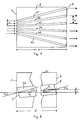
- the arrangement for fanning out In order to achieve a parallel offset between the functional units and thus between the light bundles on the input and output sides, the arrangement for fanning out must provide a double light deflection.
- the light beams in front of and behind the arrangement for fanning out are parallel to one another, the optical waveguide between the light deflections is inclined against the light beams in front of and behind the arrangement by the angle ⁇ i .
- the angle ⁇ i is different for the different light beams. It depends on whether a light beam in an array belongs to the outer or middle light beams. An array is usually constructed symmetrically. For a light beam, the angle ⁇ i results from the parallel offset d i and the overall length l for the arrangement for fanning out.
- ⁇ i arctan (d i / l)
- the normals on the respective end faces of the optical waveguides of the arrangement are inclined at an angle ⁇ i against the light bundles in front of and behind the arrangement. It is thereby achieved that the light bundle coupled into the optical waveguide of the arrangement runs after calculation on the end face on the optical waveguide axis and that the light bundle coupled out of the optical waveguide of the arrangement runs again after refraction in parallel to the other light bundles.
- the normals of the end faces are inclined to the axis of the respective optical waveguide of the arrangement by the angle ⁇ i .
- ⁇ i ⁇ i + ⁇ i
- sin ⁇ i n ⁇ sin ⁇ i
- n is the refractive index of the optical fiber.
- ⁇ i arcsin (n ⁇ sin ⁇ i / (1 - n ⁇ cos ⁇ i ) 2 + n2 ⁇ sin2 ⁇ i ) 1/2 ) Since the parallel offset d i is different for each light beam, the inclination of the end faces is also different for each optical fiber.
- mounting grooves for fiber arrays or microlens arrays to be coupled can be produced by anisotropic etching.
- waveguides made of SiO2 with TiO2 doping can be produced to raise the refractive index in the core area.
- the structuring of the side and end faces of the rib waveguide can be carried out by reactive ion etching using a photoresist mask.
- the high precision required for the coupling is achieved by photolithography, so that adjustment is no longer necessary.
- a functional unit can be, for example, a directional coupler in which the distance between the second light bundles is a few micrometers, a boostructure in which the light bundles are arranged directly next to one another, or a laser or receiving diode line with a spacing of the light bundles of a few tens of micrometers.
- a fiber array, in which the light beam spacing is at least 125 micrometers, or a line with micro-optical imaging components such as spherical lenses, Selfoc lenses or holograms, can also represent a functional unit. In the case of a line with micro-optical imaging components, their mutual distances are at least as large as the diameter of the individual components. These are approximately 1 mm.
- the arrangement for fanning out parallel light bundles into parallel light bundles can be operated with a changed distance in both directions, ie the light can be coupled in both on the side on which the Beams are further apart and are coupled on the side on which the light beams are close to each other.
- the arrangement shown in FIG. 1 for fanning out light beams is structured as follows: On a base plate 3 there are six rectilinear strip waveguides 41 to 46. On the input side, six light beams with the mutual distance a 1 enter the arrangement. The input side of the base plate 3 is referred to as the input face 1. On the exit face 2, the six light beams emerge from the arrangement for fanning out at a distance a2. The optical axes of the incoming and outgoing light beams run parallel to one another and perpendicular to the entrance or exit face 1, 2 of the base plate 3.
- the strip waveguides 41-46 are at the respective angles ⁇ i to the normal on the entrance and exit face 1, 2 inclined. The angular relationships can be seen from the detailed drawing in FIG.
- the strip waveguide 42 has two end faces 5 and 5 'which are at an angle ⁇ i to the axis of the strip waveguide and to the normal on the input or.
- Output side 1, 2 is inclined by the angle ⁇ i .
- the angle of inclination ⁇ i results from the refractive index, so that the light beam on the input side after the refraction at the end face 5 runs exactly in the direction of the axis of the strip waveguide.
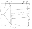
- FIG. 3 shows a top view of a silicon carrier 10 with an anisotropically etched V-groove 11 for receiving an optical fiber 15 or a round optic.
- the silicon carrier carries a buffer layer on which a core layer 13 has been applied and structured. This is surrounded by a cladding layer 14.
- the core layer has a higher refractive index than the buffer layer and the cladding layer.
- the waveguide consisting of core layer 13 and cladding layer 14 is structured on its end face 16 by reactive ion etching. The beveling with the angle ⁇ has not been carried out over the entire waveguide width, but only in the core area and on one side of the core. The distance between the waveguide and the optical fiber 15 can thereby be reduced.
Landscapes
- Physics & Mathematics (AREA)
- General Physics & Mathematics (AREA)
- Optics & Photonics (AREA)
- Engineering & Computer Science (AREA)
- Microelectronics & Electronic Packaging (AREA)
- Optical Couplings Of Light Guides (AREA)
- Optical Integrated Circuits (AREA)
Applications Claiming Priority (2)
| Application Number | Priority Date | Filing Date | Title |
|---|---|---|---|
| DE19904009323 DE4009323C1 (enExample) | 1990-03-23 | 1990-03-23 | |
| DE4009323 | 1990-03-23 |
Publications (2)
| Publication Number | Publication Date |
|---|---|
| EP0447639A1 EP0447639A1 (de) | 1991-09-25 |
| EP0447639B1 true EP0447639B1 (de) | 1994-05-04 |
Family
ID=6402877
Family Applications (1)
| Application Number | Title | Priority Date | Filing Date |
|---|---|---|---|
| EP19900124042 Expired - Lifetime EP0447639B1 (de) | 1990-03-23 | 1990-12-13 | Anordnung zur Auffächerung von Lichtpfaden |
Country Status (2)
| Country | Link |
|---|---|
| EP (1) | EP0447639B1 (enExample) |
| DE (1) | DE4009323C1 (enExample) |
Cited By (1)
| Publication number | Priority date | Publication date | Assignee | Title |
|---|---|---|---|---|
| US6049641A (en) * | 1998-02-24 | 2000-04-11 | Gemfire Corporation | Connection system for optical redundancy |
Families Citing this family (4)
| Publication number | Priority date | Publication date | Assignee | Title |
|---|---|---|---|---|
| WO1993013468A1 (de) * | 1991-12-21 | 1993-07-08 | Richard Hirschmann Gmbh & Co. | Einrichtung zum überwachen eines verschlusses |
| DE19742895C2 (de) * | 1997-09-24 | 1999-10-21 | Siemens Ag | Elektrooptische Anordnung |
| CN110426787B (zh) * | 2019-07-04 | 2020-12-22 | 苏州安捷讯光电科技股份有限公司 | 一种带衰减非接触式光纤回路器及其制作方法 |
| CN118311710B (zh) * | 2024-04-30 | 2025-04-08 | 中国电子科技集团有限公司电子科学研究院 | 一种扇形光纤波导阵列模块 |
Family Cites Families (5)
| Publication number | Priority date | Publication date | Assignee | Title |
|---|---|---|---|---|
| US4094579A (en) * | 1976-09-13 | 1978-06-13 | Sperry Rand Corporation | Multimode optical waveguide device with non-normal butt coupling of fiber to electro-optic planar waveguide |
| JPS57142603A (en) * | 1981-02-27 | 1982-09-03 | Canon Inc | Optical scanner |
| FR2547071B1 (fr) * | 1983-05-31 | 1986-02-14 | Cit Alcatel | Dispositif opto-electronique de commutation spatiale |
| DD279751A1 (de) * | 1986-07-31 | 1990-06-13 | Univ Schiller Jena | Verfahren zur herstellung eines wellenleiterkopplers |
| US4878724A (en) * | 1987-07-30 | 1989-11-07 | Trw Inc. | Electrooptically tunable phase-locked laser array |
-
1990
- 1990-03-23 DE DE19904009323 patent/DE4009323C1/de not_active Expired - Lifetime
- 1990-12-13 EP EP19900124042 patent/EP0447639B1/de not_active Expired - Lifetime
Cited By (1)
| Publication number | Priority date | Publication date | Assignee | Title |
|---|---|---|---|---|
| US6049641A (en) * | 1998-02-24 | 2000-04-11 | Gemfire Corporation | Connection system for optical redundancy |
Also Published As
| Publication number | Publication date |
|---|---|
| DE4009323C1 (enExample) | 1991-02-21 |
| EP0447639A1 (de) | 1991-09-25 |
Similar Documents
| Publication | Publication Date | Title |
|---|---|---|
| DE69522051T2 (de) | Anamorphotische Microlinse zum Einkoppeln elliptischer Lichtstrahlen in optische Fasern | |
| DE69618087T2 (de) | Mechanischer faseroptischer Schalter | |
| DE68924029T2 (de) | Vorrichtung zur optischen Verbindung einer Monomodenfaser mit einer Multimodenfaser. | |
| DE3751674T2 (de) | Optischer Faserkoppler | |
| DE2745940A1 (de) | Optisches schaltkreiselement | |
| DE2614051C2 (de) | Faseroptischer T-Koppler | |
| DE60214186T2 (de) | Verfahren zur Herstellung von optischen Faserkollimatoren im Array | |
| DE69527386T2 (de) | Mit Linse versehener Niveaufühler unter Verwendung eines optischen Punkts | |
| DE3886935T2 (de) | Optisches koppelelement. | |
| DE2436908B2 (de) | Vorrichtung zur Bündelung von Laserstrahlen | |
| DE3854441T2 (de) | Faseroptischer Abzweiger unter Verwendung eines Reflektors. | |
| DE2428570C2 (de) | Anordnung zur optischen Signalübertragung | |
| DE19510559C1 (de) | Optische Sende- und Empfangsanordnung | |
| DE69901650T2 (de) | Optischer Mehrfachkoppler mit Linse | |
| EP0923749B1 (de) | Lichtübertragungsvorrichtung | |
| DE2905916A1 (de) | Faseroptische uebertragungsvorrichtung | |
| US4247165A (en) | Fiber optic plate | |
| EP0447639B1 (de) | Anordnung zur Auffächerung von Lichtpfaden | |
| DE60300998T2 (de) | Optische Vorrichtung zur Sammlung von Laserbündeln und Lichtquellenvorrichtung | |
| DE4214791C1 (enExample) | ||
| EP0667545B1 (de) | Anordnung zur Anpassung unterschiedlicher Feldverteilungen von Lichtstrahlen | |
| DE3788664T2 (de) | Optische Leiter. | |
| EP0453655B1 (de) | Lichtmischer | |
| DE2951020C2 (enExample) | ||
| DE69523006T2 (de) | Faseroptisches Stecker |
Legal Events
| Date | Code | Title | Description |
|---|---|---|---|
| PUAI | Public reference made under article 153(3) epc to a published international application that has entered the european phase |
Free format text: ORIGINAL CODE: 0009012 |
|
| 17P | Request for examination filed |
Effective date: 19901228 |
|
| AK | Designated contracting states |
Kind code of ref document: A1 Designated state(s): FR GB IT NL SE |
|
| 17Q | First examination report despatched |
Effective date: 19930304 |
|
| GRAA | (expected) grant |
Free format text: ORIGINAL CODE: 0009210 |
|
| ITF | It: translation for a ep patent filed | ||
| AK | Designated contracting states |
Kind code of ref document: B1 Designated state(s): FR GB IT NL SE |
|
| ET | Fr: translation filed | ||
| GBT | Gb: translation of ep patent filed (gb section 77(6)(a)/1977) |
Effective date: 19940811 |
|
| EAL | Se: european patent in force in sweden |
Ref document number: 90124042.4 |
|
| PLBE | No opposition filed within time limit |
Free format text: ORIGINAL CODE: 0009261 |
|
| STAA | Information on the status of an ep patent application or granted ep patent |
Free format text: STATUS: NO OPPOSITION FILED WITHIN TIME LIMIT |
|
| 26N | No opposition filed | ||
| PGFP | Annual fee paid to national office [announced via postgrant information from national office to epo] |
Ref country code: NL Payment date: 19961223 Year of fee payment: 7 |
|
| PGFP | Annual fee paid to national office [announced via postgrant information from national office to epo] |
Ref country code: GB Payment date: 19971127 Year of fee payment: 8 |
|
| PGFP | Annual fee paid to national office [announced via postgrant information from national office to epo] |
Ref country code: FR Payment date: 19971218 Year of fee payment: 8 |
|
| PGFP | Annual fee paid to national office [announced via postgrant information from national office to epo] |
Ref country code: SE Payment date: 19971219 Year of fee payment: 8 |
|
| PG25 | Lapsed in a contracting state [announced via postgrant information from national office to epo] |
Ref country code: NL Free format text: LAPSE BECAUSE OF NON-PAYMENT OF DUE FEES Effective date: 19980701 |
|
| NLV4 | Nl: lapsed or anulled due to non-payment of the annual fee |
Effective date: 19980701 |
|
| PG25 | Lapsed in a contracting state [announced via postgrant information from national office to epo] |
Ref country code: GB Free format text: LAPSE BECAUSE OF NON-PAYMENT OF DUE FEES Effective date: 19981213 |
|
| PG25 | Lapsed in a contracting state [announced via postgrant information from national office to epo] |
Ref country code: SE Free format text: LAPSE BECAUSE OF NON-PAYMENT OF DUE FEES Effective date: 19981214 |
|
| GBPC | Gb: european patent ceased through non-payment of renewal fee |
Effective date: 19981213 |
|
| PG25 | Lapsed in a contracting state [announced via postgrant information from national office to epo] |
Ref country code: FR Free format text: LAPSE BECAUSE OF NON-PAYMENT OF DUE FEES Effective date: 19990831 |
|
| REG | Reference to a national code |
Ref country code: FR Ref legal event code: ST |
|
| PG25 | Lapsed in a contracting state [announced via postgrant information from national office to epo] |
Ref country code: IT Free format text: LAPSE BECAUSE OF NON-PAYMENT OF DUE FEES;WARNING: LAPSES OF ITALIAN PATENTS WITH EFFECTIVE DATE BEFORE 2007 MAY HAVE OCCURRED AT ANY TIME BEFORE 2007. THE CORRECT EFFECTIVE DATE MAY BE DIFFERENT FROM THE ONE RECORDED. Effective date: 20051213 |