EP0446908B1 - Commutateur à coordonnées opto-électronique à vitesse élevée - Google Patents
Commutateur à coordonnées opto-électronique à vitesse élevée Download PDFInfo
- Publication number
- EP0446908B1 EP0446908B1 EP91103876A EP91103876A EP0446908B1 EP 0446908 B1 EP0446908 B1 EP 0446908B1 EP 91103876 A EP91103876 A EP 91103876A EP 91103876 A EP91103876 A EP 91103876A EP 0446908 B1 EP0446908 B1 EP 0446908B1
- Authority
- EP
- European Patent Office
- Prior art keywords
- photodetector
- switch
- input
- laser diode
- optical
- Prior art date
- Legal status (The legal status is an assumption and is not a legal conclusion. Google has not performed a legal analysis and makes no representation as to the accuracy of the status listed.)
- Expired - Lifetime
Links
- 230000005693 optoelectronics Effects 0.000 title claims description 8
- 230000003287 optical effect Effects 0.000 claims description 48
- 230000004044 response Effects 0.000 claims description 15
- 230000009849 deactivation Effects 0.000 claims description 12
- 238000000034 method Methods 0.000 claims description 6
- 238000005286 illumination Methods 0.000 claims description 5
- 239000013307 optical fiber Substances 0.000 description 7
- 229910000530 Gallium indium arsenide Inorganic materials 0.000 description 3
- 239000003990 capacitor Substances 0.000 description 3
- 238000004891 communication Methods 0.000 description 3
- 230000003247 decreasing effect Effects 0.000 description 3
- 239000000835 fiber Substances 0.000 description 3
- 230000001965 increasing effect Effects 0.000 description 3
- 238000010586 diagram Methods 0.000 description 2
- 238000002955 isolation Methods 0.000 description 2
- 230000015654 memory Effects 0.000 description 2
- 238000012986 modification Methods 0.000 description 2
- 230000004048 modification Effects 0.000 description 2
- 238000012545 processing Methods 0.000 description 2
- 238000012546 transfer Methods 0.000 description 2
- 230000004913 activation Effects 0.000 description 1
- 230000005540 biological transmission Effects 0.000 description 1
- 230000008859 change Effects 0.000 description 1
- 230000008878 coupling Effects 0.000 description 1
- 238000010168 coupling process Methods 0.000 description 1
- 238000005859 coupling reaction Methods 0.000 description 1
- 238000011161 development Methods 0.000 description 1
- 230000000694 effects Effects 0.000 description 1
- 230000001939 inductive effect Effects 0.000 description 1
- 238000007689 inspection Methods 0.000 description 1
- 230000003993 interaction Effects 0.000 description 1
- 239000002184 metal Substances 0.000 description 1
- 230000003071 parasitic effect Effects 0.000 description 1
- 230000009467 reduction Effects 0.000 description 1
- 230000007704 transition Effects 0.000 description 1
Images
Classifications
-
- H—ELECTRICITY
- H03—ELECTRONIC CIRCUITRY
- H03K—PULSE TECHNIQUE
- H03K17/00—Electronic switching or gating, i.e. not by contact-making and –breaking
- H03K17/51—Electronic switching or gating, i.e. not by contact-making and –breaking characterised by the components used
- H03K17/56—Electronic switching or gating, i.e. not by contact-making and –breaking characterised by the components used by the use, as active elements, of semiconductor devices
- H03K17/687—Electronic switching or gating, i.e. not by contact-making and –breaking characterised by the components used by the use, as active elements, of semiconductor devices the devices being field-effect transistors
- H03K17/693—Switching arrangements with several input- or output-terminals, e.g. multiplexers, distributors
-
- H—ELECTRICITY
- H03—ELECTRONIC CIRCUITRY
- H03K—PULSE TECHNIQUE
- H03K17/00—Electronic switching or gating, i.e. not by contact-making and –breaking
- H03K17/51—Electronic switching or gating, i.e. not by contact-making and –breaking characterised by the components used
- H03K17/78—Electronic switching or gating, i.e. not by contact-making and –breaking characterised by the components used using opto-electronic devices, i.e. light-emitting and photoelectric devices electrically- or optically-coupled
Definitions
- the present invention relates to a high speed opto-electronic crossbar switch for selectively connecting signals carried by first and second input optimal beams to an output node, said crossbar switch comprising:
- the present invention further relates to a method for selectively connecting signals carried by first and second input optical beams to an output node, comprising the steps of:
- a crossbar switch and a respective method are disclosed in document DE-OS-2 424 899.
- optical signals each travelling along an optical fiber are selectively coupled to an amplifier by applying respective control voltages to an optical crossbar switch.
- the optical fibers are aligned with photodiodes arranged in parallel, the output node of said parallel arrangement being connected to the amplifier.
- Each photodiode has arranged in series a transistor switch which is under the control of control voltages. Depending on the state of the single transistor switches the photodiodes are switched through to the amplifier.
- the present invention relates in general to signal switching devices. More specifically, the present invention relates to apparatus for switching a plurality of signals in communication networks.
- Parallel processors commonly include a large number of processors that execute programs concurrently or in parallel. These architectures typically require a communication network that allows efficient data transfer between processors, and between an individual processor and its associated memories. In many parallel processing systems it is desirable to permit many processors to transfer information simultaneously. Employing optics in parallel processing is particularly effective given the relatively large bandwidth attainable, and the typically low interaction among individual optical beams in linear media.
- One optical system used in this context is known as a crossbar network.
- a crossbar network permits a plurality of processors or memories to be dynamically interconnected in a selected configuration without mechanically moving existing interconnections.
- Certain crossbar networks are realized completely electronically. That is, resort is not made to the optical domain until a selected number of input data channels have been placed in electrical communication with a desired array of output channels. Only then is data present on the electrical output channels used to modulate an optical carrier, which is subsequently transmitted to a selected destination. Unfortunately, this mode of electronic switching is relatively slow and may impede the overall speed of the computing network in which it is utilized.
- crossbar networks are operative entirely in the optical domain.
- a selected number of optical input beams are interconnected via optical elements to a chosen set of optical output channels, as disclosed in DE-OS-2 424 899, mentioned at the outset.
- channel switching effected entirely in the optical domain is slow, as is channel switching entirely in the electronic domain.
- conventional exclusively optical switching networks are marked by poor interchannel isolation. That is, adjacent optical channels are prone to substantial mutual interference which may degrade overall system performance.
- the new crossbar switch is disposed to obviate the need for high input optical signal power.
- Optical energy from the laser diode means which irradiates the selected photodetector induces a photo-generated current to flow therein. This photo-generated current, aids in dissipating the residual voltage present on the selected photodetector due to the intrinsic capacitance, thus increasing the photodetector deactivation rate and, further, the switching rate of the new crossbar switch.
- the need in the art identified above is addressed by the high speed opto-electronic crossbar switch of the present invention.
- the inventive crossbar switch is disposed to selectively connect signals carried by first and second input optical beams to an output node.
- the switch of the present invention includes a selectively actuatable photodetector network for converting the signals carried by the first and second input beams to electrical output signals, and for impressing these output signals upon the output node.
- the photodetector network has a first photodetector in optical alignment with the first input beam, and a second photodetector in optical alignment with the second input beam.
- the inventive crossbar switch further includes a multiplexer for actuating the first and second photodetectors in response to a control signal.
- the present invention also includes a laser diode circuit for illuminating the first and second photodetectors in response to the control signal.
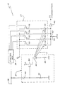
- the Figure is a block diagram representing the high speed opto-electronic crossbar switch of the present invention.
- the Figure is a block diagram representing the high speed opto-electronic crossbar switch 10 of the present invention.
- the opto-electronic switch 10 includes a photodetector network 22, a laser diode circuit 24 and a control multiplexer 26.
- the photodetector network 22 includes, in this particular embodiment, four separate photodetectors 30, 32, 34, 36. A number other than four works just as well, depending on the application.
- Each photodetector 30-36 is individually coupled to an optical fiber (not shown for clarity), with each fiber carrying an input optical data beam. The data beam illuminates the photodetector 30-36 coupled thereto.
- a control signal impressed upon an input node 38 directs the control multiplexer 26 to actuate one or more of the photodetectors 30-36, which then each generate photocurrent in response to the optical data beam impinging thereon. Flow of this photocurrent through a resistor 40 induces an output signal voltage to be impressed upon an output node 42. An amplifier 46 coupled to the output node 42 amplifies the input signal voltage for transmission. In this manner signals carried by four optical data beams may be selectively switched to a single output channel.
- one change of state of the switch 10 is effected by impressing a control signal upon the input node 38, thereby inducing one or more of the photodetectors 30-36 to be deactivated.
- Application of this control signal also causes a laser diode 44 within the diode circuit 24 to briefly flash. This flash illuminates the photodetectors 30-36 with optical energy E immediately subsequent to the deactivation of one or more thereof.
- the one or more photodetectors 30-36 selected for deactivation then generate photocurrent in response to the illuminative pulse emitted by the diode 44. This photocurrent aids in dissipating the residual voltage (due to intrinsic capacitance) across each photodetector 30-36 selected for deactivation.
- Accelerated dissipation of this residual voltage expedites transition of a selected photodetector 30-36 to the deactivated state, thereby decreasing the deactivation time thereof.
- the corresponding reduction in the switching time of the crossbar switch 10 due to this decrease in photodetector deactivation time is a feature of the present invention.
- the photodetector network 22 includes four photodetectors 30, 32, 34, 36. Again, each of the photodetectors 30-36 is conventionally coupled to an optical fiber associated with an optical channel. Alternatively, the input optical fibers may be terminated with optical lenses which transmit the optical beams carried thereby to the appropriate photodetector 30-36. In this latter configuration the optical fibers do not physically contact the photodetectors 30-36.
- each photodetector 30-36 is an InGaAs p-i-n diode. The use of p-i-n diodes is preferred as a result of their fast switching capability.
- CMOS devices for the multiplexer 26 are generally preferred due to their large input impedance when in the nonconducting state.
- the multiplexer 26 is operative to selectively couple a suitable bias source V B to a photodetector 30-36 by turning on an appropriate MOSFET device 50, 52, 54, 56.
- a photodetector 30-36 can be switched to the "on” state by applying an appropriate control signal to the multiplexer 26 via the input node 38.
- the control signal is decoded by the multiplexer 26 to provide a suitably actuating gate voltage on one of the MOSFET devices 50-56, thereby coupling the bias voltage V B to the selected photodetector 30-36.
- Each photodetector 30-36 has associated parasitic capacitances C p (V) and C s , where V is the voltage across the photodetector.
- the voltage remaining on the photodetector 30-36 (due to C p (V) and C s ) subsequent to opening the switch 50-56 may then only be dissipated by current I o generated by the photodetector 30-36.
- the photo-generated current I o is produced in response to illumination of the photodetector 30-36 by the optical data beam incident thereon.
- the input signal power incident on the photodetectors of conventional crossbar switches is required to be approximately 1 mW. This requirement is too high for many applications, and limits optical fanout (the number of data channels into which an input optical carrier may be subdivided).
- the switch 10 of the present invention is disposed to obviate the need for high input optical signal power by utilizing the laser diode 44 to supply additional optical power to the photodetectors 30-36.
- a control signal is applied to the input node 38.
- the control signal is decoded by the control multiplexer 26, which then impresses a gate voltage of a first polarity on the MOSFET 50-56 coupled to the selected photodetector 30-36.
- the gate voltage applied to the MOSFET 50-56 decouples the selected photodetector 30-36 from the voltage source V B , thereby interrupting external current flow to the selected photodetector 30-36.
- a V B of approximately -2 volts may be employed without a sacrifice in detector bandwidth.
- control signal to the input node 38 also induces a voltage to develop across a capacitor 60.
- the accompanying current flow through a resistor 62 causes a voltage of a second polarity, opposite to that of the first polarity, to impinge on the gate of a MOSFET 64.
- the multiplexer 26 may be designed to deliver a gate voltage of the first polarity to the selected MOSFET 50- 56 when a control signal is applied at node 38 that causes development of a gate voltage of the second polarity at MOSFET 64.
- the values of the capacitor 60 and resistor 62 may be chosen such that the voltage at the gate of the MOSFET 64 reaches the "turn-on" voltage thereof substantially contemporaneously with decoupling of the selected photodetector 30-36 from the source V B .
- the laser diode 44 is connected to a voltage source V LD at approximately the time at which the externally supplied current to the selected photodetector 30-36 is interrupted. Connection of the laser diode 44 to the source V LD induces current flow through the laser diode 44 and resistor 45, and causes the laser diode 44 to illuminate the selected photodetector 30-36 for as long as the turn-on voltage at the gate of the MOSFET 64 is maintained.
- Optical energy from the laser diode 44 which irradiates the selected photodetector 30-36 induces a photogenerated current to flow therein. Again, this photogenerated current expedites the subsidence of residual voltage present on the selected photodetector 30-36 due to the intrinsic capacitance C p (V) and C s thereof.
- the relative values of the capacitor 60 and resistor 62 may be adjusted such that the requisite voltage to activate the MOSFET 64 subsists at the gate thereof for the desired illumination interval.
- different circuits are possible within the scope of the present invention.
- the selected photodetector 30-36 may need to be illuminated by the laser diode 44 over an interval of approximately 1 ns to effect a 10 ns switching rate. This switching speed appears to be between two and three orders of magnitude faster than that exhibited by conventional crossbar switching schemes.
- the present invention is not limited to the RC laser diode timing circuit disclosed herein. Those of ordinary skill in the art may be aware of other networks for maintaining the requisite turn-on voltage at the gate of the MOSFET 64.
Landscapes
- Electronic Switches (AREA)
- Multi Processors (AREA)
- Use Of Switch Circuits For Exchanges And Methods Of Control Of Multiplex Exchanges (AREA)
- Optical Communication System (AREA)
Claims (10)
- Commutateur crossbar optoélectronique à grande vitesse pour le transfert sélectif de signaux véhiculés par des premier et second faisceaux optiques d'entrée à un noeud de sortie (42), ledit commutateur crossbar (10) comprenant :- des moyens photodétecteurs (22), pouvant être actionnés de façon sélective, comprenant un premier photodétecteur (30) aligné optiquement avec ledit premier faisceau d'entrée et un second photodétecteur (32) aligné optiquement avec ledit second faisceau d'entrée, pour convertir lesdits signaux véhiculés par lesdits premier et second faisceaux d'entrée en des signaux de sortie électriques, lesdits moyens formant photodétecteurs (22) comprenant des moyens pour appliquer lesdits signaux de sortie audit noeud de sortie (42); et- des moyens formant multiplexeur (26) pour désactiver au moins l'un desdits premier et second photodétecteurs (30, 32) en réponse à un signal de commande; caractérisé par :- des moyens à diode laser (24) pour éclairer brièvement le photodétecteur (30,32) désactivé par lesdits moyens formant multiplexeur (26) en réponse audit signal de commande pour réduire la durée de désactivation.
- Commutateur selon la revendication 1, caractérisé en ce que lesdits moyens formant photodétecteurs (22), pouvant être actionnés de façon sélective, comprennent des premier et second photodétecteurs (30,32) respectivement alignés optiquement avec lesdits premier et second faisceaux de signaux optiques, lesdits photodétecteurs (30,32) produisant un courant proportionnel auxdits signaux de sortie lors de l'éclairement par lesdits faisceaux de signaux optiques.
- Commutateur selon la revendication 1 ou 2, caractérisé en ce que ledit premier photodétecteur (30) est branché en série entre ledit noeud de sortie (42) et un premier interrupteur à transistor (50), et ledit second photodétecteur (32) est branché en série entre ledit noeud de sortie (42) et un second interrupteur à transistor (52), lesdits premier et second interrupteurs à transistors (50, 52) possédant chacun une borne de commande couplée électriquement auxdits moyens formant multiplexeur (26).
- Commutateur selon la revendication 3, caractérisé en ce que lesdits premier et second interrupteurs à transistors (50,52) sont en outre couplés chacun à une source de polarisation (VB) .
- Commutateur selon l'une quelconque des revendications 1 à 4, caractérisé en ce que lesdits moyens à diode laser (24) et lesdits moyens formant multiplexeur (26) sont couplés électriquement à un noeud d'entrée (38), et comportent en outre des moyens pour appliquer ledit signal de commande audit noeud d'entrée (38).
- Commutateur selon l'une quelconque des revendications 1 à 5, caractérisé en ce que lesdits moyens à diode laser (24) comprennent :- une diode laser (44);- un réseau de cadencement (60,62) couplé audit noeud d'entrée (38) ; et- un interrupteur à transistor (64) branché en série entre ladite diode laser (44) et ledit réseau de cadencement (60,62) .
- Commutateur selon l'une quelconque des revendications 1 à 6, caractérisé en ce que lesdits moyens d'application desdits signaux de sortie incluent un réseau résistif (40) couplé audit noeud de sortie (42) pour convertir lesdits courants de signal desdits premier et second photodétecteurs (30,32) en des tensions de signal appliquées audit noeud de sortie (40).
- Commutateur selon l'une quelconque des revendications 1 à 7, caractérisé par un amplificateur de tension (46) couplé audit noeud de sortie (42).
- Commutateur selon la revendication 1, caractérisé en ce que lesdits moyens à diode laser (24) comprennent :- une diode laser (44);- un interrupteur électronique (64) couplé à ladite diode laser (44); et- un réseau de cadencement (60,62) couplé audit interrupteur électronique (64) pour retransmettre à ce dernier ledit signal de commande.
- Procédé pour transférer de façon sélective des signaux véhiculés par des premier et second faisceaux optiques d'entrée à un noeud de sortie (42), comprenant les étapes consistant à :a) positionner un premier photodétecteur (30) d'une manière alignée optiquement avec ledit premier faisceau d'entrée, et un second photodétecteur (32) d'une manière alignée optiquement avec ledit second faisceau d'entrée;b) convertir lesdits signaux véhiculés par lesdits premier et second faisceaux d'entrée en des signaux de sortie électriques;c) appliquer lesdits signaux de sortie audit noeud de sortie (42); etd) désactiver au moins l'un desdits premier et second photodétecteurs (30,32) en réponse à un signal de commande;caractérisé par l'étape supplémentaire consistant à :
e) éclairer brièvement ledit photodétecteur désactivé (30,32) en réponse audit signal de commande pour réduire la durée de désactivation.
Applications Claiming Priority (2)
| Application Number | Priority Date | Filing Date | Title |
|---|---|---|---|
| US07/494,640 US5072439A (en) | 1990-03-16 | 1990-03-16 | High speed opto-electronic crossbar switch |
| US494640 | 1990-03-16 |
Publications (3)
| Publication Number | Publication Date |
|---|---|
| EP0446908A2 EP0446908A2 (fr) | 1991-09-18 |
| EP0446908A3 EP0446908A3 (en) | 1991-11-27 |
| EP0446908B1 true EP0446908B1 (fr) | 1996-09-18 |
Family
ID=23965332
Family Applications (1)
| Application Number | Title | Priority Date | Filing Date |
|---|---|---|---|
| EP91103876A Expired - Lifetime EP0446908B1 (fr) | 1990-03-16 | 1991-03-14 | Commutateur à coordonnées opto-électronique à vitesse élevée |
Country Status (4)
| Country | Link |
|---|---|
| US (1) | US5072439A (fr) |
| EP (1) | EP0446908B1 (fr) |
| JP (1) | JPH04227395A (fr) |
| DE (1) | DE69122145T2 (fr) |
Families Citing this family (7)
| Publication number | Priority date | Publication date | Assignee | Title |
|---|---|---|---|---|
| JPH04280522A (ja) * | 1991-03-08 | 1992-10-06 | Nec Corp | 光接続装置とその駆動方法 |
| JPH0561432A (ja) * | 1991-08-29 | 1993-03-12 | Sharp Corp | 液晶ドライバ回路 |
| AT992U1 (de) * | 1994-01-20 | 1996-08-26 | Lang Alois Ing | Optoelektronisches system zur auslösung von signalen |
| US7466914B2 (en) * | 2005-01-21 | 2008-12-16 | The Board Of Trustees Of The Leland Stanford Junior University | Optoelectronic switch having cascaded optical nodes |
| JP2007110285A (ja) * | 2005-10-12 | 2007-04-26 | Dx Antenna Co Ltd | 光−電気変換出力装置 |
| US8312193B2 (en) * | 2010-01-08 | 2012-11-13 | International Business Machines Corporation | Eager protocol on a cache pipeline dataflow |
| US20140314406A1 (en) * | 2011-12-09 | 2014-10-23 | Rambus Inc. | Systems and Methods for Temperature Insensitive Photonic Transmission |
Family Cites Families (22)
| Publication number | Priority date | Publication date | Assignee | Title |
|---|---|---|---|---|
| JPS5071377A (fr) * | 1973-05-22 | 1975-06-13 | ||
| US3883222A (en) * | 1973-09-07 | 1975-05-13 | Corning Glass Works | Coupler for optical communication system |
| DE2415046A1 (de) * | 1974-03-28 | 1975-10-02 | Siemens Ag | Vorrichtung zur verteilung von lichtsignalen auf mehrere empfaenger |
| US4165225A (en) * | 1975-04-17 | 1979-08-21 | Siemens Aktiengesellschaft | Distributor for optical signals |
| US4074142A (en) * | 1975-09-10 | 1978-02-14 | Jackson Albert S | Optical cross-point switch |
| US4221932A (en) * | 1978-11-02 | 1980-09-09 | Bell Telephone Laboratories, Incorporated | Infrared remote signaling system |
| DE2916184A1 (de) * | 1979-04-21 | 1980-10-30 | Philips Patentverwaltung | Optischer leistungsteiler |
| US4369371A (en) * | 1980-11-24 | 1983-01-18 | Canadian Patents & Dev. Limited | Broadband high speed optoelectronic semiconductor switch |
| FR2520960B1 (fr) * | 1982-02-03 | 1986-12-12 | Rozenwaig Boris | Perfectionnements aux commutateurs opto-electriques a recepteurs multicellules |
| DE3213839A1 (de) * | 1982-04-15 | 1983-10-27 | Philips Patentverwaltung Gmbh, 2000 Hamburg | Optische wellenlaengen-multiplex- bzw. -demultiplexanordnung |
| CA1225121A (fr) * | 1982-11-05 | 1987-08-04 | Motomu Mochizuki | Reseau optique a architecture de bus pouvant detecter rapidement les collisions a chaque station de communication |
| JPS6021706U (ja) * | 1983-07-19 | 1985-02-14 | アルプス電気株式会社 | スタ−カプラ |
| US4696059A (en) * | 1984-03-07 | 1987-09-22 | Canadian Patents And Development Limited-Societe Canadienne Des Brevets Et D'exploitation Limitee | Reflex optoelectronic switching matrix |
| US4783850A (en) * | 1984-03-07 | 1988-11-08 | Canadian Patents And Development Limited-Societe Canadienne Des Brevets Et D'exploitation Limitee | Optoelectronic compound switching matrix |
| EP0161683B1 (fr) * | 1984-05-17 | 1993-08-11 | Nec Corporation | Circuit commutateur optique |
| FR2566220B1 (fr) * | 1984-06-15 | 1986-08-22 | Cit Alcatel | Selecteur opto-electronique |
| US4630254A (en) * | 1984-10-26 | 1986-12-16 | Trw Inc. | Controlled star network |
| JPS61184997A (ja) * | 1985-02-12 | 1986-08-18 | Nec Corp | 光時間スイツチ |
| EP0216167A3 (fr) * | 1985-09-25 | 1988-10-05 | Siemens Aktiengesellschaft | Réseau d'extension pour augmenter le nombre de raccordements d'abonnés à un système de bus passif optique avec des mélangeurs optiques |
| US4811210A (en) * | 1985-11-27 | 1989-03-07 | Texas Instruments Incorporated | A plurality of optical crossbar switches and exchange switches for parallel processor computer |
| US4901305A (en) * | 1987-12-28 | 1990-02-13 | Tangonan Gregory L | Distributed crossbar switch |
| US4953155A (en) * | 1988-01-20 | 1990-08-28 | Hughes Aircraft Company | Current summed optoelectronic crossbar switch |
-
1990
- 1990-03-16 US US07/494,640 patent/US5072439A/en not_active Expired - Lifetime
-
1991
- 1991-03-14 DE DE69122145T patent/DE69122145T2/de not_active Expired - Fee Related
- 1991-03-14 EP EP91103876A patent/EP0446908B1/fr not_active Expired - Lifetime
- 1991-03-15 JP JP3075660A patent/JPH04227395A/ja active Pending
Also Published As
| Publication number | Publication date |
|---|---|
| DE69122145T2 (de) | 1997-04-10 |
| EP0446908A3 (en) | 1991-11-27 |
| JPH04227395A (ja) | 1992-08-17 |
| EP0446908A2 (fr) | 1991-09-18 |
| US5072439A (en) | 1991-12-10 |
| DE69122145D1 (de) | 1996-10-24 |
Similar Documents
| Publication | Publication Date | Title |
|---|---|---|
| US4959540A (en) | Optical clock system with optical time delay means | |
| US4820914A (en) | Gain control of photomultiplier tubes used in detecting differential absorption lidar returns | |
| US5541756A (en) | Apparatus and method for routing optical signals through wavelength-coding in a self-routed wavelength addressable network | |
| SE462069B (sv) | Signalanordning foer fellokalisering i ett digitaloptiskt oeverfoeringssystem | |
| CA1160697A (fr) | Commutateur optoelectronique a semiconducteur a grande vitesse et a large bande | |
| US4506151A (en) | Optoelectronic logic | |
| EP0446908B1 (fr) | Commutateur à coordonnées opto-électronique à vitesse élevée | |
| JPH02503142A (ja) | 電流合計オプトエレクトロニッククロスバースイッチ | |
| EP0654905B1 (fr) | Récepteur optique à base de transistors à effet de champ | |
| US6563539B1 (en) | Charge transfer circuit for use in imaging systems | |
| ATE176969T1 (de) | Optische nebenschlussvorrichtung | |
| US4286171A (en) | Optoelectric cross-point switch | |
| US5594256A (en) | High voltage switch for pockels cells | |
| US5271074A (en) | Integrated optical waveguide apparatus | |
| EP0224542A1 (fr) | Assemblage et dispositif a logique optique. | |
| US5247183A (en) | Cryogenic signal coupler having imaging lens within a thermal barrier region for optoelectronic coupling | |
| US4744105A (en) | Receiver using optical feedback | |
| CA2134256C (fr) | Dispositif et methode pour etablir un niveau de reference pour un recepteur optique | |
| EP0692873B1 (fr) | Dispositif pour la conversion de signaux optiques bipolaires en signaux unipolaires | |
| CA2074985A1 (fr) | Circuit integre optoelectronique | |
| CA2060689C (fr) | Circuit de commande optique pour circuit integre monolithique hyperfrequence | |
| JP2524464B2 (ja) | 光受信器及び光デ―タリンク | |
| KR890702007A (ko) | 조셉슨 접합을 이용한 광파장 분석기 및 영상처리 시스템 | |
| JP3752620B2 (ja) | 単一光クロックパルス発生方法および回路 | |
| KR900015487A (ko) | 가변성 광 섬유 지연 라인 |
Legal Events
| Date | Code | Title | Description |
|---|---|---|---|
| PUAI | Public reference made under article 153(3) epc to a published international application that has entered the european phase |
Free format text: ORIGINAL CODE: 0009012 |
|
| AK | Designated contracting states |
Kind code of ref document: A2 Designated state(s): DE FR GB |
|
| PUAL | Search report despatched |
Free format text: ORIGINAL CODE: 0009013 |
|
| AK | Designated contracting states |
Kind code of ref document: A3 Designated state(s): DE FR GB |
|
| 17P | Request for examination filed |
Effective date: 19920512 |
|
| 17Q | First examination report despatched |
Effective date: 19950130 |
|
| GRAH | Despatch of communication of intention to grant a patent |
Free format text: ORIGINAL CODE: EPIDOS IGRA |
|
| GRAH | Despatch of communication of intention to grant a patent |
Free format text: ORIGINAL CODE: EPIDOS IGRA |
|
| GRAA | (expected) grant |
Free format text: ORIGINAL CODE: 0009210 |
|
| AK | Designated contracting states |
Kind code of ref document: B1 Designated state(s): DE FR GB |
|
| REF | Corresponds to: |
Ref document number: 69122145 Country of ref document: DE Date of ref document: 19961024 |
|
| ET | Fr: translation filed | ||
| PLBE | No opposition filed within time limit |
Free format text: ORIGINAL CODE: 0009261 |
|
| STAA | Information on the status of an ep patent application or granted ep patent |
Free format text: STATUS: NO OPPOSITION FILED WITHIN TIME LIMIT |
|
| 26N | No opposition filed | ||
| REG | Reference to a national code |
Ref country code: GB Ref legal event code: 732E |
|
| REG | Reference to a national code |
Ref country code: FR Ref legal event code: TP Ref country code: FR Ref legal event code: CD Ref country code: FR Ref legal event code: CA |
|
| REG | Reference to a national code |
Ref country code: GB Ref legal event code: IF02 |
|
| PGFP | Annual fee paid to national office [announced via postgrant information from national office to epo] |
Ref country code: FR Payment date: 20020211 Year of fee payment: 12 |
|
| PGFP | Annual fee paid to national office [announced via postgrant information from national office to epo] |
Ref country code: GB Payment date: 20020220 Year of fee payment: 12 |
|
| PGFP | Annual fee paid to national office [announced via postgrant information from national office to epo] |
Ref country code: DE Payment date: 20020221 Year of fee payment: 12 |
|
| PG25 | Lapsed in a contracting state [announced via postgrant information from national office to epo] |
Ref country code: GB Free format text: LAPSE BECAUSE OF NON-PAYMENT OF DUE FEES Effective date: 20030314 |
|
| PG25 | Lapsed in a contracting state [announced via postgrant information from national office to epo] |
Ref country code: DE Free format text: LAPSE BECAUSE OF NON-PAYMENT OF DUE FEES Effective date: 20031001 |
|
| GBPC | Gb: european patent ceased through non-payment of renewal fee |
Effective date: 20030314 |
|
| PG25 | Lapsed in a contracting state [announced via postgrant information from national office to epo] |
Ref country code: FR Free format text: LAPSE BECAUSE OF NON-PAYMENT OF DUE FEES Effective date: 20031127 |
|
| REG | Reference to a national code |
Ref country code: FR Ref legal event code: ST |