EP0446323B1 - Housing for an electronic circuit - Google Patents
Housing for an electronic circuit Download PDFInfo
- Publication number
- EP0446323B1 EP0446323B1 EP90914067A EP90914067A EP0446323B1 EP 0446323 B1 EP0446323 B1 EP 0446323B1 EP 90914067 A EP90914067 A EP 90914067A EP 90914067 A EP90914067 A EP 90914067A EP 0446323 B1 EP0446323 B1 EP 0446323B1
- Authority
- EP
- European Patent Office
- Prior art keywords
- housing
- circuit board
- frame
- printed circuit
- plastic
- Prior art date
- Legal status (The legal status is an assumption and is not a legal conclusion. Google has not performed a legal analysis and makes no representation as to the accuracy of the status listed.)
- Expired - Lifetime
Links
- 238000002485 combustion reaction Methods 0.000 claims abstract description 4
- 239000002991 molded plastic Substances 0.000 claims abstract description 3
- 239000004033 plastic Substances 0.000 claims description 53
- 239000002184 metal Substances 0.000 claims description 14
- 238000001816 cooling Methods 0.000 claims description 8
- 238000000034 method Methods 0.000 claims description 8
- 238000005476 soldering Methods 0.000 claims description 8
- 238000005452 bending Methods 0.000 claims description 3
- 239000004020 conductor Substances 0.000 claims description 3
- 229910000679 solder Inorganic materials 0.000 claims description 2
- 230000017525 heat dissipation Effects 0.000 abstract description 11
- 238000004519 manufacturing process Methods 0.000 description 6
- 238000003466 welding Methods 0.000 description 4
- 238000010438 heat treatment Methods 0.000 description 3
- 238000001746 injection moulding Methods 0.000 description 3
- 238000001125 extrusion Methods 0.000 description 2
- 238000007789 sealing Methods 0.000 description 2
- 230000035508 accumulation Effects 0.000 description 1
- 238000009825 accumulation Methods 0.000 description 1
- 238000004026 adhesive bonding Methods 0.000 description 1
- 238000010276 construction Methods 0.000 description 1
- 230000007613 environmental effect Effects 0.000 description 1
- 238000005304 joining Methods 0.000 description 1
- 238000001465 metallisation Methods 0.000 description 1
- 230000002093 peripheral effect Effects 0.000 description 1
- 229920000642 polymer Polymers 0.000 description 1
- 239000004065 semiconductor Substances 0.000 description 1
- 239000000243 solution Substances 0.000 description 1
- 239000002470 thermal conductor Substances 0.000 description 1
- 230000007704 transition Effects 0.000 description 1
Images

Classifications
-
- H—ELECTRICITY
- H05—ELECTRIC TECHNIQUES NOT OTHERWISE PROVIDED FOR
- H05K—PRINTED CIRCUITS; CASINGS OR CONSTRUCTIONAL DETAILS OF ELECTRIC APPARATUS; MANUFACTURE OF ASSEMBLAGES OF ELECTRICAL COMPONENTS
- H05K7/00—Constructional details common to different types of electric apparatus
- H05K7/20—Modifications to facilitate cooling, ventilating, or heating
- H05K7/20845—Modifications to facilitate cooling, ventilating, or heating for automotive electronic casings
- H05K7/20854—Heat transfer by conduction from internal heat source to heat radiating structure
-
- B—PERFORMING OPERATIONS; TRANSPORTING
- B29—WORKING OF PLASTICS; WORKING OF SUBSTANCES IN A PLASTIC STATE IN GENERAL
- B29C—SHAPING OR JOINING OF PLASTICS; SHAPING OF MATERIAL IN A PLASTIC STATE, NOT OTHERWISE PROVIDED FOR; AFTER-TREATMENT OF THE SHAPED PRODUCTS, e.g. REPAIRING
- B29C65/00—Joining or sealing of preformed parts, e.g. welding of plastics materials; Apparatus therefor
- B29C65/02—Joining or sealing of preformed parts, e.g. welding of plastics materials; Apparatus therefor by heating, with or without pressure
- B29C65/18—Joining or sealing of preformed parts, e.g. welding of plastics materials; Apparatus therefor by heating, with or without pressure using heated tools
-
- B—PERFORMING OPERATIONS; TRANSPORTING
- B29—WORKING OF PLASTICS; WORKING OF SUBSTANCES IN A PLASTIC STATE IN GENERAL
- B29C—SHAPING OR JOINING OF PLASTICS; SHAPING OF MATERIAL IN A PLASTIC STATE, NOT OTHERWISE PROVIDED FOR; AFTER-TREATMENT OF THE SHAPED PRODUCTS, e.g. REPAIRING
- B29C66/00—General aspects of processes or apparatus for joining preformed parts
- B29C66/50—General aspects of joining tubular articles; General aspects of joining long products, i.e. bars or profiled elements; General aspects of joining single elements to tubular articles, hollow articles or bars; General aspects of joining several hollow-preforms to form hollow or tubular articles
- B29C66/51—Joining tubular articles, profiled elements or bars; Joining single elements to tubular articles, hollow articles or bars; Joining several hollow-preforms to form hollow or tubular articles
- B29C66/54—Joining several hollow-preforms, e.g. half-shells, to form hollow articles, e.g. for making balls, containers; Joining several hollow-preforms, e.g. half-cylinders, to form tubular articles
-
- B—PERFORMING OPERATIONS; TRANSPORTING
- B29—WORKING OF PLASTICS; WORKING OF SUBSTANCES IN A PLASTIC STATE IN GENERAL
- B29L—INDEXING SCHEME ASSOCIATED WITH SUBCLASS B29C, RELATING TO PARTICULAR ARTICLES
- B29L2031/00—Other particular articles
- B29L2031/34—Electrical apparatus, e.g. sparking plugs or parts thereof
- B29L2031/3425—Printed circuits
Definitions
- the invention relates to a housing for an electronic circuit provided with a connector, in particular for control unit electronics of an internal combustion engine of a vehicle, with a frame to which a circuit board having the electronic circuit is fastened, and with a heat sink, the power components of the electronic circuit are assigned, as well as with a cover encompassing the printed circuit board.
- a housing is known from EP-A-0 335 783.
- the subject of the invention with the features mentioned in the main claim has the advantage that with a very simple, inexpensive design, there is a tightly fitting housing that has excellent heat dissipation properties for heat-generating components. It has an injection-molded plastic frame into which at least one heat-conducting web of at least one heat sink is molded. During manufacture, the heat conducting web is embedded in the plastic injection molding process, so that a gap-free and tight design is ensured. One end of the heat conducting web merges into a component mounting surface located inside the housing and the other end of the heat conducting web is designed as a heat dissipation element located outside the housing.
- the heat generated by components arranged on the component mounting surface is therefore directly above the embedded one Thermal conductor led out of the interior of the housing, so that excellent cooling properties are available.
- heat is dissipated through the heat dissipation element, preferably in one piece between the component mounting surface, the heat conducting web and the heat dissipation element, so that extremely small heat transfer resistances are present.
- the plastic frame represents a particularly simple and inexpensive solution.
- the heat sink is preferably made of metal.
- a double function is taken over by the heat dissipation element if it is simultaneously designed as a housing attachment connection.
- the heat dissipation properties are hereby further improved, since the heat transported by the heat conducting web is absorbed or transmitted via the fastening, so that heat accumulations are avoided.
- the housing fastening connection is a flange provided with a bore for a fastening element.
- the heat supplied to the flange can therefore be passed on to a supporting structure or the like via the fastening element.
- the housing accommodates control unit electronics for an internal combustion engine, the heat generated by the corresponding power semiconductors is dissipated to the chassis or body of the motor vehicle via, for example, fastening elements designed as threaded screws. This leads to excellent cooling properties.
- a connector is provided. This can be fixed in a particularly simple manner on the housing when it is molded into the plastic frame.
- the connector is overmolded with plastic during frame production. This guarantees a gap-free transition to the plastic frame even with the connector.
- the plastic frame has molded-on snap projections which can be snapped into holes in the printed circuit board.
- the circuit board can thus be fixed to the plastic frame by a simple snap connection.
- the circuit board is assigned to the snap projections formed in one piece with the plastic frame during assembly such that the latter are aligned with the bores. Then the locking takes place. It is also conceivable that appropriately designed snap projections engage behind the peripheral edge of the circuit board.
- the circuit board can also be held by metal pins molded into the plastic frame, which engage in holes in the circuit board.
- the metal pins are preferably bent so that slipping out of the holes is prevented.
- a particularly durable connection is obtained when the metal pins, preferably up to Hold PCB soldering process due to their bends and that subsequently a holding solder connection between the pins and the circuit board is made by the soldering process.
- the holes in the circuit board preferably have metallic or metallized areas, in particular conductor tracks, so that a highly loadable soldered connection can be formed.
- the cover is preferably formed by two housing plastic shells which are connected, preferably welded, to the top and bottom of the plastic frame.
- a sealed housing is realized in a particularly simple manner by the welding. In one operation, e.g. Welding is carried out in the plistering process, the two plastic housing shells being connected to the plastic frame by closing appropriate tools and heating the tool stamp.
- the plastic housing shells are preferably metallized.
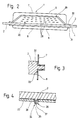
- the housing 1 has a closed plastic frame 2 produced by injection molding. On the top 3 and the bottom 4 of the plastic frame 2, two plastic housing shells 5 and 6 are attached.
- the housing plastic shell 5 forms a trough-shaped, relatively deep upper shell 7 and the housing plastic shell 6 is designed as a trough-shaped but flatter lower shell 8.
- FIG. 1 this has four frame legs 9, 10, 11 and 12 which are integrally connected to one another.
- a heat conducting web 13 of a heat sink 14 is embedded in the frame leg 10.
- the heat conducting web 13 is thus extrusion-coated with plastic during the manufacture of the plastic frame 2.
- the heat conducting web 13 merges at one end 15 into an angled component mounting surface 16.
- the other end 17 of the heat conducting web 13 is connected in one piece to a heat dissipation element 18 located outside the plastic frame 12.
- the heat dissipation elements 18 each have a bore 19 for fastening elements, so that they form fastening connections 20 for the plastic frame 2 and thus for the housing 1.
- molded-on tabs 21 can also be formed on the plastic frame 2, which are provided with mounting holes 22 (see frame leg 12 in FIG. 1). Since the mounting connections 20 and the tabs 21 jump out over the frame periphery, flanges 23 'are formed from these elements, the one enable particularly simple assembly of the housing 1.
- a circuit board 23 is fastened to the frame legs 9, 10, 11 and 12 and has an electronic circuit, preferably control unit electronics (not shown).
- the circuit board 23 is either located inside the frame or it is arranged on the underside 4 of the plastic frame 2 such that no frame parts protrude beyond the underside of the circuit board 23.
- metal pins 24 molded into the plastic frame 2 are provided, which engage in bores 25 of the printed circuit board 23 and hold the latter by bending on the underside of the printed circuit board.
- the bores 25 are assigned metallic / metallized areas, in particular conductor tracks, so that the circuit board is held by the bent metal pins 24 until a soldering process and there is a firm connection between the metal pins 24 and the circuit board 23 after the soldering.
- the printed circuit board 23 may be held on the plastic frame 2 by means of screws.
- a connector plug 26 is provided, which is embedded in the frame leg 11 of the plastic frame 2. It is extrusion-coated with plastic during the manufacture of the plastic frame 2, so that a gap-free seal is ensured.
- the contact tabs 27 of the contacts 28 of the connector 26 are connected in a suitable manner to the electronic circuit arranged on the printed circuit board 23, the latter having heat-generating power components (not shown) which are arranged on the component mounting surface 16 of the heat sink 14 with the lowest possible heat transfer resistance.
- the connector plug 26 it is alternatively also possible for the connector plug 26 to be arranged on the upper side 3 of the plastic frame 2, the upper shell 7 of the housing 1 having a shape-matched edge contour 29 which bears tightly against the upper side of the connector plug 26.
- Upper shell 7 and lower shell 8 have angled edge webs 30 and 31, which are welded all round to the top 3 and the bottom 4 of the plastic frame 2. This is preferably carried out in one operation, namely in the so-called plister process, the two housing plastic shells 5 and 6 being sealed by sealing a suitable tool with a heated tool stamp to the plastic frame 2.
- the plastic housing shells 5 and 6 are provided with a metallization. For this they are either steamed with metal or with equipped with a metal insert. They can be produced using the injection molding process or the deep-drawing process.
- the lower shell 8 is first inserted into a tool, then the plastic frame 2 with the printed circuit board 23 attached to it is placed on the lower shell 8 in a position aligned by suitable joining aids, and finally the housing is completed by applying the upper shell 7.
- printed circuit board blanks are preferably used, on which several plastic frames 2 can be placed, so that several printed circuit boards can simultaneously be moved over a soldering bath by means of the metal pins 24 described above. After soldering, the individual printed circuit boards 23 with the plastic frames 2 attached to them are broken out or punched out of the printed circuit board. This makes the production particularly economical.
- FIG. 3 shows that the plastic frame 2 can be designed step-like in the fastening area with the housing plastic shells 5 and 6.
- the upper shell 7 engages in one stage 32 and the lower shell 8 engages in the other stage 33.
- the connection area between the shells and the frame is thus formed over a particularly large area, so that an absolutely tight connection is produced during welding. Instead of welding, gluing can also take place.
- each snap projection 34 has a web 35 which has a head-shaped end region 36. Head area 36 and web 35 are provided with a slot 37.
- the printed circuit board 23 has bores 38 which are adapted to the diameter of the web 35.
- the holes 38 are pressed onto the snap projections 34, the head-shaped end region 36 being reduced in diameter due to the slot 37, so that the web 35 can engage in the bore 38.
- the end region 36 springs apart again, so that a grip behind the printed circuit board 23 is created.
Abstract
Description
Die Erfindung betrifft ein Gehäuse für eine elektronische , mit Anschlußstecker versehene Schaltung, insbesondere für eine Steuergeräteelektronik einer Brennkraftmaschine eines Fahrzeugs, mit einem Rahmen, an dem eine die elektronische Schaltung aufweisende Leiterplatte befestigt ist, und mit einem Kühlkörper, dem Leistungs-Bauelemente der elektronischen Schaltung zugeordnet sind, sowie mit einer die Leiterplatte umfangenden Abdeckung. Ein derartiges Gehäuse ist aus EP-A-0 335 783 bekannt.The invention relates to a housing for an electronic circuit provided with a connector, in particular for control unit electronics of an internal combustion engine of a vehicle, with a frame to which a circuit board having the electronic circuit is fastened, and with a heat sink, the power components of the electronic circuit are assigned, as well as with a cover encompassing the printed circuit board. Such a housing is known from EP-A-0 335 783.
Gehäuse für elektronische Schaltungen, die Umwelteinflüssen ausgesetzt sind, müssen dicht schliessen. Bekannt sind aufwendige Konstruktionen mit Dichtungseinlagen. Aus der DE-PS 25 46 334 geht ein elektronisches Steuergerät mit einem Gehäuse hervor, das einen Kühlrahmen aufweist. Der Kühlrahmen besitzt einen Boden, auf dem sich erwärmende Bauelemente einer Leistungsstufe befinden. Der Kühlrahmen erfordert ein relativ kompliziert ausgebildetes Metallprofil. Die bekannte Version ist daher recht kostenintensiv. Da der Kühlrahmen von einer haubenartigen Abdeckung überfangen wird, ist bei der Auslegung darauf zu achten, daß die von der Leistungsstufe erzeugte Verlustwärme in einem derartigen Maße abgeführt wird, daß keine unzulässige Erwärmung stattfindet.Housings for electronic circuits that are exposed to environmental influences must close tightly. Elaborate constructions with sealing inserts are known. From DE-PS 25 46 334 an electronic control unit with a housing emerges, which has a cooling frame. The cooling frame has a floor on which there are heating components of a power level. The cooling frame requires a relatively complicated metal profile. The known version is therefore quite expensive. Since the cooling frame is covered by a hood-like cover, care must be taken when designing that the heat loss generated by the power stage is dissipated to such an extent that no inadmissible heating takes place.
Der Erfindungsgegenstand mit den im Hauptanspruch genannten Merkmalen hat demgegenüber den Vorteil, daß bei sehr einfacher, kostengünstiger Ausbildung ein dicht schließendes Gehäuse vorliegt, daß ausgezeichnete Wärmeableiteigenschaften für wärmeerzeugende Bauelemente aufweist. Es besitzt einen gespritzten Kunststoffrahmen, in den mindestens ein Wärmeleitsteg wenigstens eines Kühlkörpers eingeformt ist. Bei der Herstellung wird der Wärmeleitsteg im Kunststoffspritzverfahren eingebettet, so daß eine spaltfreie und dichte Ausbildung gewährleistet ist. Das eine Ende des Wärmeleitstegs geht in eine im Gehäuseinneren liegende Bauelement-Montagefläche über und das andere Ende des Wärmeleitstegs ist als außerhalb des Gehäuses liegendes Wärmeabführelement ausgebildet. Die von auf der Bauelement-Montagefläche angeordneten Bauelementen erzeugte Wärme wird daher direkt über den eingebetteten Wärmeleitsteg aus dem Gehäuseinneren herausgeführt, so daß ausgezeichnete Kühleigenschaften vorliegen. Außerhalb des Gehäuses erfolgt eine Wärmeableitung durch das Wärmeabführelement, wobei vorzugsweise eine Einstückigkeit zwischen Bauelement-Montagefläche, Wärmeleitsteg und Wärmeabführelement vorliegt, so daß extrem kleine Wärmeübergangswiderstände vorliegen. Trotz eines dicht schließenden Gehäuses ist auf die genannte Art und Weise eine besonders effektive Wärmeabfuhr gewährleistet. Der Kunststoffrahmen stellt dabei eine besonders einfache und kostengünstige Lösung dar. Der Kühlkörper besteht vorzugsweise aus Metall.The subject of the invention with the features mentioned in the main claim has the advantage that with a very simple, inexpensive design, there is a tightly fitting housing that has excellent heat dissipation properties for heat-generating components. It has an injection-molded plastic frame into which at least one heat-conducting web of at least one heat sink is molded. During manufacture, the heat conducting web is embedded in the plastic injection molding process, so that a gap-free and tight design is ensured. One end of the heat conducting web merges into a component mounting surface located inside the housing and the other end of the heat conducting web is designed as a heat dissipation element located outside the housing. The heat generated by components arranged on the component mounting surface is therefore directly above the embedded one Thermal conductor led out of the interior of the housing, so that excellent cooling properties are available. Outside the housing, heat is dissipated through the heat dissipation element, preferably in one piece between the component mounting surface, the heat conducting web and the heat dissipation element, so that extremely small heat transfer resistances are present. Despite a tightly fitting housing, particularly effective heat dissipation is ensured in the manner mentioned. The plastic frame represents a particularly simple and inexpensive solution. The heat sink is preferably made of metal.
Eine Doppelfunktion wird vom Wärmeabführelement übernommen, wenn dieses gleichzeitig als Gehäuse-Befestigungsanschluß ausgebildet ist. Überdies werden hierdurch die Wärmeableiteigenschaften noch weiter verbessert, da über die Befestigung die vom Wärmeleitsteg transportierte Wärme aufgenommen bzw. weitergeleitet wird, so daß Wärmestaus vermieden sind.A double function is taken over by the heat dissipation element if it is simultaneously designed as a housing attachment connection. In addition, the heat dissipation properties are hereby further improved, since the heat transported by the heat conducting web is absorbed or transmitted via the fastening, so that heat accumulations are avoided.
Insbesondere ist der Gehäuse-Befestigungsanschluß ein mit einer Bohrung für ein Befestigungselement versehener Flansch. Die dem Flansch zugeführte Wärme kann daher über das Befestigungselement an eine Tragkonstruktion oder dergleichen weitergegeben werden. Sofern das Gehäuse eine Steuergeräteelektronik für eine Brennkraftmaschine aufnimmt, wird die von entsprechenden Leistungshalbleitern erzeugte Wärme über z.B. als Gewindeschrauben ausgebildete Befestigungselemente zum Chassis oder zur Karosserie des Kraftfahrzeugs abgeleitet. Dieses führt zu ausgezeichneten Kühlungseigenschaften. Da die elektronische Schaltung an Versorgungs- und Datenleitungen angeschlossen werden muß, ist ein Anschlußstecker vorgesehen. Dieser läßt sich auf besonders einfache Weise dadurch am Gehäuse festlegen, wenn er in den Kunststoffrahmen eingeformt ist. Mithin wird bei der Rahmenherstellung nicht nur der Wärmeleitsteg des Kühlkörpers, sondern auch der Anschlußstecker mit Kunststoff umspritzt. Damit ist auch beim Anschlußstecker ein spaltfreier Übergang zum Kunststoffrahmen garantiert.In particular, the housing fastening connection is a flange provided with a bore for a fastening element. The heat supplied to the flange can therefore be passed on to a supporting structure or the like via the fastening element. If the housing accommodates control unit electronics for an internal combustion engine, the heat generated by the corresponding power semiconductors is dissipated to the chassis or body of the motor vehicle via, for example, fastening elements designed as threaded screws. This leads to excellent cooling properties. Since the electronic circuit must be connected to supply and data lines, a connector is provided. This can be fixed in a particularly simple manner on the housing when it is molded into the plastic frame. Thus, not only the heat sink of the heat sink, but also the connector is overmolded with plastic during frame production. This guarantees a gap-free transition to the plastic frame even with the connector.
Nach einer bevorzugten Ausführungsform der Erfindung weist der Kunststoffrahmen angespritzte Schnappvorsprünge auf, die in Bohrungen der Leiterplatte einrastbar sind. Die Festlegung der Leiterplatte kann somit am Kunststoffrahmen durch eine einfache Rastverbindung erfolgen. Die Leiterplatte wird bei der Montage den einstückig mit dem Kunststoffrahmen ausgebildeten Schnappvorsprüngen derart zugeordnet, daß letztere mit den Bohrungen fluchten. Anschließend erfolgt die Verrastung. Es ist auch denkbar, daß entsprechend ausgebildete Schnappvorsprünge hinter die umlaufende Randkante der Leiterplatte greifen.According to a preferred embodiment of the invention, the plastic frame has molded-on snap projections which can be snapped into holes in the printed circuit board. The circuit board can thus be fixed to the plastic frame by a simple snap connection. The circuit board is assigned to the snap projections formed in one piece with the plastic frame during assembly such that the latter are aligned with the bores. Then the locking takes place. It is also conceivable that appropriately designed snap projections engage behind the peripheral edge of the circuit board.
Zusätzlich oder alternativ kann die Leiterplatte auch durch in den Kunststoffrahmen eingeformte Metallstifte gehalten werden, die in Bohrungen der Leiterplatte eingreifen. Die Metallstifte sind vorzugsweise derart abgebogen, daß ein Herausrutschen aus den Bohrungen verhindert ist. Eine besonders haltbare Verbindung ergibt sich dann, wenn die Metallstifte die Leiterplatte vorzugsweise bis zum Leiterplattenlötvorgang aufgrund ihrer Abbiegungen halten und daß anschließend durch den Lötvorgang eine halternde Lötverbindung zwischen den Stiften und der Leiterplatte hergestellt wird. Hierzu weisen die Bohrungen der Leiterplatte vorzugsweise metallische oder metallisierte Bereiche, insbesondere Leiterbahnen auf, so daß eine hochbelastbare Lötverbindung ausgebildet werden kann.Additionally or alternatively, the circuit board can also be held by metal pins molded into the plastic frame, which engage in holes in the circuit board. The metal pins are preferably bent so that slipping out of the holes is prevented. A particularly durable connection is obtained when the metal pins, preferably up to Hold PCB soldering process due to their bends and that subsequently a holding solder connection between the pins and the circuit board is made by the soldering process. For this purpose, the holes in the circuit board preferably have metallic or metallized areas, in particular conductor tracks, so that a highly loadable soldered connection can be formed.
Die Abdeckung ist vorzugsweise von zwei GehäuseKunststoffschalen gebildet, die mit der Ober- und Unterseite des Kunststoffrahmens verbunden, vorzugsweise verschweißt, sind. Durch die Verschweissung ist auf besonders einfache Weise ein dicht schließendes Gehäuse realisiert. In einem Arbeitsgang kann z.B. im Plisterverfahren eine Verschweissung erfolgen, wobei die beiden Gehäuse-Kunststoffschalen durch Schließen entsprechender Werkzeuge und Beheizen der Werkzeugstempel mit dem Kunststoffrahmen verbunden werden.The cover is preferably formed by two housing plastic shells which are connected, preferably welded, to the top and bottom of the plastic frame. A sealed housing is realized in a particularly simple manner by the welding. In one operation, e.g. Welding is carried out in the plistering process, the two plastic housing shells being connected to the plastic frame by closing appropriate tools and heating the tool stamp.
Um eine hohe elektromagnetische Verträglichkeit (EMV) zu erzielen, so daß weder von der elektronischen Schaltung eine Störabstrahlung nach außen, noch eine Störeinstrahlung nach innen erfolgen kann, sind die Gehäuse-Kunststoffschalen vorzugsweise metallisiert.In order to achieve a high level of electromagnetic compatibility (EMC), so that neither interference from the electronic circuit can radiate to the outside nor interference to the inside, the plastic housing shells are preferably metallized.
Die Erfindung wird im folgenden anhand der Figuren näher erläutert. Es zeigen:
- Figur 1 eine perspektivische Ansicht eines aus Kunststoff bestehenden Gehäuserahmens, an dem eine Leiterplatte befestigt ist und der einen eingeformten Kühlkörper sowie einen eingeformten Anschlußstecker aufweist,
Figur 2 eine Seitenansicht eines erfindungsgemäßen Gehäuses mit einer aus zwei Kunststoffschalen bestehenden Abdeckung,Figur 3 eine Detail-Schnittansicht der Befestigungszone der Gehäuse-Kunststoffschalen am Kunststoffrahmen und- Figur 4 einen mit Schnappvorsprung ausgebildeten Kunststoffrahmenabschnitt zur Befestigung der Leiterplatte.
- 1 shows a perspective view of a housing frame made of plastic, to which a printed circuit board is fastened and which has a molded-in heat sink and a molded-in connector,
- FIG. 2 shows a side view of a housing according to the invention with a cover consisting of two plastic shells,
- Figure 3 is a detailed sectional view of the fastening zone of the plastic housing shells on the plastic frame and
- FIG. 4 shows a plastic frame section designed with a snap projection for fastening the printed circuit board.
Das erfindungsgemäße Gehäuse 1 weist gemäß der Figuren 1 und 2 einen geschlossenen, in Spritztechnik hergestellten Kunststoffrahmen 2 auf. Auf der Oberseite 3 sowie der Unterseite 4 des Kunststoffrahmens 2 sind zwei Gehäuse-Kunststoffschalen 5 und 6 befestigt. Die Gehäuse-Kunststoffschale 5 bildet eine wannenförmige, relativ tiefe Oberschale 7 und die Gehäuse-Kunststoffschale 6 ist als ebenfalls wannenförmige, jedoch flachere Unterschale 8 ausgebildet.According to FIGS. 1 and 2, the housing 1 according to the invention has a closed
Im nachfolgenden soll zunächst auf den Kunststoffrahmen 2 eingegangen werden. Dieser besitzt gemäß Figur 1 vier einstückig miteinander verbundene Rahmenschenkel 9, 10, 11 und 12. In den Rahmenschenkel 10 ist ein Wärmeleitsteg 13 eines Kühlkörpers 14 eingebettet. Der Wärmeleitsteg 13 wird also bei der Herstellung des Kunststoffrahmens 2 mit Kunststoff umspritzt. Im Rahmeninneren geht der Wärmeleitsteg 13 an seinem einen Ende 15 in eine abgewinkelte Bauelement-Montagefläche 16 über. Das andere Ende 17 des Wärmeleitstegs 13 ist einstückig mit einem außerhalb des Kunststoffrahmens 12 gelegenen Wärmeabführelement 18 verbunden. Der im Ausführungs- beispiel der Figur 1 gezeigte Kühlkörper 14 besitzt zwei jeweils zu der Bauelement-Montagefläche 16 führende Wärmeleitstege 13, die beide in den Rahmenschenkel 10 eingeformt sind und an ihren Enden 17 jeweils ein Wärmeabführelement 18 aufweisen. Die Wärmeabführelemente 18 besitzen jeweils eine Bohrung 19 für Befestigungselemente, so daß sie Befestigungsanschlüsse 20 für den Kunststoffrahmen 2 und damit für das Gehäuse 1 bilden. Mittels geeigneter Befestigungselemente, die in die Bohrungen 19 eingreifen, kann eine Festlegung an einem geeigneten Montageort erfolgen.In the following, the
Für eine Befestigung können am Kunststoffrahmen 2 ferner angespritzte Laschen 21 ausgebildet sein, die mit Befestigungsbohrungen 22 versehen sind (siehe Rahmenschenkel 12 in Figur 1). Da die Befestigungsanschlüsse 20 und auch die Laschen 21 über die Rahmenperipherie herausspringen, werden von diesen Elementen Flansche 23′ gebildet, die eine besonders einfache Montage des Gehäuses 1 ermöglichen.For attachment, molded-on
An den Rahmenschenkeln 9, 10, 11 und 12 ist eine Leiterplatte 23 befestigt, die eine elektronische Schaltung, vorzugsweise eine Steuergeräteelektronik, aufweist (nicht dargestellt). Die Leiterplatte 23 befindet sich entweder im Rahmeninneren oder sie wird derart an der Unterseite 4 des Kunststoffrahmens 2 angeordnet, daß keine Rahmenteile über die Unterseite der Leiterplatte 23 hinausragen. Zur Befestigung sind in den Kunststoffrahmen 2 eingeformte Metallstifte 24 vorgesehen, die in Bohrungen 25 der Leiterplatte 23 eingreifen und letztere durch an der Unterseite der Leiterplatte erfolgendes Abbiegen halten. Den Bohrungen 25 sind metallische/metallisierte Bereiche, insbesondere Leiterbahnen zugeordnet, so daß bis zu einem Lötvorgang die Leiterplatte durch die umgebogenen Metallstifte 24 gehalten ist und nach dem Löten eine feste Verbindung zwischen den Metallstiften 24 und der Leiterplatte 23 besteht.A
Alternativ ist es jedoch auch möglich, daß die Leiterplatte 23 mittels Schrauben an dem Kunststoffrahmen 2 gehaltert ist.Alternatively, however, it is also possible for the printed
Da die elektronische Schaltung der Leiterplatte 23 an Versorgungs- und Datenleitungen angeschlossen werden muß, ist ein Anschlußstecker 26 vorgesehen, der in den Rahmenschenkel 11 des Kunststoffrahmens 2 eingebettet ist. Er wird bei der Herstellung des Kunststoffrahmens 2 mit Kunststoff umspritzt, so daß eine spaltfreie Abdichtung gewährleistet ist. Die Kontaktfahnen 27 der Kontakte 28 des Anschlußsteckers 26 sind in geeigneter Weise mit der auf der Leiterplatte 23 angeordneten elektronischen Schaltung verbunden, Letztere weist wärmeerzeugende Leistungs-Bauelemente auf (nicht dargestellt), die auf der Bauelement-Montagefläche 16 des Kühlkörpers 14 mit möglichst geringem Wärmeübergangswiderstand angeordnet sind.Since the electronic circuit of the
Gemäß Figur 2 ist es alternativ auch möglich, daß der Anschlußstecker 26 auf der Oberseite 3 des Kunststoffrahmens 2 angeordnet ist, wobei die Oberschale 7 des Gehäuses 1 eine formangepaßte Randkontur 29 aufweist, die dichtschließend an der Oberseite des Anschlußsteckers 26 anliegt.According to FIG. 2, it is alternatively also possible for the
Oberschale 7 und Unterschale 8 weisen abgewinkelte Randstege 30 bzw. 31 auf, die mit der Oberseite 3 bzw. der Unterseite 4 des Kunststoffrahmens 2 umlaufend verschweißt sind. Dieses wird bevorzugt in einem Arbeitsgang, und zwar im sogenannten Plisterverfahren, durchgeführt, wobei die beiden Gehäuse-Kunststoffschalen 5 und 6 durch Schließen eines geeigneten Werkzeugs mit beheiztem Werkzeug stempel mit dem Kunststoffrahmen 2 dicht verschweißt werden.
Zur Erzielung einer hohen elektromagnetischen Verträglichkeit sind die Gehäuse-Kunststoffschalen 5 und 6 mit einer Metallisierung versehen. Hierzu werden sie entweder mit Metall bedampft oder mit einer Metalleinlage ausgestattet. Sie können im Spritzverfahren oder im Tiefziehverfahren hergestellt sein.To achieve high electromagnetic compatibility, the
Bei der Montage wird zunächst die Unterschale 8 in ein Werkzeug eingelegt, dann wird der Kunststoffrahmen 2 mit der an ihm befestigten Leiterplatte 23 in durch geeignete Fügehilfen ausgerichteter Position an die Unterschale 8 angelegt und schließlich das Gehäuse durch Aufbringen der Oberschale 7 komplettiert.During assembly, the
Bei der Herstellung der Rahmen/Leiterplatteneinheit werden vorzugsweise sogenannte Leiterplattennutzen verwendet, auf denen mehrere Kunststoffrahmen 2 Platz finden, so daß gleichzeitig mehrere Leiterplatten mittels der zuvor beschriebenen Metallstifte 24 gleichzeitig über ein Lötbad gefahren werden können. Nach dem Verlöten werden aus den Leiterplattennutzen die einzelnen Leiterplatten 23 mit den daran befestigten Kunststoffrahmen 2 herausgebrochen oder herausgestanzt. Die Herstellung wird dadurch besonders wirtschaftlich.In the manufacture of the frame / printed circuit board unit, so-called printed circuit board blanks are preferably used, on which several
Die Figur 3 zeigt, daß der Kunststoffrahmen 2 im Befestigungsbereich mit den Gehäuse-Kunststoffschalen 5 und 6 stufenförmig ausgebildet sein kann. In die eine Stufe 32 greift die Oberschale 7 und in die andere Stufe 33 die Unterschale 8 ein. Der Verbindungsbereich zwischen den Schalen und dem Rahmen wird dadurch besonders großflächig ausgebildet, so daß bei der Schweißung eine absolut dichte Verbindung entsteht. Es kann auch anstatt der Schweißung eine Verklebung erfolgen.FIG. 3 shows that the
Alternativ zu den bereits beschriebenen Leiterplattenfestlegungen ist es gemäß Figur 4 auch möglich, daß der Kunststoffrahmen 2 einstückig angespritzte Schnappvorsprünge 34 aufweist. Jeder Schnappvorsprung 34 weist einen Steg 35 auf, der einen kopfförmigen Endbereich 36 besitzt. Kopfbereich 36 und Steg 35 sind mit einem Schlitz 37 versehen. Die Leiterplatte 23 weist dem Durchmesser des Stegs 35 angepaßte Bohrungen 38 auf. Für die Befestigung der Leiterplatte 23 wird diese mit ihren Bohrungen 38 auf die Schnappvorsprünge 34 gedrückt, wobei aufgrund des Schlitzes 37 der kopfförmige Endbereich 36 seinen Durchmesser verkleinert, so daß der Steg 35 in die Bohrung 38 eingreifen kann. Im aufgesteckten Zustand federt der Endbereich 36 wieder auseinander, so daß ein Hintergriff zur Leiterplatte 23 entsteht.As an alternative to the circuit board specifications already described, it is also possible, as shown in FIG. 4, for the
Claims (9)
- Housing (1) for an electronic circuit provided with a connector plug (26), in particular for control electronics of an internal combustion engine of a vehicle, having a frame (2) to which a printed circuit board (23) which has the electronic circuit is attached, and having a cooling element (14) to which power components of the electronic circuit are assigned, and having a cover (5, 6) which surrounds the printed circuit board, characterized in that the frame is constructed as an injection-moulded plastic frame (2) with at least one formed-in heat conducting web (13) of the cooling element (14), one end (15) of the heat conducting web (13) merging with a component mounting face (16) which is located in the interior of the housing and the other end (17) of the heat conducting web (13) being constructed as an element (18) for conducting away heat which is located outside the housing (1).
- Housing according to Claim 1, characterized in that the element (18) for conducting away heat is constructed as a housing-attachment connection (20).
- Housing according to Claim 2, characterized in that the housing-attachment connection (20) is a flange (23′) provided with a bore (19) for an attachment element.
- Housing according to one of the preceding claims, characterized in that the connector plug (26) is formed into the plastic frame (2).
- Housing according to one of the preceding claims, characterized in that the plastic frame (2) has snap-in projections (34) which are injection-moulded on and can be engaged in bores (38) of the printed circuit board (23).
- Housing according to one of the preceding claims, characterized by metal pins (24) which are formed into the plastic frame (2) and engage in bores (25) of the printed circuit board (23) and hold them by bending.
- Housing according to Claim 6, characterized in that the metal pins (24) hold the printed circuit board (23) by bending preferably until the soldering process for the printed circuit board, and in that the bores (25) of the printed circuit board (23) are assigned metallic/metallized regions, in particular conductor tracks, in such a way that after the soldering process a securing solder connection exists between the metal pins (24) and the printed circuit board (23).
- Housing according to one of the preceding claims, characterized in that the cover is formed by two plastic housing shells (5, 6) which are connected, in particular fused, to the upper side and underside (3, 4) of the plastic frame (2).
- Housing according to Claim 8, characterized in that the plastic housing shells (5, 6) are metallized.
Applications Claiming Priority (3)
| Application Number | Priority Date | Filing Date | Title |
|---|---|---|---|
| DE3933123 | 1989-10-04 | ||
| DE3933123A DE3933123A1 (en) | 1989-10-04 | 1989-10-04 | HOUSING FOR AN ELECTRONIC CIRCUIT |
| PCT/DE1990/000741 WO1991005451A1 (en) | 1989-10-04 | 1990-09-28 | Housing for an electronic circuit |
Publications (2)
| Publication Number | Publication Date |
|---|---|
| EP0446323A1 EP0446323A1 (en) | 1991-09-18 |
| EP0446323B1 true EP0446323B1 (en) | 1994-07-13 |
Family
ID=6390813
Family Applications (1)
| Application Number | Title | Priority Date | Filing Date |
|---|---|---|---|
| EP90914067A Expired - Lifetime EP0446323B1 (en) | 1989-10-04 | 1990-09-28 | Housing for an electronic circuit |
Country Status (5)
| Country | Link |
|---|---|
| US (1) | US5118903A (en) |
| EP (1) | EP0446323B1 (en) |
| JP (1) | JP2930135B2 (en) |
| DE (2) | DE3933123A1 (en) |
| WO (1) | WO1991005451A1 (en) |
Cited By (1)
| Publication number | Priority date | Publication date | Assignee | Title |
|---|---|---|---|---|
| DE102004029536A1 (en) * | 2004-06-18 | 2006-01-05 | Robert Bosch Gmbh | Pin for electrically connecting an inner surface of a metallized plastic housing to a component comprises a connecting section, a fixing section and a contact section for cold electrical contact of the metallized surface |
Families Citing this family (21)
| Publication number | Priority date | Publication date | Assignee | Title |
|---|---|---|---|---|
| DE4215041C3 (en) * | 1991-05-22 | 1997-09-25 | Siemens Ag | Electronic control unit |
| US5237486A (en) * | 1992-06-05 | 1993-08-17 | Apple Computer, Inc. | Structural frame for portable computer |
| GB9308060D0 (en) * | 1993-04-19 | 1993-06-02 | Cancer Res Campaign Tech | Stem cell inhibitor |
| US5455741A (en) * | 1993-10-26 | 1995-10-03 | Pulse Engineering, Inc. | Wire-lead through hole interconnect device |
| JP3051011B2 (en) * | 1993-11-18 | 2000-06-12 | 株式会社東芝 | Power module |
| DE4445125A1 (en) | 1994-12-17 | 1996-06-20 | Wabco Gmbh | Housing for an electrical component |
| US5586005A (en) * | 1995-03-16 | 1996-12-17 | International Business Machines Corporation | Removable heat sink assembly for a chip package |
| US6005463A (en) * | 1997-01-30 | 1999-12-21 | Pulse Engineering | Through-hole interconnect device with isolated wire-leads and component barriers |
| DE19703676C2 (en) | 1997-01-31 | 2002-01-24 | Siemens Ag | Method and device for the precise tolerance connection of two components |
| JP3248480B2 (en) * | 1998-01-22 | 2002-01-21 | 住友電装株式会社 | Distribution box |
| US6055158A (en) * | 1999-03-16 | 2000-04-25 | Framatome Connectors Interlock, Inc. | Electronic component heat sink assembly |
| TW420969B (en) * | 2000-01-28 | 2001-02-01 | Metal Ind Redearch & Dev Ct | Method of producing thin metal case with joint element |
| DE10020018A1 (en) | 2000-04-22 | 2001-11-08 | Brose Fahrzeugteile | Electromechanical drive device |
| US6377462B1 (en) | 2001-01-09 | 2002-04-23 | Deere & Company | Circuit board assembly with heat sinking |
| DE10247828B4 (en) * | 2002-10-14 | 2005-03-03 | Siemens Ag | Heat dissipating and radiating plastic housing with cooling / support ribs and molded heat sink and method for its production |
| DE102006006846B3 (en) * | 2006-02-15 | 2007-08-30 | Tyco Electronics Amp Gmbh | Electric power distributor and electric punched grid therefor |
| EP2040524A1 (en) * | 2007-09-24 | 2009-03-25 | Siemens Aktiengesellschaft | Method for manufacturing an electronic device, in particular a power module, electrical device and connecting contact |
| JP5184286B2 (en) * | 2008-09-30 | 2013-04-17 | 富士通テン株式会社 | Housing fixing structure |
| JP6310791B2 (en) * | 2014-06-25 | 2018-04-11 | 矢崎総業株式会社 | Switch box |
| CN105140170B (en) * | 2015-08-31 | 2017-12-22 | 北京航天控制仪器研究所 | A kind of more ceramic cartridge sealing cap fixtures of achievable fine alignment |
| DE102019203017A1 (en) * | 2019-03-06 | 2020-09-10 | Robert Bosch Gmbh | Component arrangement with a connection between two components |
Family Cites Families (12)
| Publication number | Priority date | Publication date | Assignee | Title |
|---|---|---|---|---|
| US3869563A (en) * | 1973-09-27 | 1975-03-04 | Motorola Inc | Encapsulation housing for electronic circuit boards or the like and method of encapsulating |
| US3904262A (en) * | 1974-09-27 | 1975-09-09 | John M Cutchaw | Connector for leadless integrated circuit packages |
| DE2546334C2 (en) * | 1975-10-16 | 1984-10-11 | Robert Bosch Gmbh, 7000 Stuttgart | Electronic control unit |
| DE3020902A1 (en) * | 1980-06-02 | 1981-12-17 | Robert Bosch Gmbh, 7000 Stuttgart | ELECTRONIC CONTROL UNIT, IN PARTICULAR FOR MOTOR VEHICLES |
| US4679118A (en) * | 1984-08-07 | 1987-07-07 | Aavid Engineering, Inc. | Electronic chip-carrier heat sinks |
| GB2197755B (en) * | 1986-08-20 | 1990-05-09 | Plessey Co Plc | Electronic circuit housing |
| US5019940A (en) * | 1987-02-24 | 1991-05-28 | Thermalloy Incorporated | Mounting apparatus for electronic device packages |
| US4811165A (en) * | 1987-12-07 | 1989-03-07 | Motorola, Inc. | Assembly for circuit modules |
| FR2629665B1 (en) * | 1988-03-30 | 1991-01-11 | Bendix Electronics Sa | ELECTRONIC CIRCUIT BOX |
| FR2634617A1 (en) * | 1988-07-22 | 1990-01-26 | Neiman Sa | Fitted electronic module |
| DE3837974A1 (en) * | 1988-11-09 | 1990-05-10 | Telefunken Electronic Gmbh | ELECTRONIC CONTROL UNIT |
| JP2612339B2 (en) * | 1989-04-18 | 1997-05-21 | 三菱電機株式会社 | Electronic equipment housing |
-
1989
- 1989-10-04 DE DE3933123A patent/DE3933123A1/en not_active Withdrawn
-
1990
- 1990-09-28 WO PCT/DE1990/000741 patent/WO1991005451A1/en active IP Right Grant
- 1990-09-28 DE DE59006436T patent/DE59006436D1/en not_active Expired - Fee Related
- 1990-09-28 EP EP90914067A patent/EP0446323B1/en not_active Expired - Lifetime
- 1990-09-28 JP JP2513114A patent/JP2930135B2/en not_active Expired - Lifetime
- 1990-09-28 US US07/679,031 patent/US5118903A/en not_active Expired - Fee Related
Cited By (1)
| Publication number | Priority date | Publication date | Assignee | Title |
|---|---|---|---|---|
| DE102004029536A1 (en) * | 2004-06-18 | 2006-01-05 | Robert Bosch Gmbh | Pin for electrically connecting an inner surface of a metallized plastic housing to a component comprises a connecting section, a fixing section and a contact section for cold electrical contact of the metallized surface |
Also Published As
| Publication number | Publication date |
|---|---|
| DE59006436D1 (en) | 1994-08-18 |
| JPH04502090A (en) | 1992-04-09 |
| EP0446323A1 (en) | 1991-09-18 |
| WO1991005451A1 (en) | 1991-04-18 |
| JP2930135B2 (en) | 1999-08-03 |
| DE3933123A1 (en) | 1991-04-11 |
| US5118903A (en) | 1992-06-02 |
Similar Documents
| Publication | Publication Date | Title |
|---|---|---|
| EP0446323B1 (en) | Housing for an electronic circuit | |
| EP1208618B1 (en) | Control device and soldering method | |
| EP0588793B1 (en) | Housing for motor vehicle electronics | |
| DE10134639B4 (en) | Housing for an electronic control unit in vehicles | |
| EP0712265B1 (en) | Electronic assembly | |
| DE10392749B4 (en) | Control module housing for a vehicle | |
| EP1697175B1 (en) | Control unit and method for producing the same | |
| AT503687B1 (en) | CONTROL UNIT WITH A HEAD-SIDED CONTACTING CIRCUIT | |
| DE102006016775A1 (en) | Electronic device and method for making the same | |
| EP0446320B1 (en) | Housing for an electronic circuit | |
| DE3936906A1 (en) | Housing for electronic device in motor vehicle - has frame provided by inside surface fitted with two opposing carrier plates | |
| EP0708583A1 (en) | Electronic apparatus and its manufacture | |
| DE102008051545B4 (en) | Multi-contact electronic device and method of making the same | |
| EP0717588A2 (en) | Casing for an electrical device | |
| DE10304889A1 (en) | Electronic circuit board housing and method for producing an electronic circuit unit | |
| EP0526466B1 (en) | Electric switching and control device, in particular for motor vehicles | |
| EP1586223B1 (en) | Electrical connection element, especially for electric tool switches | |
| EP1282345B1 (en) | Housing for board with electronic components in vehicle | |
| DE10205816A1 (en) | Housing for electrical device e.g. control circuitry in motor vehicle, has contact spring which makes contact with grounded surface of circuit board when device is assembled | |
| DE102005053973A1 (en) | sensor assembly | |
| DE102017210176A1 (en) | electronic module | |
| DE3933124A1 (en) | ELECTRONIC DEVICE WITH FLEXIBLE PCB AREA | |
| EP2514285B1 (en) | End element for a housing | |
| EP0728405B1 (en) | Device for removing heat dissipated by an electronic or electro-mechanical component | |
| DE102012105352A1 (en) | positioning |
Legal Events
| Date | Code | Title | Description |
|---|---|---|---|
| PUAI | Public reference made under article 153(3) epc to a published international application that has entered the european phase |
Free format text: ORIGINAL CODE: 0009012 |
|
| 17P | Request for examination filed |
Effective date: 19910507 |
|
| AK | Designated contracting states |
Kind code of ref document: A1 Designated state(s): DE FR GB IT |
|
| RAP3 | Party data changed (applicant data changed or rights of an application transferred) |
Owner name: ROBERT BOSCH GMBH |
|
| 17Q | First examination report despatched |
Effective date: 19931130 |
|
| GRAA | (expected) grant |
Free format text: ORIGINAL CODE: 0009210 |
|
| AK | Designated contracting states |
Kind code of ref document: B1 Designated state(s): DE FR GB IT |
|
| ET | Fr: translation filed | ||
| REF | Corresponds to: |
Ref document number: 59006436 Country of ref document: DE Date of ref document: 19940818 |
|
| ITF | It: translation for a ep patent filed |
Owner name: STUDIO JAUMANN |
|
| GBT | Gb: translation of ep patent filed (gb section 77(6)(a)/1977) |
Effective date: 19940919 |
|
| PLBE | No opposition filed within time limit |
Free format text: ORIGINAL CODE: 0009261 |
|
| STAA | Information on the status of an ep patent application or granted ep patent |
Free format text: STATUS: NO OPPOSITION FILED WITHIN TIME LIMIT |
|
| 26N | No opposition filed | ||
| PGFP | Annual fee paid to national office [announced via postgrant information from national office to epo] |
Ref country code: GB Payment date: 20000911 Year of fee payment: 11 |
|
| PGFP | Annual fee paid to national office [announced via postgrant information from national office to epo] |
Ref country code: FR Payment date: 20000921 Year of fee payment: 11 |
|
| PGFP | Annual fee paid to national office [announced via postgrant information from national office to epo] |
Ref country code: DE Payment date: 20001129 Year of fee payment: 11 |
|
| PG25 | Lapsed in a contracting state [announced via postgrant information from national office to epo] |
Ref country code: GB Free format text: LAPSE BECAUSE OF NON-PAYMENT OF DUE FEES Effective date: 20010928 |
|
| REG | Reference to a national code |
Ref country code: GB Ref legal event code: IF02 |
|
| PG25 | Lapsed in a contracting state [announced via postgrant information from national office to epo] |
Ref country code: DE Free format text: LAPSE BECAUSE OF NON-PAYMENT OF DUE FEES Effective date: 20020501 |
|
| GBPC | Gb: european patent ceased through non-payment of renewal fee |
Effective date: 20010928 |
|
| PG25 | Lapsed in a contracting state [announced via postgrant information from national office to epo] |
Ref country code: FR Free format text: LAPSE BECAUSE OF NON-PAYMENT OF DUE FEES Effective date: 20020531 |
|
| REG | Reference to a national code |
Ref country code: FR Ref legal event code: ST |
|
| PG25 | Lapsed in a contracting state [announced via postgrant information from national office to epo] |
Ref country code: IT Free format text: LAPSE BECAUSE OF NON-PAYMENT OF DUE FEES Effective date: 20050928 |