EP0444816A2 - Circuit element measuring method and apparatus - Google Patents
Circuit element measuring method and apparatus Download PDFInfo
- Publication number
- EP0444816A2 EP0444816A2 EP91301343A EP91301343A EP0444816A2 EP 0444816 A2 EP0444816 A2 EP 0444816A2 EP 91301343 A EP91301343 A EP 91301343A EP 91301343 A EP91301343 A EP 91301343A EP 0444816 A2 EP0444816 A2 EP 0444816A2
- Authority
- EP
- European Patent Office
- Prior art keywords
- terminal
- detection amplifier
- measuring
- zero detection
- voltage
- Prior art date
- Legal status (The legal status is an assumption and is not a legal conclusion. Google has not performed a legal analysis and makes no representation as to the accuracy of the status listed.)
- Withdrawn
Links
Images
Classifications
-
- G—PHYSICS
- G01—MEASURING; TESTING
- G01R—MEASURING ELECTRIC VARIABLES; MEASURING MAGNETIC VARIABLES
- G01R31/00—Arrangements for testing electric properties; Arrangements for locating electric faults; Arrangements for electrical testing characterised by what is being tested not provided for elsewhere
- G01R31/50—Testing of electric apparatus, lines, cables or components for short-circuits, continuity, leakage current or incorrect line connections
Definitions
- the present invention relates to a method and apparatus for high accuracy circuit element measurements by easily correcting changes, if any, in the measurement cables or range resistance.
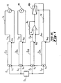
- FIG. 1 is a schematic circuit diagram showing a circuit element measuring apparatus for four-terminal pair measurements according to the prior art.
- a circuit element to be measured (hereinafter referred to as a "DUT" or element Z x ) is connected to a signal source SS, a volt meter VM, a range resistance R r and a zero detection amplifier A which together form a measuring apparatus.
- the impedance value of the element Z x shall also be referred to as Z x .
- the lines CL1, CL2, CL3 and CL4 are generally made of coaxial cables although not limited thereto, and their outer conductor terminals g11, g21, g31 and g41 at one end thereof are connected to one another and held at the same potential.
- the terminals l11 and l21 of the center conductor of the lines CL1 and CL2 at the same end thereof are connected to one terminal of the element Z x .
- the terminals l31 and l41 of CL3 and CL4 are connected to the other terminal of the element Z x .
- the terminals of the center conductors of the lines CL1, CL2, CL3 and CL4 and the outer conductor at the opposite end are respectively designated as l12, g12, l22, g22, l32, g32, l42 and g42.
- the signal source SS and a signal source resistance R s are connected in series.
- the volt meter VM is connected between the terminals l22 and g22.
- the terminals l32 and g32 are respectively connected to the inverted input terminal and non-inverted input terminal of the zero detection amplifier A.
- the feedback resistance R f is connected between the inverted input terminal and the output terminal of the zero detection amplifier A.
- the output of the zero detection amplifier A is introduced into a narrow-band amplification/phase compensation amplifier NBA.
- the output of the NBA is applied through the range resistance R r to the terminal l42.
- the NBA is similar to that used in the aforementioned meters 4274A and 4275A.
- the range resistance R r is placed between the terminal 142 and the NBA output, and the terminals g42 and g32 are also connected.
- an automatic control is performed on the voltage between the terminals l32 and g32, i.e., controlled such that the current flow through the terminal l32 may be substantially zero.
- a voltage V x to be applied to the element Z x is obtained as the indication of the volt meter VM.
- a current I x to flow through the element Z x is obtained as an indication of the range resistance R r .
- the method of measuring the complex voltage or current is well known in the art and is used together with the overall operations of the meter in the aforementioned 4274A or 4275A.
- the calibrations are carried out by the known method of replacing the measured element with a "short” or “open” or by using a known third impedance.
- the range resistance R r is selected to have a magnitude close to that of the Z x . This provides the advantage of a uniform dynamic range for succeeding volt meters by making the magnitudes of the V x and V i same.
- the stabilization of the automatic control loop composed of the line CL3, the zero detection amplifier A, the NBA, the range resistance R r and the line CL4 can be made excellent by selecting a sufficiently small value of the feedback resistance R f .
- Fig. 2 wherein a noise model of the automatic control loop of Fig. 1 is shown so as to provide an understanding of the problem of noise in the prior art thus far described.
- reference characters E1, and E2 designate the thermal noise of the resistors R r and R f respectively; and characters E n and I n designate an equivalent input noise voltage and an equivalent input noise current of the zero detection amplifier A respectively.
- These four noise sources are deemed to be random and therefore have no correlation among themselves.
- the individual noise sources are considered as white noise sources, as will be expressed by the following theoretical equations.
- E1 ⁇ (4kT ⁇ R r ⁇ f) ⁇ (1)
- E2 ⁇ (4kT ⁇ R f ⁇ f) ⁇ (2) wherein:
- the first-stage amplification element of the amplifier A is a field effect transistor (i.e., FET)
- E n ⁇ (4kT(2/(3g m ))f) ⁇ (5) wherein g m is mutual conductance [S] of the FET.
- I n can usually be ignored.
- V n 2 increases more the smaller R f is as compared with R r in the case of R r ⁇ Z x . It is, therefore, advisable that the R f should not be less than the R r .
- FETs have a sufficiently small I n but few FETs have a smaller E n than 2nV/ (Hz) and an FET is less suitable than the BT r (i.e., bipolar transistor) for the measurement of the DUT of a lower impedance because of higher DC bias current is needed.
- BT r i.e., bipolar transistor
- the bias conditions for the BT r may be determined as follows:
- the optimum value for the bias current I c of the amplification element at the first stage of the amplifier A is different for the case, in which a DUT of a low impedance is to be measured, and for the case in which a DUT of a high impedance is to be measured.
- the bias current I c uses a fixed value but not the proper value.
- the slew rate of the amplifier A is to be considered. In Fig. 1, it is necessary for the convergence of the aforementioned automatic control loop that the input voltage of the amplifier A be sufficiently close to zero.
- the DUT is to be measured with a high measurement frequency and/or a large measurement current, the change of the I x per unit time is enlarged. If the slew rate of the amplifier A becomes smaller, the amplifier A cannot absorb more than a portion of the I x . Then, the automatic control loop may perform in a nonlinear fashion and fail to converge.
- V o ( ⁇ 2) ⁇ I x ⁇ R f ⁇ sin(2 ⁇ ft) (13) wherein:
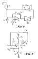
- Fig. 3 is a more detailed circuit diagram of the amplifier A.
- the transistor T r has its collector and emitter connected with power sources V cc and V ee through current sources CS1 and CS2 of the prior art, respectively.
- the emitter of the transistor T r is further connected through a bypass capacitor C o with the terminal g32 (at ground).
- the base of the transistor T r is the inverted input terminal of the amplifier A.
- a base-collector capacitor C1 and an output capacitor C2 are parasitic to the transistor T r .
- the output of the amplifier A is led out from the collector of the transistor T r through a buffer amplifier A1.
- the BT r is used at the first stage of the amplifier A
- the current measurement noise when a large impedance is to be measured is increased as seen from Equation (10) for a high DC bias current I c .
- the SR necessary for measurements with the high current and the high frequency is sufficiently short as may be seen from Equation (16) so that the automatic control loop is sufficiently destabilized to make the measurements impossible.
- the FET is improper for the DUT of a low impedance or for the measurements with high frequency and high current.
- both the BT r and the FET are used at the first stage of the amplifier A.
- the bias current value is fixed at a suitable compromising value so that the E n and the I n are not proper for the measurements of the DUT having a certain impedance.
- a compromise has to be made for the increase in noise for the measurement of the I x , and high-frequency and large-current measurements cannot be accomplished.
- an object of the present invention is to solve the above-specified problems by a circuit element measuring apparatus which executes high-frquency and large-current measurements precisely by controlling the amplifier A.
- a circuit element measuring apparatus for a device under test having one terminal and another terminal comprises a source of measurement voltage, means for detecting the measurement voltage, a zero detection amplifier, and a voltage-controlled source for drawing an electric current through the device to be measured in accordance with the output of the zero detection amplifier so as to drop the voltage of the other terminal of the device to be measured to zero.
- means are provided for changing the operation point of the zero detection amplifier in response to a measured condition.
- the operation point is the operating current of a first stage semiconductor element of the zero detection amplifier.
- the measuring condition is selected from a group consisting of the impedance of the device to be measured, feedback resistance of the zero detection amplifier, a measuring frequency, and a measuring current through the device.
- Fig. 1 is a schematic circuit diagram showing the circuit element measuring apparatus according to the prior art.
- Fig. 2 is a diagram for explaining the noise mode of Fig. 1.
- Fig. 3 is a schematic diagram showing one embodiment of the amplifier A of Fig. 1.
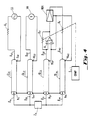
- Fig. 4 is a schematic circuit diagram showing the circuit element measuring apparatus according to one embodiment of the present invention.
- Fig. 4 is a schematic circuit diagram showing one embodiment of the present invention.
- the structure of the amplifier A used in Fig. 4 is shown in Fig. 3 where the parts serving the same functions are designated with common reference characters.
- Fig. 4 is different from Fig. 3 in that there is newly provided a control circuit block COMP.
- the prior art circuit element measuring apparatus of Fig. 1, according to the prior art is also equipped with a control not shown in Fig. 1.
- the function of setting the operation point of the amplifier A by setting the current I c in response to the control circuit COMP is not practiced by the prior art.
- the DC bias current I c of the first stage amplification element T r for the amplifier A is controlled in the following manner.
- the allowable range (I c1 , I c2 ) is given by Equation (10).
- I c1 , I c2 and I cmin are written into the following equations.
- I c1 0.025/2 x ⁇ R r //R f ⁇ / ⁇ Z x //R f ⁇ [A] (18)
- I c2 0.050 x h FE / ⁇ R r //R f ⁇ [A] (19)
- I cmin 2 ⁇ 2 ⁇ ⁇ fI x R f C t [A] (20) Equation (10) is written into the following form.
- the setting of the I c is determined to satisfy at least the Equation (16). In case, moreover, the I c can satisfy the Equation (10), it is set at that value. Otherwise, the I c is set at the minimum to satisfy the Equation (16) so that the value I n may be minimized.
- the I c may be set at about 1 mA from the Equation (12).
- the slew rate SR is increased by increasing either the collector voltage or the collector current.
- the object of the present invention is satisfied by raising the collector voltage with a high frequency. In this case, the power consumption of the transistor T r is increased.
- control circuit COMP may comprise a microprocessor capable of the aforesaid computations in response to the measuring conditions of the impedance (Z x ), the feedback resistance (R x ), a measuring frequency (f) or a measuring current I x for changing the operating point of the amplifier A, e.g., the current I c .
- the measurement accuracy and stability of the current I x to flow through the DUT can be improved.
- the accuracy and stability of the circuit element measurements are also improved. This result is achieved because the slew rate of the amplifier A sufficiently stabilizes the automatic control loop for measuring the value of I x and because the influence of noise on the amplifier A are reduced.
Landscapes
- Physics & Mathematics (AREA)
- General Physics & Mathematics (AREA)
- Measurement Of Resistance Or Impedance (AREA)
- Amplifiers (AREA)
Abstract
The circuit element being measured is connected to a signal source, a volt meter, a zero detection amplifier and a voltage controlled current source for drawing an electric current through the device to be measured in accordance with the output of the zero detection amplifier. Means are provided for changing the operating point of the zero detection amplifier in response to a measuring condition of the apparatus.
Description
- The present invention relates to a method and apparatus for high accuracy circuit element measurements by easily correcting changes, if any, in the measurement cables or range resistance.
- Demands for high-precision measurements of a circuit element are increasing annually. The apparatus for such measurements is exemplified by the "Multi-Frequency LCR meter 4274A or 4275A" which is commercially available from Yokogawa-Hewlett-Packard for use in four-terminal measurements. Fig. 1 is a schematic circuit diagram showing a circuit element measuring apparatus for four-terminal pair measurements according to the prior art.
- By means of four terminal lines CL₁, CL₂, CL₃, and CL₄ providing four terminal pairs, a circuit element to be measured (hereinafter referred to as a "DUT" or element Zx) is connected to a signal source SS, a volt meter VM, a range resistance Rr and a zero detection amplifier A which together form a measuring apparatus. The impedance value of the element Zx shall also be referred to as Zx.
- The lines CL₁, CL₂, CL₃ and CL₄ are generally made of coaxial cables although not limited thereto, and their outer conductor terminals g₁₁, g₂₁, g₃₁ and g₄₁ at one end thereof are connected to one another and held at the same potential. The terminals ℓ₁₁ and ℓ₂₁ of the center conductor of the lines CL₁ and CL₂ at the same end thereof are connected to one terminal of the element Zx. The terminals ℓ₃₁ and ℓ₄₁ of CL₃ and CL₄ are connected to the other terminal of the element Zx. The terminals of the center conductors of the lines CL₁, CL₂, CL₃ and CL₄ and the outer conductor at the opposite end (i.e. at the side on the meter) are respectively designated as ℓ₁₂, g₁₂, ℓ₂₂, g₂₂, ℓ₃₂, g₃₂, ℓ₄₂ and g₄₂.
- Between the terminals 1₁₂ and g₁₂, the signal source SS and a signal source resistance Rs are connected in series. The volt meter VM is connected between the terminals ℓ₂₂ and g₂₂. The terminals ℓ₃₂ and g₃₂ are respectively connected to the inverted input terminal and non-inverted input terminal of the zero detection amplifier A. The feedback resistance Rf is connected between the inverted input terminal and the output terminal of the zero detection amplifier A. The output of the zero detection amplifier A is introduced into a narrow-band amplification/phase compensation amplifier NBA. The output of the NBA is applied through the range resistance Rr to the terminal ℓ₄₂. The NBA is similar to that used in the aforementioned meters 4274A and 4275A. The range resistance Rr is placed between the terminal 1₄₂ and the NBA output, and the terminals g₄₂ and g₃₂ are also connected.
- In the circuit of Fig. 1, an automatic control is performed on the voltage between the terminals ℓ₃₂ and g₃₂, i.e., controlled such that the current flow through the terminal ℓ₃₂ may be substantially zero. As a result, a voltage Vx to be applied to the element Zx is obtained as the indication of the volt meter VM. Moreover, a current Ix to flow through the element Zx is obtained as an indication of the range resistance Rr. Since a complex voltage and a complex current are measured at the volt meter VM and the range resistance Rr with reference to the detected output of the signal source SS, the value Zx is determined in a complex value in accordance with the following equation:

wherein Vi is equal to the voltage generated across the Rr and is expressed as

- The method of measuring the complex voltage or current is well known in the art and is used together with the overall operations of the meter in the aforementioned 4274A or 4275A. The calibrations are carried out by the known method of replacing the measured element with a "short" or "open" or by using a known third impedance.
- It will be understood that the range resistance Rr is selected to have a magnitude close to that of the Zx. This provides the advantage of a uniform dynamic range for succeeding volt meters by making the magnitudes of the Vx and Vi same.
- It will also be understood that the stabilization of the automatic control loop composed of the line CL₃, the zero detection amplifier A, the NBA, the range resistance Rr and the line CL₄ can be made excellent by selecting a sufficiently small value of the feedback resistance Rf.
- Reference will now be made to Fig. 2 wherein a noise model of the automatic control loop of Fig. 1 is shown so as to provide an understanding of the problem of noise in the prior art thus far described. Referring to Fig. 2, reference characters E₁, and E₂ designate the thermal noise of the resistors Rr and Rf respectively; and characters En and In designate an equivalent input noise voltage and an equivalent input noise current of the zero detection amplifier A respectively. These four noise sources are deemed to be random and therefore have no correlation among themselves. Moreover, the individual noise sources are considered as white noise sources, as will be expressed by the following theoretical equations.


wherein: - k
- is Boltzmann's constant
= 1.38 x 10⁻²³ [W s/K]; - T
- is absolute temperature [K]; and
- f
- is observation band width [Hz].
- In case the amplification element at the first stage of the zero detection amplifier A is a bipolar transistor (BTr),


wherein: - re
- is kT/(q·Ic),
kT/q = 25 mV (T = 300 K); - q
- is electron charge = 6.02 x 10⁻¹⁹ [C];
- Ic
- is collector current [A]; and
- hFE
- is short-circuit current gain.
- In case the first-stage amplification element of the amplifier A is a field effect transistor (i.e., FET),

wherein gm is mutual conductance [S] of the FET. The value In can usually be ignored. - If a volt meter VI is one for measuring the voltage Vi, the summation Vn of the noise measured by the volt meter VI is deduced in the following form because the individual noise sources have no correlation:

wherein, x//y is the parallel connection xy/(x+y). From Equation (6), it is found that the Vn² increases more the smaller Rf is as compared with Rr in the case of Rr<Zx. It is, therefore, advisable that the Rf should not be less than the Rr. - In order that an increase of the summation Vn because of the noises En and In of the amplifier A may not be more than 3 dB, the two terms of the latter half of the Equation (6) must not be larger than the two terms of the former half:

- Since the values En and In of the Equation (7) provide no simultaneous major causes of noise, the following necessary conditions are obtained by setting In = 0 or En = 0:


- Although FETs have a sufficiently small In but few FETs have a smaller En than 2nV/ (Hz) and an FET is less suitable than the BTr (i.e., bipolar transistor) for the measurement of the DUT of a lower impedance because of higher DC bias current is needed.
- By using the relations among Equations (1) to (4), (8) and (9), the bias conditions for the BTr may be determined as follows:

- If a DUT having Zx = 50Ω, for example, is to be measured, a suitable setting is Rr = Rf = 50Ω for reasons previously described. If a BTr having hEF = 100 is used at the first stage of the amplifier A, the following relations are obtained from Equation (10) so that the noises of the amplifier A may not increase the Vn to 3 dB or more.

Likewise, the following relations are obtained if a BTr having hFE = 100 is used at the first stage of the amplifier A for the measurements of Zx = 10 K and Rr = Rf - 10KΩ:

- As can be found from Equations (11) and (12), the optimum value for the bias current Ic of the amplification element at the first stage of the amplifier A is different for the case, in which a DUT of a low impedance is to be measured, and for the case in which a DUT of a high impedance is to be measured. In the prior art, the bias current Ic uses a fixed value but not the proper value. Next, the slew rate of the amplifier A is to be considered. In Fig. 1, it is necessary for the convergence of the aforementioned automatic control loop that the input voltage of the amplifier A be sufficiently close to zero. When the DUT is to be measured with a high measurement frequency and/or a large measurement current, the change of the Ix per unit time is enlarged. If the slew rate of the amplifier A becomes smaller, the amplifier A cannot absorb more than a portion of the Ix. Then, the automatic control loop may perform in a nonlinear fashion and fail to converge.
- The output voltage Vo of the amplifier A can be expressed as the following function of time t.

wherein: - Ix
- is measured current (rms);
- f
- is measurement frequency.
- When the output voltage Vo is differentiated with time,

- The slew rate of the amplifier A has to be larger than the maximum (√
2) ·2Πf·Ix·Rf. Fig. 3 is a more detailed circuit diagram of the amplifier A. In Fig. 3, the transistor Tr has its collector and emitter connected with power sources Vcc and Vee through current sources CS₁ and CS₂ of the prior art, respectively. The emitter of the transistor Tr is further connected through a bypass capacitor Co with the terminal g₃₂ (at ground). The base of the transistor Tr is the inverted input terminal of the amplifier A. A base-collector capacitor C₁ and an output capacitor C₂ are parasitic to the transistor Tr. The output of the amplifier A is led out from the collector of the transistor Tr through a buffer amplifier A₁. The slew rate of the circuit of Fig. 3 is determined by the transistor Tr and the peripheral circuit, as follows.

Wherein: - SR
- is the slew rate;
- Ct
- = C₁ + C₂;
- Ic
- is the DC bias current to flow through the first stage amplification elements.
- Our experiments have revealed it difficult to improve the SR drastically even with another structure of the amplifier A. In order that the automatic control loop may properly operate, it is necessary that Equation (15) > Equation (14).

- In the case of Zx = Rr = Rf = 50Ω, Ix = 50 mA, f = 50 MHz and Ct = 20 pF, for example, the following relation has to hold.

- In order to make possible the measurement of a high frequency and a high current, as has been described hereinbefore, it is necessary to minimize the Rf and to sufficiently maximize the DC bias current Ic flowing through the first stage of the amplifier A. In case an FET is used at the first stage of the amplifier A, the DUT cannot be properly measured in the high frequency and with the large current because the Ic is limited by the IDSS of the FET. If, on the other hand, the Ic is increased, the noise In is augmented irrespective of the frequency.
- The description thus far made could be summarized in the following form. In case that the BTr is used at the first stage of the amplifier A, the current measurement noise when a large impedance is to be measured is increased as seen from Equation (10) for a high DC bias current Ic. For a low bias current Ic, on the other hand, the SR necessary for measurements with the high current and the high frequency is sufficiently short as may be seen from Equation (16) so that the automatic control loop is sufficiently destabilized to make the measurements impossible. Moreover, the FET is improper for the DUT of a low impedance or for the measurements with high frequency and high current.
- In the case of the products of the prior art, both the BTr and the FET are used at the first stage of the amplifier A. However, the bias current value is fixed at a suitable compromising value so that the En and the In are not proper for the measurements of the DUT having a certain impedance. Thus, a compromise has to be made for the increase in noise for the measurement of the Ix, and high-frequency and large-current measurements cannot be accomplished.
- It is, therefore, an object of the present invention is to solve the above-specified problems by a circuit element measuring apparatus which executes high-frquency and large-current measurements precisely by controlling the amplifier A.
- In accordance with the foregoing and other objects of the invention, a method and apparatus are provided wherein a circuit element measuring apparatus for a device under test having one terminal and another terminal comprises a source of measurement voltage, means for detecting the measurement voltage, a zero detection amplifier, and a voltage-controlled source for drawing an electric current through the device to be measured in accordance with the output of the zero detection amplifier so as to drop the voltage of the other terminal of the device to be measured to zero.
- In accordance with this invention, means are provided for changing the operation point of the zero detection amplifier in response to a measured condition. Preferably, the operation point is the operating current of a first stage semiconductor element of the zero detection amplifier. The measuring condition is selected from a group consisting of the impedance of the device to be measured, feedback resistance of the zero detection amplifier, a measuring frequency, and a measuring current through the device.
- Fig. 1 is a schematic circuit diagram showing the circuit element measuring apparatus according to the prior art.
- Fig. 2 is a diagram for explaining the noise mode of Fig. 1.
- Fig. 3 is a schematic diagram showing one embodiment of the amplifier A of Fig. 1.
- Fig. 4 is a schematic circuit diagram showing the circuit element measuring apparatus according to one embodiment of the present invention.
- Fig. 4 is a schematic circuit diagram showing one embodiment of the present invention. The structure of the amplifier A used in Fig. 4 is shown in Fig. 3 where the parts serving the same functions are designated with common reference characters. Fig. 4 is different from Fig. 3 in that there is newly provided a control circuit block COMP. Note, however, that the prior art circuit element measuring apparatus of Fig. 1, according to the prior art is also equipped with a control not shown in Fig. 1. However, the function of setting the operation point of the amplifier A by setting the current Ic in response to the control circuit COMP is not practiced by the prior art.
- In the embodiment of the present invention, the DC bias current Ic of the first stage amplification element Tr for the amplifier A is controlled in the following manner. First of all, the range resistance Rr is determined if the impedance Zx of the DUT, the measurement current Ix and the measurement frequency f are given. Since the voltage to be generated in the range resistance Rr is limited to the maximum Vmax, the resistance Rr selects a value smaller than Vmax/Ix = Rrmax and near Rrmax. The resistance Rf selected is near the selected value of the Rr. The allowable range (Ic1, Ic2) is given by Equation (10).
- Next, with the known capacity Ct of the transistor Tr, the minimum Icmin of the allowable Ic is given from Equation (16).
- The values Ic1, Ic2 and Icmin are written into the following equations.


Equation (10) is written into the following form.

- The setting of the Ic is determined to satisfy at least the Equation (16). In case, moreover, the Ic can satisfy the Equation (10), it is set at that value. Otherwise, the Ic is set at the minimum to satisfy the Equation (16) so that the value In may be minimized.
- In case a DUT of Zx = 10 KΩ, for example, is to be measured with a low frequency, the Ic may be set at about 1 mA from the Equation (12). In case, on the other hand, a DUT of Zx = 50Ω is to be measured for Ix = 50 mA and F = 50 MHz, the measurements can be performed for Ic = 22 mA from Equation (17) without deterioration of the stability of the automatic control loop.
- In the embodiment thus far described, no special consideration is taken into the sections of the Rr, Rf, Ix and f, which can be economically limited to discrete values.
- In case the value Zx is unknown, on the other hand, there can be easily conceived convenient means for determining the value Ic by advancing the computations assuming that the value Zx be equal to the value Rr. It is also conceivable to reduce the values C₁ and C₂ (by raising the collector voltage) so as to increase the value SR.
- Since the operation point of the transistor Tr is determined by the collector voltage and the collector current, the slew rate SR is increased by increasing either the collector voltage or the collector current. Thus, the object of the present invention is satisfied by raising the collector voltage with a high frequency. In this case, the power consumption of the transistor Tr is increased.
- It will be appreciated that the control circuit COMP may comprise a microprocessor capable of the aforesaid computations in response to the measuring conditions of the impedance (Zx), the feedback resistance (Rx), a measuring frequency (f) or a measuring current Ix for changing the operating point of the amplifier A, e.g., the current Ic.
- As has been described in detail hereinbefore, according to the embodiment of the present invention, the measurement accuracy and stability of the current Ix to flow through the DUT can be improved. As a result, the accuracy and stability of the circuit element measurements are also improved. This result is achieved because the slew rate of the amplifier A sufficiently stabilizes the automatic control loop for measuring the value of Ix and because the influence of noise on the amplifier A are reduced.
Claims (13)
- A circuit element measuring apparatus for a device having one terminal and another terminal, said apparatus comprising:
a signal source;
a first line connecting said one terminal to said signal source for applying a voltage to said terminals;
a volt meter;
a second line connecting said one terminal to said volt meter for measuring said voltage applied to said one terminal;
a zero detection amplifier;
a third line connecting the other terminal of said element to said zero detection amplifier for detecting the voltage of said other terminal;
a voltage controlled source;
a fourth line for connecting said other terminal with said voltage control source for drawing an electric current flowing through said element in accordance with the output of said zero detection amplifier so as to drop the voltage of said other terminal to zero;
and means for changing the operation point of the zero detection amplifier in accordance with a measuring condition of said measuring apparatus. - The circuit element measuring apparatus of claim 1 wherein said measuring condition includes the impedance of the element to be measured.
- The circuit element measuring apparatus of claim 1 wherein said measuring condition is a feedback resistance of said zero detection amplifier.
- The circuit element measuring apparatus of claim 1 wherein said measuring condition includes a measuring frequency.
- The circuit element measuring apparatus of claim 1 wherein said measuring condition includes the measuring current through the device.
- The circuit element measuring apparatus of claim 1 wherein said measuring condition is selected from a group consisting of the impedance of the device to be measured, a feedback resistance of the zero detection amplifier, a measuring frequency and a measuring current through the DUT.
- The circuit element measuring apparatus of claim 1 wherein said zero detection amplifier includes a first stage having a semiconductor element and the means for changing the operation point changes the operation current through said semiconductor element.
- A circuit element measuring apparatus for a device under test having one terminal and another terminal, said apparatus comprising:
means for applying a measurement voltage to one terminal of said device;
means for detecting the measurement voltage applied to said one terminal of said device;
zero detection amplifier means coupled to the other terminal of said device for detecting the voltage at said other terminals;
a voltage controlled current source for drawing an electric current through said element in accordance with the output of said zero detection amplifier to drop the voltage of said other terminal to zero;
shielded line means coupling said device to said means for applying a measurement voltage, said means for detecting the measurement voltage, said zero detection amplifier, and said voltage-controlled current source; and
means for changing the operation point of said zero detection amplifier in response to a measuring condition of said apparatus. - The circuit element measuring apparatus of claim 8 wherein said measuring condition is selected from a group consisting of the impedance of said element to be measured, the feedback resistance of the zero detection amplifier, a measuring frequency and a measuring current through the element to be measured.
- The circuit element measuring apparatus of claim 8 wherein said zero detection amplifier comprises a first stage having a semiconductor element and said means for changing the operation point of said zero detection amplifier comprises means for changing the operating current of said first stage semiconductor element.
- A method of operating a circuit device measuring apparatus for a device under test having one terminal and another terminal comprising a source of measurement voltage, means for detecting the measurement voltage, a zero detection amplifier, a voltage controlled current source for drawing an electric current through said device in accordance with the output of said zero detection amplifier to drop the voltage of said other terminal to zero and shielded lines coupled thereto, said method comprising the following steps:
applying a measurement voltage from said source to said one terminal;
detecting the measurement voltage applied to said one terminal by said means for detecting;
detecting the voltage at said other terminal with said zero detection amplifier; and
means for changing the operating point of said zero detection amplifier in response to a measuring condition of the apparatus. - The method of claim 11 wherein said zero detection amplifier includes a first stage semiconductor element and the step of changing the operating point of said zero detection amplifier includes changing the operating current of said first stage semiconductor element.
- The method of claim 11 wherein the operating point is changed in accordance with a measuring condition selected from the group consisting of the impedance of the device to be measured, a feedback resistance of the zero detection amplifier, a measuring frequency and a measuring current through the device to be measured.
Applications Claiming Priority (2)
| Application Number | Priority Date | Filing Date | Title |
|---|---|---|---|
| JP2049052A JP2960095B2 (en) | 1990-02-27 | 1990-02-27 | Circuit element measuring device |
| JP49052/90 | 1990-02-27 |
Publications (2)
| Publication Number | Publication Date |
|---|---|
| EP0444816A2 true EP0444816A2 (en) | 1991-09-04 |
| EP0444816A3 EP0444816A3 (en) | 1992-05-13 |
Family
ID=12820312
Family Applications (1)
| Application Number | Title | Priority Date | Filing Date |
|---|---|---|---|
| EP19910301343 Withdrawn EP0444816A3 (en) | 1990-02-27 | 1991-02-20 | Circuit element measuring method and apparatus |
Country Status (4)
| Country | Link |
|---|---|
| US (1) | US5086278A (en) |
| EP (1) | EP0444816A3 (en) |
| JP (1) | JP2960095B2 (en) |
| CA (1) | CA2036263A1 (en) |
Families Citing this family (3)
| Publication number | Priority date | Publication date | Assignee | Title |
|---|---|---|---|---|
| JP3329555B2 (en) * | 1993-12-28 | 2002-09-30 | アジレント・テクノロジー株式会社 | Impedance meter |
| US20080229506A1 (en) * | 2007-03-19 | 2008-09-25 | Saman Natalie T | Diaper changing article |
| US8896331B2 (en) * | 2008-02-01 | 2014-11-25 | Keithley Instruments, Inc. | Impedance measuring instrument |
Family Cites Families (7)
| Publication number | Priority date | Publication date | Assignee | Title |
|---|---|---|---|---|
| US4241316A (en) * | 1979-01-18 | 1980-12-23 | Lawrence Kavanau | Field effect transconductance amplifiers |
| US4264871A (en) * | 1979-04-16 | 1981-04-28 | Hughes Aircraft Company | Low noise amplifiers |
| US4577160A (en) * | 1983-01-03 | 1986-03-18 | Robert H. Rines | Method of and apparatus for low noise current amplification |
| JPS6158307A (en) * | 1984-08-30 | 1986-03-25 | Nec Ic Microcomput Syst Ltd | Gain variable amplifier |
| JPH026268U (en) * | 1988-06-28 | 1990-01-16 | ||
| JP2698615B2 (en) * | 1988-07-05 | 1998-01-19 | 日本ヒューレット・パッカード株式会社 | Circuit element measuring device |
| US4905308A (en) * | 1989-04-05 | 1990-02-27 | Cascade Microtech, Inc. | Noise parameter determination method |
-
1990
- 1990-02-27 JP JP2049052A patent/JP2960095B2/en not_active Expired - Fee Related
-
1991
- 1991-02-13 CA CA002036263A patent/CA2036263A1/en not_active Abandoned
- 1991-02-20 EP EP19910301343 patent/EP0444816A3/en not_active Withdrawn
- 1991-02-22 US US07/659,853 patent/US5086278A/en not_active Expired - Lifetime
Also Published As
| Publication number | Publication date |
|---|---|
| JPH03249570A (en) | 1991-11-07 |
| CA2036263A1 (en) | 1991-08-28 |
| JP2960095B2 (en) | 1999-10-06 |
| EP0444816A3 (en) | 1992-05-13 |
| US5086278A (en) | 1992-02-04 |
Similar Documents
| Publication | Publication Date | Title |
|---|---|---|
| US5970429A (en) | Method and apparatus for measuring electrical noise in devices | |
| US6856129B2 (en) | Current probe device having an integrated amplifier | |
| EP0320265B1 (en) | Wide dynamic range radio-frequency power sensor | |
| US4647848A (en) | Broadband RF power detector using FET | |
| US6642741B2 (en) | Electronically adjustable integrated circuit input/output termination method and apparatus | |
| US3048776A (en) | Resistivity measuring circuit | |
| Cutkosky | An ac resistance thermometer bridge | |
| US6822433B1 (en) | Gain and phase detector having dual logarithmic amplifiers | |
| US5448173A (en) | Triple-probe plasma measuring apparatus for correcting space potential errors | |
| US3227953A (en) | Bridge apparatus for determining the input resistance and beta figure for an in-circuit transistor | |
| EP0444816A2 (en) | Circuit element measuring method and apparatus | |
| EP3101435B1 (en) | Power detection | |
| CA1310368C (en) | Circuit element measuring apparatus | |
| US5732332A (en) | Transmitter having temperature-compensated detector | |
| US6608492B1 (en) | AC impedance bridge | |
| US20030173984A1 (en) | Current-comparator-based four-terminal resistance bridge for power frequencies | |
| JP2698615B2 (en) | Circuit element measuring device | |
| US4039945A (en) | Device for measuring and checking parameters of electric circuit elements | |
| EP0874245A1 (en) | Method and apparatus for determining the noise characteristics of an electrical device | |
| Baechtold et al. | Noise in microwave transistors | |
| US2897448A (en) | Circuit for measuring alpha of transistors | |
| JPS5910506B2 (en) | electronic measuring instruments | |
| JPH02300670A (en) | Inductance measuring instrument | |
| CN222994565U (en) | Radio frequency probe circuit | |
| Zawels | A wide-band bridge yielding directly the device parameters of junction transistors |
Legal Events
| Date | Code | Title | Description |
|---|---|---|---|
| PUAI | Public reference made under article 153(3) epc to a published international application that has entered the european phase |
Free format text: ORIGINAL CODE: 0009012 |
|
| AK | Designated contracting states |
Kind code of ref document: A2 Designated state(s): DE FR GB |
|
| PUAL | Search report despatched |
Free format text: ORIGINAL CODE: 0009013 |
|
| AK | Designated contracting states |
Kind code of ref document: A3 Designated state(s): DE FR GB |
|
| STAA | Information on the status of an ep patent application or granted ep patent |
Free format text: STATUS: THE APPLICATION IS DEEMED TO BE WITHDRAWN |
|
| 18D | Application deemed to be withdrawn |
Effective date: 19930129 |