EP0443660B1 - Magnetowiderstand - Google Patents
Magnetowiderstand Download PDFInfo
- Publication number
- EP0443660B1 EP0443660B1 EP91200268A EP91200268A EP0443660B1 EP 0443660 B1 EP0443660 B1 EP 0443660B1 EP 91200268 A EP91200268 A EP 91200268A EP 91200268 A EP91200268 A EP 91200268A EP 0443660 B1 EP0443660 B1 EP 0443660B1
- Authority
- EP
- European Patent Office
- Prior art keywords
- openings
- semi
- film
- paths
- magnetoresistor
- Prior art date
- Legal status (The legal status is an assumption and is not a legal conclusion. Google has not performed a legal analysis and makes no representation as to the accuracy of the status listed.)
- Expired - Lifetime
Links
- 239000010408 film Substances 0.000 claims description 40
- 239000004065 semiconductor Substances 0.000 claims description 36
- 239000000463 material Substances 0.000 claims description 10
- 239000010409 thin film Substances 0.000 claims description 7
- 239000000758 substrate Substances 0.000 description 6
- JBRZTFJDHDCESZ-UHFFFAOYSA-N AsGa Chemical compound [As]#[Ga] JBRZTFJDHDCESZ-UHFFFAOYSA-N 0.000 description 2
- 229910001218 Gallium arsenide Inorganic materials 0.000 description 2
- RPQDHPTXJYYUPQ-UHFFFAOYSA-N indium arsenide Chemical compound [In]#[As] RPQDHPTXJYYUPQ-UHFFFAOYSA-N 0.000 description 2
- 230000037230 mobility Effects 0.000 description 2
- 229910000530 Gallium indium arsenide Inorganic materials 0.000 description 1
- 229910000673 Indium arsenide Inorganic materials 0.000 description 1
- 239000002800 charge carrier Substances 0.000 description 1
- 238000005229 chemical vapour deposition Methods 0.000 description 1
- 230000001419 dependent effect Effects 0.000 description 1
- 238000000151 deposition Methods 0.000 description 1
- 238000000609 electron-beam lithography Methods 0.000 description 1
- 230000008020 evaporation Effects 0.000 description 1
- 238000001704 evaporation Methods 0.000 description 1
- WPYVAWXEWQSOGY-UHFFFAOYSA-N indium antimonide Chemical compound [Sb]#[In] WPYVAWXEWQSOGY-UHFFFAOYSA-N 0.000 description 1
- 239000011810 insulating material Substances 0.000 description 1
- 229910052751 metal Inorganic materials 0.000 description 1
- 239000002184 metal Substances 0.000 description 1
- 238000000034 method Methods 0.000 description 1
- 238000004544 sputter deposition Methods 0.000 description 1
Images
Classifications
-
- H—ELECTRICITY
- H10—SEMICONDUCTOR DEVICES; ELECTRIC SOLID-STATE DEVICES NOT OTHERWISE PROVIDED FOR
- H10N—ELECTRIC SOLID-STATE DEVICES NOT OTHERWISE PROVIDED FOR
- H10N50/00—Galvanomagnetic devices
- H10N50/10—Magnetoresistive devices
Definitions
- the present invention relates to a thin film magnetoresistor as specified in the preamble of claim 1, for example as disclosed in SU-A-920596.
- Magnetoresistors are resistors whose resistance is varied by applying a magnetic field across the resistor. Magnetoresistors can be used, in conjunction with a permanent magnet, to sense the distance between the magnet and the magnetoresistors. This leads to their potential application in position sensing devices, such as are used in the automotive industry.
- One class of these devices known as magnetodiodes, operates on the basis of selective re-combination of electrons and holes.
- the other class operates on the deflection of the current paths in a rectangular or circular resistor.
- the performance of the first class of devices depends strongly on the electron-hole re-combination rate, and the performance of the second class of devices depends on the carrier mobilities.
- a magnetoresistor according to the present invention is chacterised by the features specified in the characterising portion of claim 1.
- the present invention is directed to a thin film magnetoresistor in which the path of the resistance material is such that, when the device is subjected to a magnetic field, electrons flow in substantially a circular path so as to increase the resistance of the device.
- the magnetoresistor comprises a thin film of a degenerately-doped semi-conductor material having a pair of conductive contacts at opposite ends of the film.
- the film is in the form of a series of paths which extend at least partially in a substantially circular pattern.
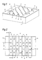
- the magnetoresistor 10 comprises a substrate 12 of an insulating material, such as iron-doped gallium arsenide, having a thin film 14 of a degenerately-doped semi-conductor material, such as indium arsenide or indium antimonide, on a surface 16 thereof.
- the semi-conductor film 14, which is the active layer of the magnetoresistor, is of a thickness of no greater than about 5 micrometres, and preferably has a thickness no greater than about 3 micrometres.
- the semi-conductor film 14 is substantially rectangular, and separate conductive contacts 18 and 20 are on the substrate surface 16 at opposite edges of the semi-conductor film 14. The contacts 18 and 20 are in ohmic contact with the semi-conductor film 14.
- the semi-conductor film 14 has a plurality of openings 22 therethrough in the form of circular holes which are arranged in spaced parallel rows extending across the film 14 parallel to the contacts 18 and 20.
- the holes 22 in alternate rows are arranged between the holes 22 in the adjacent rows.
- the spacing between the holes 22, i.e., the width of the paths 24 and 26, should be no greater than the mean free path of electrons in the semi-conductor film 14.
- the holes 22 should have a radius such that the perimeter (circumference) of the hole is no greater than the mean free path of electrons in semi-conductor material of film 14.
- the mean free path is about 300 nanometres (3000 Angstroms).
- each hole 22 acts as a minuscule cyclotron, and electrons flow along the paths 24 and 26 around the holes 22 as indicated by the arrows 28. The electrons so flow until they either re-combine or scatter. This results in an increase in the resistance of the magnetoresistor 10.
- the field at which this occurs is only a function of the geometry. This is so because the electron effective mass, and its Fermi velocity are parameters which are quite temperature-independent in degenerate semi-conductors. Thus, the magnetoresistor 10 has a high resistance and a low temperature coefficient.
- the magnetoresistor 30 comprises a thin film 32 of degenerated semi-conductor material on the surface of an insulating substrate 34, and conductive contacts 36 and 38 on the substrate at opposite ends of the semi-conductor film 32.
- the semi-conductor film 32 comprises a plurality of spaced, parallel first paths 40 extending parallel to the contacts 36 and 38, and a plurality of spaced second paths 42 extending between the first paths 40 substantially perpendicular to the contacts 36 and 38.
- the second paths 42 between two adjacent first paths 40 are not aligned with the second paths 42 between the next adjacent pairs of first paths 40 so as to form openings 43 which are arranged in a substantially staggered brick-work pattern.
- the spacing N between adjacent first paths 40 is no greater than one-third of the mean free path of electrons in the semi-conductor film 32, and is preferably smaller than one-third of the mean free path.
- the spacing 2N between adjacent second paths 42 is about twice the spacing between adjacent first paths 40.
- the thickness of the paths 40 and 42 is about 2/5N.
- a voltage applied between the contacts 36 and 38 causes a flow of current along the paths 40 and 42.
- a magnetic field is applied perpendicular to the surface of the semi-conductor film 32, at each intersection of a first path 40 and a second path 42, the charge carriers are preferentially steered in one direction in a substantially circular path around a corner or opening 43 by the Lorentz force as indicated by the arrows 44. This blocks the flow of electrons along the semi-conductor film 32 so as to achieve an increase in the resistance.
- the magnetic field applied to the magnetoresistor 30 results in an increase in the magnetoresistance.
- the magnetoresistor 30 also has a low temperature coefficient.
- the magnetoresistors 10 and 30 may be made by depositing a film of the semi-conductor material on the surface of a substrate using any suitable chemical vapor-deposition process for the particular material used. Metal contacts are then deposited on the substrate surface at the ends of the semi-conductor film either by evaporation in a vacuum or by sputtering.
- the holes 22 in the semi-conductor film of the magnetoresistor 10 and the openings between the paths 40 and 42 in the semi-conductor film of the magnetoresistor 30 are formed by electron-beam lithography.
- a magnetoresistor in which the paths of the semi-conductor film are designed so that, when a magnetic field is applied to the semi-conductor film, the electrons will flow in a circular path and thereby increase the resistance of the magnetoresistor.
- the factors which affect this increase in resistance are temperature-independent so that the temperature coefficient of the magnetoresistor is low.
Landscapes
- Hall/Mr Elements (AREA)
- Thermistors And Varistors (AREA)
Claims (5)
- Ein Magnetoresistor (10; 30) mit: einem dünnen Film (14; 32) eines Halbleitermaterials und einem Paar von leitenden Kontakten (18, 20; 36, 38) an entgegengesetzten Enden des Films (14; 32), wobei der Film Öffnungen (22; 43) aufweist, die dort hindurch derart gebildet sind, daß, wenn ein Magnetfeld senkrecht zu dem Halbleiterfilm (14; 32) angelegt wird, der elektrische Widerstandswert zwischen den leitenden Kontakten (18, 20; 36, 38) zunimmt,
dadurch gekennzeichnet,
daß das Halbleitermaterial ein degenerativ dotiertes Halbleitermaterial ist, welches von einer Dicke nicht größer als 5 Mikrometer ist und welches eine gegebene mittlere freie Weglänge von Elektronen in dem dünnen Film (14; 32) vorsieht; die Öffnungen (22; 43) in dem Halbleiterfilm (14; 32) parallele Reihen von gleichförmig gestalteten Öffnungen (22; 43) darin bilden, wobei die Öffnungen Abmessungen aufweisen, die klein genug sind, um einen Öffnungsumfang zu schaffen, der nicht größer als die mittlere freie Weglänge der Elektronen in dem Halbleiterfilm (14; 32) ist; die Öffnungen (22; 43) voneinander um einen vorbestimmten Abstand beabstandet ist, der nicht größer als die mittlere freie Weglänge der Elektronen in dem Halbleiterfilm (14; 32) sind; die Reihen der Öffnungen (22; 43) lateral beabstandete Pfade (26; 42) in dem Halbleiterfilm (14; 32) vorsehen, welche im wesentlichen senkrecht zu den leitenden Kontakten (18, 20; 36, 38) liegen; die Reihen der Öffnungen (22; 43) longitudinal beabstandete Wege (24; 40) in dem halbleitenden Film (14; 32) vorsehen, welche im wesentlichen parallel zu den leitenden Kontakten (18, 20; 36, 38) liegen; die beabstandeten Pfade jede eine Breite nicht größer die mittlere freie Weglänge der Elektronen in dem Halbleiterfilm (14; 32) aufweisen; und die parallelen und senkrechten Pfade (24, 26; 40, 42) sich miteinander an Orten benachbart den Öffnungen (22; 43) schneiden, um im wesentlichen ringförmige Wege um die Öffnungen (22; 43) derart zu schaffen, daß, wenn das Magnetfeld senkrecht zu dem Halbleiterfilm (14; 32) angelegt wird, Elektronen, die durch den Halbleiterfilm (14; 32) zwischen den leitenden Kontakten (18, 20; 36, 38) fließen, dazu veranlaßt werden, in im wesentlichen ringförmigen Wegen (28; 44) um zumindest einige der Öffnungen (22; 43) zu fließen, um dadurch den elektrischen Widerstandswert zwischen den leitenden Kontakten (18, 20; 36, 38) zu erhöhen. - Ein Magnetoresistor (10; 30) nach Anspruch 1, in welchem die Öffnungen (22; 43) in Reihen im wesentlichen parallel zu den leitenden Kontakten (18, 20; 36, 38) angeordnet sind, wobei die Öffnungen (22; 43) in jeder Reihe lateral von den Öffnungen (22; 43) in den benachbarten Reihen versetzt und dazwischen beabstandet sind.
- Ein Magnetoresistor (10) nach Anspruch 1 oder 2, in welchem die Öffnungen kreisförmige Löcher (22) sind.
- Ein Magnetoresistor (30) nach Anspruch 1 oder 2, in welchem die Öffnungen (43) viereckig in der Form sind, wobei jede viereckige Öffnung (43) ein Ausmaß N in der Richtung senkrecht zu den Kontakten (36, 38) aufweist, das nicht größer als ein Drittel der mittleren freien Weglänge der Elektronen durch den Film (32) ist, und eine Ausdehnung parallel zu den Kontakten (36, 38) aufweist, welche 2N äquivalent ist.
- Ein Magnetoresistor (30) nach Anspruch 4, in welchem die Wege (40, 42) des Films (32) beabstandete parallele erste Teile (40), die sich parallel zu den Kontakten (36, 38) erstrecken, und beabstandete parallele zweite Teile (42) aufweisen, die sich zwischen dem ersten Teil (40) erstrecken, um die rechteckigen Öffnungen (43) zu bilden.
Applications Claiming Priority (2)
| Application Number | Priority Date | Filing Date | Title |
|---|---|---|---|
| US07/483,689 US5038131A (en) | 1990-02-23 | 1990-02-23 | Magnetoresistor |
| US483689 | 1990-02-23 |
Publications (2)
| Publication Number | Publication Date |
|---|---|
| EP0443660A1 EP0443660A1 (de) | 1991-08-28 |
| EP0443660B1 true EP0443660B1 (de) | 1994-11-30 |
Family
ID=23921123
Family Applications (1)
| Application Number | Title | Priority Date | Filing Date |
|---|---|---|---|
| EP91200268A Expired - Lifetime EP0443660B1 (de) | 1990-02-23 | 1991-02-08 | Magnetowiderstand |
Country Status (3)
| Country | Link |
|---|---|
| US (1) | US5038131A (de) |
| EP (1) | EP0443660B1 (de) |
| DE (1) | DE69105294T2 (de) |
Families Citing this family (7)
| Publication number | Priority date | Publication date | Assignee | Title |
|---|---|---|---|---|
| US5883564A (en) * | 1994-04-18 | 1999-03-16 | General Motors Corporation | Magnetic field sensor having high mobility thin indium antimonide active layer on thin aluminum indium antimonide buffer layer |
| EP0678925A1 (de) * | 1994-04-18 | 1995-10-25 | General Motors Corporation | Magnetfeldsensor |
| US5491461A (en) * | 1994-05-09 | 1996-02-13 | General Motors Corporation | Magnetic field sensor on elemental semiconductor substrate with electric field reduction means |
| US5561079A (en) * | 1994-12-16 | 1996-10-01 | General Motors Corporation | Stalagraphy |
| US6510031B1 (en) * | 1995-03-31 | 2003-01-21 | International Business Machines Corporation | Magnetoresistive sensor with magnetostatic coupling to obtain opposite alignment of magnetic regions |
| US6075437A (en) * | 1998-03-09 | 2000-06-13 | General Motors Corporation | In-plane magnetoresistance bridge |
| JP3651433B2 (ja) * | 2001-09-28 | 2005-05-25 | 株式会社村田製作所 | 磁気センサ |
Family Cites Families (10)
| Publication number | Priority date | Publication date | Assignee | Title |
|---|---|---|---|---|
| GB1309785A (en) * | 1969-05-16 | 1973-03-14 | Exxon Research Engineering Co | Promotor for acid gas absorption |
| US3856921A (en) * | 1970-07-22 | 1974-12-24 | Exxon Research Engineering Co | Promoting scrubbing of acid gases |
| US3931389A (en) * | 1971-06-04 | 1976-01-06 | Metallgesellschaft Aktiengesellschaft | Process of desulfurizing hot gases |
| US3789311A (en) * | 1971-09-13 | 1974-01-29 | Denki Onkyo Co Ltd | Hall effect device |
| US3898359A (en) * | 1974-01-15 | 1975-08-05 | Precision Electronic Component | Thin film magneto-resistors and methods of making same |
| US3989811A (en) * | 1975-01-30 | 1976-11-02 | Shell Oil Company | Process for recovering sulfur from fuel gases containing hydrogen sulfide, carbon dioxide, and carbonyl sulfide |
| US4224594A (en) * | 1978-12-22 | 1980-09-23 | General Electric Company | Deep diode magnetoresistor |
| US4939456A (en) * | 1988-12-23 | 1990-07-03 | General Motors Corporation | Position sensor including a thin film indium arsenide magnetoresistor on a permanent magnet |
| US4978938A (en) * | 1988-12-23 | 1990-12-18 | General Motors Corporation | Magnetoresistor |
| US4926154A (en) * | 1988-12-23 | 1990-05-15 | General Motors Corporation | Indium arsenide magnetoresistor |
-
1990
- 1990-02-23 US US07/483,689 patent/US5038131A/en not_active Expired - Lifetime
-
1991
- 1991-02-08 EP EP91200268A patent/EP0443660B1/de not_active Expired - Lifetime
- 1991-02-08 DE DE69105294T patent/DE69105294T2/de not_active Expired - Fee Related
Also Published As
| Publication number | Publication date |
|---|---|
| DE69105294D1 (de) | 1995-01-12 |
| EP0443660A1 (de) | 1991-08-28 |
| US5038131A (en) | 1991-08-06 |
| DE69105294T2 (de) | 1995-04-13 |
Similar Documents
| Publication | Publication Date | Title |
|---|---|---|
| US5196821A (en) | Integrated magnetic field sensor | |
| KR100696960B1 (ko) | 좁은 밴드갭을 갖는 이종 반도체에 있어서의 실온에서의이상 자기저항 | |
| EP0698279B1 (de) | Bistabiles speicherelement | |
| US4939456A (en) | Position sensor including a thin film indium arsenide magnetoresistor on a permanent magnet | |
| US4978938A (en) | Magnetoresistor | |
| EP0443660A1 (de) | Magnetowiderstand | |
| DE68919036T2 (de) | Magnetfeldsensoren. | |
| US20040263163A1 (en) | Sensor structure and magnetic field sensor | |
| KR101423925B1 (ko) | 그래핀 다치 로직 소자, 이의 동작방법 및 이의 제조방법 | |
| US5486804A (en) | Integrated magnetoresistive sensor fabrication method and apparatus | |
| EP3731230A1 (de) | Magnetisches element mit verbessertem messbereich | |
| US3617975A (en) | Two-layer magnetoresistors | |
| JPH077195A (ja) | 磁気抵抗変換器及びその製造方法 | |
| KR950009549A (ko) | 자기 저항 장치 및 그 장치를 구비하는 자기 헤드 | |
| US5432494A (en) | Magnetoresistance element | |
| US5646051A (en) | Process for forming a magnetoresistive sensor for a reading head | |
| US5622874A (en) | Process for forming a magnetoresistive sensor for a read/write head | |
| EP0678925A1 (de) | Magnetfeldsensor | |
| JPH11317555A (ja) | 平面内磁気抵抗ブリッジ | |
| US7741204B2 (en) | Mixed-scale electronic interfaces | |
| JPS6311672Y2 (de) | ||
| CN1705891B (zh) | 一种磁场检测器件 | |
| EP0381541A2 (de) | Supraleitende magnetoresistive Anordnung | |
| KR100629676B1 (ko) | 게이트 제어 홀 효과 소자 및 그것을 제조하는 방법 | |
| JP2962293B2 (ja) | コルビノ型磁気センサ |
Legal Events
| Date | Code | Title | Description |
|---|---|---|---|
| PUAI | Public reference made under article 153(3) epc to a published international application that has entered the european phase |
Free format text: ORIGINAL CODE: 0009012 |
|
| AK | Designated contracting states |
Kind code of ref document: A1 Designated state(s): DE FR NL |
|
| 17P | Request for examination filed |
Effective date: 19911004 |
|
| 17Q | First examination report despatched |
Effective date: 19931001 |
|
| GRAA | (expected) grant |
Free format text: ORIGINAL CODE: 0009210 |
|
| AK | Designated contracting states |
Kind code of ref document: B1 Designated state(s): DE FR NL |
|
| REF | Corresponds to: |
Ref document number: 69105294 Country of ref document: DE Date of ref document: 19950112 |
|
| ET | Fr: translation filed | ||
| PLBE | No opposition filed within time limit |
Free format text: ORIGINAL CODE: 0009261 |
|
| STAA | Information on the status of an ep patent application or granted ep patent |
Free format text: STATUS: NO OPPOSITION FILED WITHIN TIME LIMIT |
|
| 26N | No opposition filed | ||
| PGFP | Annual fee paid to national office [announced via postgrant information from national office to epo] |
Ref country code: DE Payment date: 19991231 Year of fee payment: 10 |
|
| PGFP | Annual fee paid to national office [announced via postgrant information from national office to epo] |
Ref country code: FR Payment date: 20000217 Year of fee payment: 10 |
|
| PGFP | Annual fee paid to national office [announced via postgrant information from national office to epo] |
Ref country code: NL Payment date: 20000229 Year of fee payment: 10 |
|
| PG25 | Lapsed in a contracting state [announced via postgrant information from national office to epo] |
Ref country code: NL Free format text: LAPSE BECAUSE OF NON-PAYMENT OF DUE FEES Effective date: 20010901 |
|
| PG25 | Lapsed in a contracting state [announced via postgrant information from national office to epo] |
Ref country code: FR Free format text: LAPSE BECAUSE OF NON-PAYMENT OF DUE FEES Effective date: 20011031 |
|
| NLV4 | Nl: lapsed or anulled due to non-payment of the annual fee |
Effective date: 20010901 |
|
| REG | Reference to a national code |
Ref country code: FR Ref legal event code: ST |
|
| PG25 | Lapsed in a contracting state [announced via postgrant information from national office to epo] |
Ref country code: DE Free format text: LAPSE BECAUSE OF NON-PAYMENT OF DUE FEES Effective date: 20011201 |