EP0443296B1 - Process for obtaining multilayer metallization of the back of a semiconductor substrate - Google Patents
Process for obtaining multilayer metallization of the back of a semiconductor substrate Download PDFInfo
- Publication number
- EP0443296B1 EP0443296B1 EP90830062A EP90830062A EP0443296B1 EP 0443296 B1 EP0443296 B1 EP 0443296B1 EP 90830062 A EP90830062 A EP 90830062A EP 90830062 A EP90830062 A EP 90830062A EP 0443296 B1 EP0443296 B1 EP 0443296B1
- Authority
- EP
- European Patent Office
- Prior art keywords
- metal
- layer
- fact
- temperature
- layers
- Prior art date
- Legal status (The legal status is an assumption and is not a legal conclusion. Google has not performed a legal analysis and makes no representation as to the accuracy of the status listed.)
- Expired - Lifetime
Links
Images
Classifications
-
- H—ELECTRICITY
- H10—SEMICONDUCTOR DEVICES; ELECTRIC SOLID-STATE DEVICES NOT OTHERWISE PROVIDED FOR
- H10D—INORGANIC ELECTRIC SEMICONDUCTOR DEVICES
- H10D64/00—Electrodes of devices having potential barriers
- H10D64/01—Manufacture or treatment
- H10D64/011—Manufacture or treatment of electrodes ohmically coupled to a semiconductor
- H10D64/0111—Manufacture or treatment of electrodes ohmically coupled to a semiconductor to Group IV semiconductors
Definitions
- This invention refers to a process for obtaining multilayer metallization of the back of a semiconductor substrate.
- M-S Metal Semiconductor
- the metallization on the back must also ensure the possibility of welding the latter onto a metal support which forms part of the package of the finished device and also acts as a heatsink.
- the most widely used methods of enrichment consist of predeposition and ion implantation of the dopant.
- the first method calls for very high temperatures (of over 900 °C).
- the silicon surface amorphization can be useful to solve a well known problem relevant to this metal (see EP-A-0012324).
- the disordered layer can be consumed by aluminum during a thermal process at temperature below 500 °C to produce a very flat Al/Si interface. In any case if the ion bombardment has not caused amorphization, it is necessary to use a higher annealing temperature to activate the implanted species.
- the temperature at which the thermal processes are carried out proves to be harmful for the devices on the front of the wafer.
- a process for stabilizing palladium-silicide contact resistence by ion implantation is described in IBM Technical Disclosure Bulletin, Vol.24. No.7A, Dec. 1981, page 3453.
- the process provide surface implanting of argon ions and consequent creation of an amorphous silicon layer on the contact surface, followed by a deposition of a palladium layer and than by an annealing at 400 °C for 20 minutes, with consequent formation of palladium silicide in corrispondence of the amorphous silicon layer.
- the main scope of this invention is to provide a process for multilayer metallization of the back of a semiconductor substrate which offers a satisfactory M-S ohmic contact and in particular to increase the concentration of dopant present on the surface of the semiconductor and at the same time keep the temperature and duration of the annealing treatment within values which rule out the possibility of alteration of other structural and functional characteristics of the semiconductor device.
- the process according to the invention concerns a metallization process of the back of a silicon semiconductor substrate, obtained by depositing a sequence of metal layers after ion implantation of dopant on the surface of the semiconductor which acts as an interface with the first layer of metal, said ion implantation of dopant being carried out in such a way as to amorphize the surface of the semiconductor substrate, and is characterized by the fact that said ion implantation is followed by the deposition of one or more layers of metal of the aforesaid series, the metal of the first layer being titanium and then by thermal annealing under vacuum or in an inert atmosphere, at a temperature and for a period sufficient for regrowth of the amorphized layer and activation of the implanted species, said temperature being lower than 500 °C and said period being shorter than 60 minutes, and lastly by the deposition of the remaining metal layers of the series.
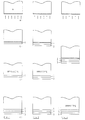
- a non-restrictive example is given in the following description of a process for metallizing a ⁇ 100> N type silicon substrate 4 doped with approximately 2 ⁇ 10 18 atoms of antimony/cm 3 (see Fig.1 ).
- an arsenic implantation is carried out using a dose of approximately 10 14 atoms/cm 3 and an energy of approximately 5 KeV (Fig. 1a), so as to produce an amorphized layer on the surface (layer indicated in the figure by the broken line).
- the substrate is then placed in an e-gun type evaporator equipped with at least three interchangeable crucibles and provided with a thermoregulated lamp heating system. After pumping to create a vacuum (with a pressure of ⁇ 1,33 ⁇ 10 -4 Pa [10 -6 Torr]), a first layer 1 of approximately 100 nm of titanium is deposited (Fig. 1b). This is followed by a heating cycle (still under high vacuum) at 375 °C for approximately thirty minutes (Fig. 1c).
- a further layer of approximately 350 nm of nickel and a film 3 of approximately 30 nm of gold are deposited (Fig. 1d).
- the entire process ensures good metallurgical characteristics and specific contact resistance values lower than approximately 10 -4 ohm ⁇ cm 2 (without the process according to this invention, there is very little likelihood of the specific contact resistance dropping below approximately 2 ⁇ 10 -2 ohm ⁇ cm 2 ).
- the annealing step which in the process of figure 1 takes place after deposition of the first metal layer, can be carried out after the second layer has been deposited ( Fig.2 ) or even after all the layers have been deposited ( Fig.3 ).
- One possible explanation for the main advantage achieved with the process according to the invention is that, in addition to producing the metal electrode of the M-S contact, the deposition of the first metal film carried out after the implantation and before the annealing treatment, also has the important function of accelerating and greatly facilitating the regrowth of the previously amorphized crystal, when the system is heated during the annealing, which can consequently be carried out at considerably low temperatures and for limited periods of time.
Landscapes
- Electrodes Of Semiconductors (AREA)
Description
Since at the end of the entire metallizing process the surface of the semiconductor will have been enriched with the appropriate species of dopant, the first layer of metal can be chosen on the basis of criteria which need not necessarily be electrical. These criteria may be better adhesion between the first layer and the semiconductor, or a better thermal expansion coefficient and less induced stress, or productivity, etc..
For some sequences of metals, depositing several metal layers in the series, or even the entire series, before annealing improves the adhesion between the various films.
- The possibility of carrying out the annealing in the same system in which the metal layers are deposited, in addition to reducing the times and cost of the necessary equipment, improves the physical properties and reliability of the metal on the back of the substrate.
- Carrying out the annealing under high vacuum conditions or in an inert atmosphere prevents oxidation or contamination of the last metal layer already deposited, thus making it possible to obtain a better interface with the metal layer deposited after the annealing;
- The possibility of considerably reducing the specific M-S contact resistance makes it possible not only to improve the electrical characteristics of the semiconductor device, but also their reproducibility; moreover, the choice of the first layer of metal is less restricted by problems of specific contact resistance thus offering the possibility of satisfying other requirements (satisfactory adhesion between the first layer and the substrate, reduction of induced stress, process economy, etc.).
Claims (6)
- Process for metallizing the back of a silicon semiconductor substrate, by depositing a series of metal layers, after ion implantation of dopant on the surface of the semiconductor which acts as an interface with the first layer of metal, said ion implantation of dopant being carried out in such a way as to amorphize the surface of the semiconductor substrate, characterized by the fact that said ion implantation is followed by:the deposition of one or more layers of metal of the aforesaid series, the metal of the first layer being titanium, and then bya thermal annealing under vacuum or in an inert atmosphere, at a temperature and for a period sufficient for regrowth of the amorphized layer and activation of the implanted species, said temperature being lower than 500 °C and said period being shorter than 60 minutes, and lastly bythe deposition of the remaining metal -layers of the series.
- Process as claimed in Claim 1, characterized by the fact that the deposition of the metal layers and the thermal annealing are carried out in the same equipment suitable for sequential deposition of several layers of metal on a semiconductor substrate and for heating the same substrate under vacuum or in an inert atmosphere.
- Process as claimed in Claim 1, characterized by the fact that the thermal annealing is carried out in a high-vacuum atmosphere with a pressure of ≤ 1,33·10-4 Pa (10-6 Torr), at a temperature of ≤ 400 °C and for a period of ≤ 30 minutes.
- Process as claimed in Claim 1, characterized by the fact that the thermal annealing is carried out in an atmosphere consisting of inert gas at a pressure of ≤ 4 Pa (30·10-3 Torr), at a temperature of ≤ 400 °C and for a period of ≤ 30 minutes.
- Process as claimed in Claim 1, characterized by the fact that the substrate is of N type, the implanted dopant is arsenic and the implantation energy is ≤ 10 KeV.
- Process as claimed in Claim 5, characterized by the fact that the dose of arsenic implanted is 2·1014 atoms/cm2, the implantation energy is 5 KeV, and the thermal annealing is carried out at a temperature of 375 °C for a period of 30 minutes.
Priority Applications (4)
| Application Number | Priority Date | Filing Date | Title |
|---|---|---|---|
| DE69033234T DE69033234T2 (en) | 1990-02-20 | 1990-02-20 | Process for multilayer metallization of the back of a semiconductor wafer |
| EP90830062A EP0443296B1 (en) | 1990-02-20 | 1990-02-20 | Process for obtaining multilayer metallization of the back of a semiconductor substrate |
| JP3045549A JP2989914B2 (en) | 1990-02-20 | 1991-02-20 | Semiconductor Substrate Backside Metallization Method |
| US08/088,113 US5342793A (en) | 1990-02-20 | 1993-07-09 | Process for obtaining multi-layer metallization of the back of a semiconductor substrate |
Applications Claiming Priority (1)
| Application Number | Priority Date | Filing Date | Title |
|---|---|---|---|
| EP90830062A EP0443296B1 (en) | 1990-02-20 | 1990-02-20 | Process for obtaining multilayer metallization of the back of a semiconductor substrate |
Publications (2)
| Publication Number | Publication Date |
|---|---|
| EP0443296A1 EP0443296A1 (en) | 1991-08-28 |
| EP0443296B1 true EP0443296B1 (en) | 1999-08-04 |
Family
ID=8205990
Family Applications (1)
| Application Number | Title | Priority Date | Filing Date |
|---|---|---|---|
| EP90830062A Expired - Lifetime EP0443296B1 (en) | 1990-02-20 | 1990-02-20 | Process for obtaining multilayer metallization of the back of a semiconductor substrate |
Country Status (3)
| Country | Link |
|---|---|
| EP (1) | EP0443296B1 (en) |
| JP (1) | JP2989914B2 (en) |
| DE (1) | DE69033234T2 (en) |
Families Citing this family (3)
| Publication number | Priority date | Publication date | Assignee | Title |
|---|---|---|---|---|
| KR960002061B1 (en) * | 1992-10-05 | 1996-02-10 | 삼성전자주식회사 | Metalization method of semiconductor device |
| JP2011029423A (en) * | 2009-07-27 | 2011-02-10 | Renesas Electronics Corp | Method of manufacturing semiconductor device |
| KR101923127B1 (en) | 2011-09-08 | 2018-11-28 | 후지 덴키 가부시키가이샤 | Semiconductor device and method for manufacturing semiconductor device |
Citations (1)
| Publication number | Priority date | Publication date | Assignee | Title |
|---|---|---|---|---|
| US4135292A (en) * | 1976-07-06 | 1979-01-23 | Intersil, Inc. | Integrated circuit contact and method for fabricating the same |
Family Cites Families (2)
| Publication number | Priority date | Publication date | Assignee | Title |
|---|---|---|---|---|
| JPS5580219A (en) * | 1978-12-06 | 1980-06-17 | Ibm | Method of forming metallic contact |
| IT1217278B (en) * | 1982-07-29 | 1990-03-22 | Ates Componenti Elettron | METALLIZATION PROCESS OF THE BACK OF A SLICE OF SILICON |
-
1990
- 1990-02-20 EP EP90830062A patent/EP0443296B1/en not_active Expired - Lifetime
- 1990-02-20 DE DE69033234T patent/DE69033234T2/en not_active Expired - Fee Related
-
1991
- 1991-02-20 JP JP3045549A patent/JP2989914B2/en not_active Expired - Fee Related
Patent Citations (1)
| Publication number | Priority date | Publication date | Assignee | Title |
|---|---|---|---|---|
| US4135292A (en) * | 1976-07-06 | 1979-01-23 | Intersil, Inc. | Integrated circuit contact and method for fabricating the same |
Non-Patent Citations (1)
| Title |
|---|
| IBM Journal of Research and Development, Vol.31, Nr.6, November 1987, pages 608-616 * |
Also Published As
| Publication number | Publication date |
|---|---|
| DE69033234T2 (en) | 2000-02-03 |
| DE69033234D1 (en) | 1999-09-09 |
| JP2989914B2 (en) | 1999-12-13 |
| EP0443296A1 (en) | 1991-08-28 |
| JPH04214671A (en) | 1992-08-05 |
Similar Documents
| Publication | Publication Date | Title |
|---|---|---|
| US4478881A (en) | Tungsten barrier contact | |
| JP3704427B2 (en) | Method for forming copper metal wiring of semiconductor device | |
| JPH08316321A (en) | Method for forming diffusion barrier film of semiconductor device | |
| EP0053712A1 (en) | Method of improving the conductivity of a microelectronic conductive tungsten silicide film and semiconductor device comprising said film | |
| KR20030044800A (en) | Semiconductor device having a low-resistance gate electrode | |
| EP0085918A2 (en) | Metallic silicide production | |
| JP3079851B2 (en) | Method for manufacturing silicon carbide electronic device | |
| JPH05102072A (en) | Semiconductor device including silicide layer and method of manufacturing the device | |
| JPH03110837A (en) | Manufacture of semiconductor device | |
| US5342793A (en) | Process for obtaining multi-layer metallization of the back of a semiconductor substrate | |
| EP0443297B1 (en) | Metal-semiconductor ohmic contact forming process | |
| KR20040015670A (en) | Depositing a Tantalum Film | |
| EP0443296A1 (en) | Process for obtaining multilayer metallization of the back of a semiconductor substrate | |
| JP2002525870A (en) | Method of forming ohmic contact | |
| JP3488586B2 (en) | Method for manufacturing semiconductor device | |
| Andersson et al. | Electrical characteristics of sputtering-induced defects in n-type silicon | |
| JP2004525257A (en) | Method for obtaining low temperature alpha tantalum thin film using wafer bias | |
| JPH01179415A (en) | Metal silicide layer forming method | |
| US5877031A (en) | Method for forming a metallic barrier layer in semiconductor device | |
| JP2542617B2 (en) | Method for manufacturing semiconductor device | |
| JP3245269B2 (en) | Method for manufacturing semiconductor device | |
| Lue | Formation of nickel and palladium silicides by a short-pulse light-flash and its application in the metallization of solar cells | |
| US5418188A (en) | Method for controlled positioning of a compound layer in a multilayer device | |
| JPH06140358A (en) | Manufacture of semiconductor device | |
| Vaidya | Electromigration in aluminum/poly‐silicon composites |
Legal Events
| Date | Code | Title | Description |
|---|---|---|---|
| PUAI | Public reference made under article 153(3) epc to a published international application that has entered the european phase |
Free format text: ORIGINAL CODE: 0009012 |
|
| AK | Designated contracting states |
Kind code of ref document: A1 Designated state(s): DE FR GB IT NL |
|
| 17P | Request for examination filed |
Effective date: 19920307 |
|
| 17Q | First examination report despatched |
Effective date: 19921116 |
|
| GRAG | Despatch of communication of intention to grant |
Free format text: ORIGINAL CODE: EPIDOS AGRA |
|
| GRAG | Despatch of communication of intention to grant |
Free format text: ORIGINAL CODE: EPIDOS AGRA |
|
| GRAH | Despatch of communication of intention to grant a patent |
Free format text: ORIGINAL CODE: EPIDOS IGRA |
|
| RAP3 | Party data changed (applicant data changed or rights of an application transferred) |
Owner name: STMICROELECTRONICS S.R.L. |
|
| GRAH | Despatch of communication of intention to grant a patent |
Free format text: ORIGINAL CODE: EPIDOS IGRA |
|
| GRAA | (expected) grant |
Free format text: ORIGINAL CODE: 0009210 |
|
| AK | Designated contracting states |
Kind code of ref document: B1 Designated state(s): DE FR GB IT NL |
|
| PG25 | Lapsed in a contracting state [announced via postgrant information from national office to epo] |
Ref country code: NL Free format text: LAPSE BECAUSE OF FAILURE TO SUBMIT A TRANSLATION OF THE DESCRIPTION OR TO PAY THE FEE WITHIN THE PRESCRIBED TIME-LIMIT Effective date: 19990804 |
|
| REF | Corresponds to: |
Ref document number: 69033234 Country of ref document: DE Date of ref document: 19990909 |
|
| ITF | It: translation for a ep patent filed | ||
| ET | Fr: translation filed | ||
| NLV1 | Nl: lapsed or annulled due to failure to fulfill the requirements of art. 29p and 29m of the patents act | ||
| PLBE | No opposition filed within time limit |
Free format text: ORIGINAL CODE: 0009261 |
|
| STAA | Information on the status of an ep patent application or granted ep patent |
Free format text: STATUS: NO OPPOSITION FILED WITHIN TIME LIMIT |
|
| 26N | No opposition filed | ||
| REG | Reference to a national code |
Ref country code: GB Ref legal event code: IF02 |
|
| PGFP | Annual fee paid to national office [announced via postgrant information from national office to epo] |
Ref country code: FR Payment date: 20020212 Year of fee payment: 13 |
|
| PGFP | Annual fee paid to national office [announced via postgrant information from national office to epo] |
Ref country code: GB Payment date: 20020220 Year of fee payment: 13 |
|
| PGFP | Annual fee paid to national office [announced via postgrant information from national office to epo] |
Ref country code: DE Payment date: 20020306 Year of fee payment: 13 |
|
| PG25 | Lapsed in a contracting state [announced via postgrant information from national office to epo] |
Ref country code: GB Free format text: LAPSE BECAUSE OF NON-PAYMENT OF DUE FEES Effective date: 20030220 |
|
| PG25 | Lapsed in a contracting state [announced via postgrant information from national office to epo] |
Ref country code: DE Free format text: LAPSE BECAUSE OF NON-PAYMENT OF DUE FEES Effective date: 20030902 |
|
| GBPC | Gb: european patent ceased through non-payment of renewal fee | ||
| PG25 | Lapsed in a contracting state [announced via postgrant information from national office to epo] |
Ref country code: FR Free format text: LAPSE BECAUSE OF NON-PAYMENT OF DUE FEES Effective date: 20031031 |
|
| REG | Reference to a national code |
Ref country code: FR Ref legal event code: ST |
|
| PG25 | Lapsed in a contracting state [announced via postgrant information from national office to epo] |
Ref country code: IT Free format text: LAPSE BECAUSE OF NON-PAYMENT OF DUE FEES;WARNING: LAPSES OF ITALIAN PATENTS WITH EFFECTIVE DATE BEFORE 2007 MAY HAVE OCCURRED AT ANY TIME BEFORE 2007. THE CORRECT EFFECTIVE DATE MAY BE DIFFERENT FROM THE ONE RECORDED. Effective date: 20050220 |