EP0438119A2 - Numerische Verarbeitung von optischen Wellenfrontdaten - Google Patents
Numerische Verarbeitung von optischen Wellenfrontdaten Download PDFInfo
- Publication number
- EP0438119A2 EP0438119A2 EP91100414A EP91100414A EP0438119A2 EP 0438119 A2 EP0438119 A2 EP 0438119A2 EP 91100414 A EP91100414 A EP 91100414A EP 91100414 A EP91100414 A EP 91100414A EP 0438119 A2 EP0438119 A2 EP 0438119A2
- Authority
- EP
- European Patent Office
- Prior art keywords
- processing nodes
- data
- kth
- array
- node
- Prior art date
- Legal status (The legal status is an assumption and is not a legal conclusion. Google has not performed a legal analysis and makes no representation as to the accuracy of the status listed.)
- Withdrawn
Links
Images

Classifications
-
- G—PHYSICS
- G06—COMPUTING OR CALCULATING; COUNTING
- G06E—OPTICAL COMPUTING DEVICES; COMPUTING DEVICES USING OTHER RADIATIONS WITH SIMILAR PROPERTIES
- G06E1/00—Devices for processing exclusively digital data
- G06E1/02—Devices for processing exclusively digital data operating upon the order or content of the data handled
Definitions
- the field of the invention is that of adaptive optics, in particular, the subfield of measurement of optical wavefronts and computation of solutions to the wave equation.
- the art has long sought a fast digital technique to solving the wave equations that is suitable for real time systems involving large numbers of data points.
- the invention relates to a hardware system for reconstructing the wavefront of a sample beam in which a parallel array of processors operates with a novel method to solve the wave equation in a number of operations that is essentially proportional to the number of sample points.
- Fig. 1 illustrates an overall optical system in which the invention is to be used.
- Fig. 2 illustrates in schematic form an implementation of a processor array according to the invention.
- Fig. 3 illustrates a detail from the system of Fig. 2.
- Fig. 4 illustrates a logical block diagram of an individual processor.
- Fig. 5 illustrates a sequence of operations of transforming data according to the invention.
- Fig. 6 illustrates pictorially the relationships of different sets of data points used in processing according to the invention.
- Fig. 7 illustrates schematically an interconnection scheme for different processors using the approach illustrated in Fig. 6.
- Fig. 8 illustrates a prototype processor module useful in constructing systems according to the invention.
- Fig. 9 illustrates intermediate steps in Fig. 5.
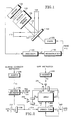
- FIG. 1 there is illustrated an overall system in which an input optical beam 110 strikes a deformable mirror 125 having a flexible surface 127 that can be adjusted in order to correct for deviations in the wavefront of beam 110.
- the bulk of the beam goes out as beam 120, but a sample beam is tapped off by beam sampling surface 127 and is shown as sample beam 115 entering a Hartmann or other wavefront sensor, indicated by block 130.
- Such sensors are well known in the art and may be that illustrated in U. S. Patent 4,399,356 or any other convenient sensor.
- the detector associated with the sensor is indicated by block 132, which represents an array of N detectors, such as quadrant detectors, that will produce electrical signals going to digitizer 135, that converts the analog signals from the detectors to digital representations of those values.
- the digital representations then go to processor 140 which compares adjacent sensors and sends a digital representation of the tilt of the wavefront (or the derivative of the phase) to reconstructor 150, which will be constructed according to the invention.
- the output of reconstructor 150 is a set of signals going to driver 160 which translates between the representation of the phase coming from reconstructor 150 to a set of signals corresponding to the drivers on the flexible surface of deformable mirror 125.
- Driver 160 then stretches or compresses the actuators in mirror 125 to control the surface 127 to produce the desired phase change.
- reconstructor 150 there will be an array of parallel processing nodes, one for each sensor in digitizer 135. These processing nodes will be arranged in a rectangular array, each member of which will have a local memory having different memory addresses, an ALU for executing different instructions to shift, add, etc., and input/output hardware for shifting data to different nodes.
- Reconstruction is the operation that converts a set of discretely sampled values representing the X and Y directional derivatives of an optical wavefront into another set of numbers representing the discrete values of the phases of this wavefront as they might be measured on another grid, such as one centered on the locations of actuators on a deformable mirror.
- the reconstruction problem can be thought of as the problem of solving the discretized version of a partial differential equation subject to various types of boundary conditions.
- the problem could also be thought of as the solution to a matrix equation whose solution is mathematically straight forward.
- the dimensions of the matrix will be proportional to the number of input measurement points times the number of output points. In a typical system, these will be the number of input points where wavefront measurements are made and the number of output points represented as 2N and N, respectively.
- the factor of two comes from the measurement of both X and Y coordinates.
- the number of matrix elements in the matrix will be therefore proportional to N2.
- the displacement of the reflective surface is described by Poisson's equation.
- the iterative method of obtaining a solution to the Poisson equation is simply to proceed through the array of sample points and to assign to each sample point within the region a value equal to the average of the surrounding four sample points. Multiple passes through the array of points should cause the average value at a sample point to converge to the solution of the finite difference equation.
- Equation 1 illustrates an approximation in which P k (x,y) is the kth approximation to Poisson's equation, the P k-1 (x,y) are the approximate versions at the points x,y for the previous iteration, and d(g x ,g y ) is a function of the external gradients as measured by the wavefront processor. It has been found that the deviation between the approximate solution and the true solution is of the form indicated by Equation 2. (2) Error RMS ⁇ 10 -aI/N , where I is the number of iterations, N is the number of data points, and a is a proportionality constant.
- the approach taken is to compress the data by forming an average value for a set of neighboring data points and to repeat this averaging process as many times as required to compress the data to a number of points that may be handled by an array of parallel processors of reasonable size.
- This final set of compressed data is the input to an iterative solution of Poisson's equation. That initial solution is used in an expansion process that is the inverse of the compression process. At the kth iteration level, the values of (k-1)th level solution are replicated to form an initial approximation for the kth level.
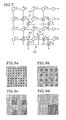
- Fig. 5(a) illustrates a 16x16 array of data points, each of which represents both a point on a reference surface on a phase front and also an individual processing node in an array that will be described below.
- these data points have been reduced to one quarter of the number by substituting for each point in Fig. 5(b) the average of four neighboring points in Fig. 5(a).
- the point in the lower right-hand corner of each group of four points was chosen to carry the average value of that group of points.
- This point or another conventional point will be referred to as the transfer member of the set.
- this new second set of data points has been transferred to another contiguous array, now having dimension 8x8.
- the process of compression is repeated a second time to form a 4x4 array.
- This first solution has as input data a set of sixteen points that are the result of two successive averagings and thus contain only the coarsest features of the input data. It is this solution that will represent the overall large-scale features of the final solution to the equations.
- Fig. 5(g) illustrates the first step, in which the value of each of the sixteen points is copied or replicated to corresponding points in an 8x8 array and then duplicated in a square of four points.
- the 4x4 array for the first solution is transformed to a 8x8 array, in which groups of four processors have the identical input data.
- the equations are then solved on this 8x8 array of processors, using the replicated data as the first approximation and the averaged data from the first array for the boundary conditions, to result at the second solution.
- This second solution will result from a variable number of iterations, depending upon the convergence criterion being used and the shape of the phase front.
- each point on the array is a processing node including a node processor that will be an ALU and node input/output ports connected to adjacent processing nodes and local node storage, quite a bit of time is required to pass the data through the several processors in order to carry out the 4x4 average and to shift the averaged points to a contiguous array (and the inverse processes).
- the array is then ANDed with a mask that has a value of zero for those points (A11, A12, A21 in this set of four points) that are no longer needed and a value of one for the points to be preserved, (A22).
- the result of the masking operation is that only the processing nodes in the lower right corner of each group of four will have a non-zero value.
- Fig. 9b The process of further compression that transforms Fig. 5b to Fig. 5c is illustrated in Fig. 9.
- the same steps of addition listed above are used to shift the data to the intermediate positions shown in Fig. 9b. Since the "white" positions contain the value zero, the values of the data are not affected during the shift.
- the new value of A33 is that of the old value of A22, because the intermediate points have the value zero.
- the new value of A44 is its old value, because only zeroes were added to it.
- a xy A (x-2)y + A xy , which transforms to the configuration of Fig. 9c.
- (x-2)y is that the data in processing node x,y has added to it the data from the node two positions to the left.
- the particular hardware used has a pass through facility that permits the transfer of data through an intermediate processing element without affecting the data in that intermediate element.
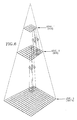
- Fig. 6 illustrates an alternative version of a processor in which the processing nodes are arranged in different "planes" that can operate simultaneously.
- the bottom level of the "pyramid” is the 16x16 original array; the middle level is the 8x8 array; and the top level is the final 4x4 array.
- corresponding points in the compression sequence are connected by wires extending upwardly from one array to another, so that the data is transferred from a lower-right-hand-corner processing node, referred to as a "transfer node" to a corresponding node in the next level without being shifted through additional processing nodes. In hardware, this would be implemented by connections between different printed circuit boards.
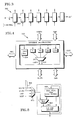
- FIG. 2 there is a representation of a level of the pyramid of Fig. 6.
- Data enters on line 212 to buffer 206, then passes on line 214 to the input to the array of processors formed in a single integrated circuit 250.
- This input is indicated as box 220, the contents of which will be discussed below.
- the data enters array 250, illustratively a 6x12 array of processors. Lines around the outside of box 250 indicate the transfers may be "looped" around from North to South and vice versa and from East to West and vice versa. This is not essential, but is a great convenience in moving data between the various nodes.
- the two sets of buffers and controllable terminal 252 and 254 are used to force data into the edges of array 250.
- the terminal may be set at logic zero or logic one and the buffers may be set to pass that value to either or both sides of the array.
- This array is constructed from commercially available unit, the NCR45CG72 "GAPP" chip, available from the National Cash Register Corporation, which include a CMOS systolic array with 72 single bit processors per chip, arranged as a grid of 6x12, organized on the principle of single instruction multiple data; i.e., all the processors execute the same instruction at the same time on the data that is present at their nodes.
- Box 240 is a register for storing the instruction to be delivered to all the processors.
- address generator 230 generates an address within local memory, common to the whole array, which may contain stored data or a stored instruction sequence.
- Fig. 3 illustrates the contents of "corner turn" box 220 which performs a parallel to serial conversion and also performs shift register functions.
- data enters from line 214 as a set of six eight-bit words in this particular embodiment, which are loaded sequentially into the various modules 222. These words are then shifted one bit at a time serially up in the Figure on the lines labeled CMS 0-5 and enter the bottom portion of array 250. Data coming out of the top of the array is looped around and enters in from below to individual modules 222. Data is taken out of the array by looping in from below to each of modules 222 and then by shifting in parallel a byte at a time out to the right in the Figure.
- the number of modules used in any embodiment will depend on the size of the array and the method of passing data through the individual processors in the array. In the case illustrated, the array was of dimension 6x12, so that the appropriate number of modules was six.
- control means which includes the address generator 230, GAPP instruction unit 240, a finite state machine or CPU not shown to control the sequence of instructions and associated connections.
- the term calculation means includes the processing nodes and the term shift means includes input/output ports at the processing nodes and corner turn 220.
- the nth solution generated by a single CPU was fed back in (through conventional buses, registers, memory, etc.) to the CPU to be used for the (n+1)th iteration.
- the set of hardware collectively used to effect the transfer will referred to as a feedback means.
- FIG. 4 A block diagram of a single processing element in a GAPP chip is illustrated in Fig. 4, in which ALU 252 forms the central element that is connected to other nodes through two boxes labelled NS and EW, respectively.
- the boxes represent multiplexers connected to four ports (N,S,E,W) that are general communications lines.
- the boxes labelled CMS and CMN are ports that are used to load and unload data without interfering with the processing. These units are connected to a set of six bidirectional I/O ports connected to adjacent processing elements.
- a 128x1 RAM is available for storing data, such as values shifted into this node or temporary results. Instructions are not stored locally in this embodiment, which operates on the SIMD (Single Instruction Multiple Data) principle, in which all nodes execute the same instruction simultaneously.
- SIMD Single Instruction Multiple Data
- the box labelled C is used for a carry bit and the box labelled CM is a pass through connection from the North to South ports that facilitates transfer to and from the I/O box 220 of Fig. 2. Instructions and control signals for loading data in and out of the chip are omitted from the Figure for clarity.
- the apparatus shown in Fig. 2 is controlled by any convenient means such as a general purpose computer that contains the stored instructions for generating the sequence of data transfer shifts and iterative equation solving to be described below.
- FIG. 7 An alternate version of a portion of the pyramid embodiment of Fig. 6 is illustrated in Fig 7, showing in partially schematic, partially pictorial fashion a portion of a circuit board including three levels of such a pyramid.
- Each box in the Figure is a processing node, whether one-bit or some higher number.
- the lines are buses of appropriate width for the number of bits.
- a 4x4 section of the array, the boxes of which are denoted by the letter A is the lowest level, with the boxes denoted by B being the second level and the single box denoted by a C as the third level.
- the portion shown is the upper left corner of an array that extends to some convenient distance off the paper.
- the sum in A22 may be divided by four if it is desired to keep the data in scale. Corresponding transfers take place in the other groups of four, both at the A level and at the B and C levels. Once the data is stored in the lower right corner, it is transferred between levels.
- A22 The data in A22 is transferred through node 710 to B11 and vice versa for the inverse expansion step.
- data in A24, A42, and A44 are transferred to corresponding nodes B12, B21, and B22. It doesn't matter which set of data is transferred first.
- processor nodes B11 and B12 are shown as being connected directly to a node 710 between two of the A processing nodes on the North side.
- Nodes B21 and B22 are shown as using a multiplexed input on the North side, in which one input is connected to the corresponding A node 720 and the other is a B-level bus connecting B21, to B11, etc.
- This multiplexed connection between the A and B nodes is not essential, but eliminates the need to watch the timing between the A and B levels to avoid getting data for the different levels mixed. With the A and B levels isolated, both levels can perform intra-level data transfer independently.
- the A nodes will replicate the data - the contents of A22 will be duplicated in A12, A21, and A12 - the A nodes will iterate to a solution of Poisson's equation. Simultaneously with the A level iteration, the B level will be iterating data that was passed down from the C level.
- One sequence for such a pipeline processing scheme is, for the nth level:
- each level be able to store a set of data during the iteration process, to be sent up to the next level during the inter-iteration transfer period.
- FIG. 8 there is shown in schematic form an illustration of a processing node suitable for use with the invention.
- the processor will handle a reasonable width word, such as 16 bits, but no particular number is required.
- Input multiplexer 810 has four ports corresponding to the four directions in which data will be transferred. As discussed above with respect to Fig. 7, it may be convenient to have an additional multiplexer 805, shown in dotted lines, to facilitate transfer between levels. As shown in Fig. 7, B22, for example, transfers data to and from A44, with appropriate control signals being sent to the two modules to transfer and receive the data.
- Secondary multiplexer 820 serves to direct input or output data into ALU 840 or to direct stored data from RAM 830 into the ALU.
- Ram 830 can be used to store data during iterations or in the regular ALU operation.
- An adder is insufficient because the data compression operations require masking (or an erase command).
- Multiplication capability is convenient, but not essential.
- the I/O requirement is two bidirectional ports or four unidirectional ports. As shown in Fig. 8, four bidirectional ports are preferred.
- Control of individual nodes is performed using a command common to all nodes, so that local storage of commands is not required.
- Processors on the edge will be dealing with only three neighbors instead of the usual four. This may be handled as described above by loading in zeroes for initial data to substitute for a missing neighbor.
- the system offers the additional advantage that the calculations can be weighted to favor the better data.
Landscapes
- Engineering & Computer Science (AREA)
- Theoretical Computer Science (AREA)
- Physics & Mathematics (AREA)
- General Physics & Mathematics (AREA)
- Multi Processors (AREA)
- Complex Calculations (AREA)
Applications Claiming Priority (2)
| Application Number | Priority Date | Filing Date | Title |
|---|---|---|---|
| US465297 | 1990-01-16 | ||
| US07/465,297 US5119323A (en) | 1990-01-16 | 1990-01-16 | Numerical processing of optical wavefront data |
Publications (2)
| Publication Number | Publication Date |
|---|---|
| EP0438119A2 true EP0438119A2 (de) | 1991-07-24 |
| EP0438119A3 EP0438119A3 (en) | 1992-10-28 |
Family
ID=23847222
Family Applications (1)
| Application Number | Title | Priority Date | Filing Date |
|---|---|---|---|
| EP19910100414 Withdrawn EP0438119A3 (en) | 1990-01-16 | 1991-01-15 | Numerical processing of optical wavefront data |
Country Status (3)
| Country | Link |
|---|---|
| US (1) | US5119323A (de) |
| EP (1) | EP0438119A3 (de) |
| JP (1) | JPH0528177A (de) |
Families Citing this family (5)
| Publication number | Priority date | Publication date | Assignee | Title |
|---|---|---|---|---|
| US6298162B1 (en) * | 1992-12-23 | 2001-10-02 | Lockheed Martin Corporation | Image compression/expansion using parallel decomposition/recomposition |
| US5937202A (en) * | 1993-02-11 | 1999-08-10 | 3-D Computing, Inc. | High-speed, parallel, processor architecture for front-end electronics, based on a single type of ASIC, and method use thereof |
| US5978794A (en) * | 1996-04-09 | 1999-11-02 | International Business Machines Corporation | Method and system for performing spatial similarity joins on high-dimensional points |
| US5912815A (en) * | 1997-03-14 | 1999-06-15 | The Regents Of The University Of California | Local relaxation method for estimating optical flow |
| US7051309B1 (en) * | 1999-02-16 | 2006-05-23 | Crosetto Dario B | Implementation of fast data processing with mixed-signal and purely digital 3D-flow processing boars |
Family Cites Families (4)
| Publication number | Priority date | Publication date | Assignee | Title |
|---|---|---|---|---|
| JPS60136875A (ja) * | 1983-12-26 | 1985-07-20 | Hitachi Ltd | ベクトル演算器 |
| JP2617733B2 (ja) * | 1986-09-09 | 1997-06-04 | 株式会社日立製作所 | 初等関数演算装置 |
| US4823299A (en) * | 1987-04-01 | 1989-04-18 | The United States Of America As Represented By The Administrator Of The National Aeronautics And Space Administration | Systolic VLSI array for implementing the Kalman filter algorithm |
| US4858147A (en) * | 1987-06-15 | 1989-08-15 | Unisys Corporation | Special purpose neurocomputer system for solving optimization problems |
-
1990
- 1990-01-16 US US07/465,297 patent/US5119323A/en not_active Expired - Fee Related
-
1991
- 1991-01-15 EP EP19910100414 patent/EP0438119A3/en not_active Withdrawn
- 1991-01-16 JP JP3015919A patent/JPH0528177A/ja active Pending
Non-Patent Citations (5)
| Title |
|---|
| HWANG ET AL 'Computer Architecture and Parallel Processing' 1988 , MCGRAW-HILL , NEW YORK, US * |
| ICASSP 88, April 11-14 1988, New York, US, pp812 -815; Wang et al: 'Pyramid transform coding using vec tor quantization' * |
| MICROPROCESSING AND MICROPROGRAMMING. vol. 20, no. 1-3, April 1987, AMSTERDAM NL pages 113 - 118; SIVA RAM MURTHY ET AL: 'A Multi-Microprocessor Architecture for solving Partial Differential Equations' * |
| PARALLEL COMPUTING. vol. 12, no. 2, November 1989, AMSTERDAM NL pages 131 - 144; HART ET AL: 'Asynchronous multilevel adaptive methods for solving partial differential equations on multiprocessors: Basic ideas' * |
| Proceedings, 7th Symposium on Computer Arithme- tic, June 4-6 1985, Urbana, Ill, US, pp252-259; Gannon: 'On the structure of parallelism in a highly concurrent PDE solver' * |
Also Published As
| Publication number | Publication date |
|---|---|
| US5119323A (en) | 1992-06-02 |
| EP0438119A3 (en) | 1992-10-28 |
| JPH0528177A (ja) | 1993-02-05 |
Similar Documents
| Publication | Publication Date | Title |
|---|---|---|
| EP2017743B1 (de) | Effizientes Hochgeschwindigkeitshardwaremodul zur Matrizenmultiplikation | |
| Kung | Special-purpose devices for signal and image processing: an opportunity in very large scale integration (VLSI) | |
| Ebeling et al. | Mapping applications to the RaPiD configurable architecture | |
| US5659780A (en) | Pipelined SIMD-systolic array processor and methods thereof | |
| US4821224A (en) | Method and apparatus for processing multi-dimensional data to obtain a Fourier transform | |
| EP0479102A2 (de) | Multidimensionale systolische Matrix | |
| Kung | Computational models for parallel computers | |
| JPH0612393A (ja) | マルチプロセッサデータ処理システム | |
| JPH03209561A (ja) | 連立一次方程式の解を求める計算装置及び方法 | |
| US5119323A (en) | Numerical processing of optical wavefront data | |
| Taylor et al. | An architecture for a video rate two-dimensional fast Fourier transform processor | |
| Annaratone et al. | Using Warp as a supercomputer in signal processing | |
| Albanesi et al. | A high speed Haar transform implementation | |
| Hsu | LINC: The link and interconnection chip | |
| Roditis et al. | Parallel multisplitting, block Jacobi type solutions of linear systems of equations | |
| Yeh et al. | A class of parallel architectures for fast Fourier transform | |
| Kung | Warp experience: we can map computations onto a parallel computer efficiently | |
| Wojtek Przytula et al. | Parallel implementation of neural networks | |
| Hammond et al. | Architecture and operation of a systolic engine for finite element computations | |
| Lawson et al. | SMART: a neurocomputer using sparse matrices | |
| Anand et al. | BrahMap: A scalable and modular map-making framework for the CMB experiments | |
| Liu et al. | A bit-serial VLSI architecture for generating moments in real-time | |
| Shivaprasad et al. | Design and implementation of parallel floating point matrix multiplier for quaternion computation | |
| Lattard et al. | Massively parallel architecture: application to neural net emulation and image reconstruction | |
| Bowden | Kron's method of tearing on a transputer array |
Legal Events
| Date | Code | Title | Description |
|---|---|---|---|
| PUAI | Public reference made under article 153(3) epc to a published international application that has entered the european phase |
Free format text: ORIGINAL CODE: 0009012 |
|
| AK | Designated contracting states |
Kind code of ref document: A2 Designated state(s): DE FR GB |
|
| PUAL | Search report despatched |
Free format text: ORIGINAL CODE: 0009013 |
|
| AK | Designated contracting states |
Kind code of ref document: A3 Designated state(s): DE FR GB |
|
| 17P | Request for examination filed |
Effective date: 19921201 |
|
| 17Q | First examination report despatched |
Effective date: 19950227 |
|
| STAA | Information on the status of an ep patent application or granted ep patent |
Free format text: STATUS: THE APPLICATION IS DEEMED TO BE WITHDRAWN |
|
| 18D | Application deemed to be withdrawn |
Effective date: 19960801 |