EP0436704B1 - Modulator circuit - Google Patents
Modulator circuit Download PDFInfo
- Publication number
- EP0436704B1 EP0436704B1 EP90911760A EP90911760A EP0436704B1 EP 0436704 B1 EP0436704 B1 EP 0436704B1 EP 90911760 A EP90911760 A EP 90911760A EP 90911760 A EP90911760 A EP 90911760A EP 0436704 B1 EP0436704 B1 EP 0436704B1
- Authority
- EP
- European Patent Office
- Prior art keywords
- circuit
- signal
- carrier wave
- phase
- vector
- Prior art date
- Legal status (The legal status is an assumption and is not a legal conclusion. Google has not performed a legal analysis and makes no representation as to the accuracy of the status listed.)
- Expired - Lifetime
Links
Images

Classifications
-
- H—ELECTRICITY
- H03—ELECTRONIC CIRCUITRY
- H03C—MODULATION
- H03C3/00—Angle modulation
- H03C3/38—Angle modulation by converting amplitude modulation to angle modulation
- H03C3/40—Angle modulation by converting amplitude modulation to angle modulation using two signal paths the outputs of which have a predetermined phase difference and at least one output being amplitude-modulated
-
- H—ELECTRICITY
- H03—ELECTRONIC CIRCUITRY
- H03C—MODULATION
- H03C5/00—Amplitude modulation and angle modulation produced simultaneously or at will by the same modulating signal
Definitions
- This invention relates to a modulator circuit, particularly though not exclusively for modulating sound signals onto a carrier wave for a video recorder system.
- Video recorder systems commonly use a method of FM modulation for modulating an audio frequency (AF) input signal onto a sub-carrier of the video system.
- FM modulators commonly comprise a resonant circuit, such as an L-C circuit with a variable capacitance provided usually in the form of a varactor diode for modulating the resonant frequency of the circuit.
- a resonant circuit such as an L-C circuit with a variable capacitance provided usually in the form of a varactor diode for modulating the resonant frequency of the circuit.
- One problem with such circuit is that for hi-fidelity reproduction a relatively large deviation or bandwidth is required (75 Kilohertz), and the simple modulating circuit may well introduce non-linearities.
- the object of the present invention is to provide a modulator circuit which can simply be switched between an FM mode of operation and an AM mode of operation depending on the television standard with which the modulator is to be used, and which desirably provides linear modulation over a wide deviation range.
- the present invention is based on the recognition that in order to provide an AM mode of operation, a mixer circuit is required to mix the audio frequency (AF) signal with the carrier wave signal, and that this audio modulated signal may be employed to generate a frequency modulated signal by shifting the audio modulated signal in phase and adding the phase shifted signal to the carrier wave signal in order to generate the FM signal.
- AF audio frequency
- Prior arrangements utilising this principle are disclosed for example in United States Patent Nos. 3,002,159 and 3,378,773.
- a modulator circuit comprises an input for receiving an audio frequency signal, an oscillator circuit for providing a carrier wave signal, a mixer circuit for mixing the audio frequency signal with the carrier wave signal to provide an amplitude modulated signal, phase shift means for shifting the phase of the amplitude modulated signal relative to the carrier wave signal, and vector adding means for adding the phase-shifted amplitude modulated signal and the carrier wave signal, characterised in that said oscillator circuit includes transistor means having a resonant circuit connected as a collector load, the oscillator circuit having a linear phase versus frequency characteristic over a predetermined range of frequencies, and that the vector adding means comprises a nodal connection for coupling said phase-shifted amplitude modulated signal to said collector load, whereby said oscillator circuit provides a carrier wave signal frequency modulated with said audio frequency signal.
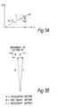
- Figure la shows a conventional representation of the frequency modulation process in the complex plane wherein the carrier wave is represented by a vector C which rotates in an anti-clockwise direction with an angular velocity ⁇ c and the modulating signal is represented by a vector M which is added to vector C and which rotates about the end of vector C with the modulation angular velocity ⁇ m .
- the projection of the vector sum on the x coordinate represents the real value of the amplitude of the signal at any given moment.
- the output signal is of constant amplitude but its frequency varies cyclically, the maximum frequency deviation being proportional to the amplitude of the modulating signal M and the rate of change of the frequency deviation being proportional to the frequency of the modulating signal M.
- a frequency modulated signal is synthesised by adding to the carrier wave amplitude a vector which is wholly or has a substantial component at right angles to the amplitude vector, such vector having a length proportional to the instantaneous real value of the AF modulating input.
- a vector which is wholly or has a substantial component at right angles to the amplitude vector, such vector having a length proportional to the instantaneous real value of the AF modulating input.
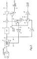
- FIG 2 there is shown a modulator circuit in accordance with the invention for use in a video recorder wherein the sound is added to the video signal by means of a separate sub-carrier.
- the circuit shown is adapted to be formed on a single integrated circuit, and an oscillator 2 is formed so that components 4 may be added to the integrated circuit for determining the operating frequency of the oscillator, such as a tank coil or a crystal.
- Oscillator 2 is connected to an input 40 of a vector adder circuit 6, described below with reference to figure 3, and a 90° phase shift circuit 8, which may be a simple R-C network or an active network.
- Phase shift network 8 is connected to a mixer 10 of suitable form, for example a diode ring or balanced quad where it is mixed with an audio frequency input signal at a terminal 12 coupled to a preamplifier 14 whose output is fed to mixer 10.
- the gain of amplifier 14 is controlled by a control line 16 via a switch 18.
- the output of mixer 10 is applied to a two pole switch 20, one output of the switch being coupled via a gain control amplifier 22 to a further switch 24 to which an output line 26 is coupled having a gain control amplifier 28.
- Switches 18, 20, 24 are controlled by a single input line 30, termed "AM/FM select".
- the other output of switch 20 is coupled to a feedback loop 32 having a feedback amplifier 34 to a second input 42 of vector adder circuit 6.
- the output of vector adder circuit 6 is coupled via an output line 35 and gain control amplifier 36 to the other input of switch 24.
- the vector adder circuit may be of any convenient form, for example a nodal summing connection.
- the AM/FM select line 30 is actuated to determine whether AM or FM modulation is to be produced.
- switch 20 couples mixer 10 to feedback line 32 and switch 24 couples output line 26 to FM output line 35.
- the output vector C available on line 35 is shifted in phase by 90° in phase shifter circuit 8 and applied to one input of mixer 10 where it is mixed with the modulating AF input signal.
- the output of mixer 10 is a vector at right angles to the carrier wave signal and has an amplitude which is proportional to the AF input signal. This signal is represented by vector B in figure 1b. This signal is applied via feedback line 32 to input 42 of the vector adder circuit 6.
- Vector adder circuit 6 is operative above to add the carrier wave vector A to the modulating vector B to produce the output vector C which is available on line 35 and is applied via gain control amplifier 36 to the output line 26.
- the output of the oscillator 2 is modulated in phase by the addition of vector B to provide a resultant FM modulation.
- select line 30 is suitably actuated so that switch 18 is coupled to control line 16, switch 20 is coupled to amplifier 22 and feedback line 32 is disabled, and amplifier 22 is coupled to output line 26.
- This is the AM mode of operation and the signal on control line 16 controls the modulation depth of the modulating signal applied to mixer 10.
- the carrier wave from oscillator 2 is applied to the other input of mixer 10 via vector adder circuit 6, vector adder circuit 6 however being disabled since no input is provided on feedback line 32.
- a conventional mixing process is provided and the AM modulated signal is provided at the output from mixer 10 to output line 26.
- FIG. 3 it shows a second embodiment of the invention, similar parts to those of Figure 2 are indicated by the same reference numeral.
- the embodiment of Figure 3 differs principally in the oscillator circuit 2 being driven by the output of vector adder circuit 6. with the input 40 of vector adder circuit 6 being provided with an output signal from the oscillator 2 via a feedback loop 50 containing a gain control amplifier 52.
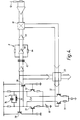
- phase shift circuit 8 is provided by a transimpedance amplifier 60 coupled to phase shift capacitors 62 and having feedback resistors 64.
- a voltage to current converter circuit 66 is provided for providing a signal to the mixer circuit 10.
- the feedback signal on line 32 is fed to a differential amplifier drive circuit 70 whose collectors are coupled to the collectors of a differential pair 72 of an oscillator circuit 6, the oscillator circuit having a resonant circuit 4 comprising a capacitor 74 and an inductance 76 coupled between the collectors of the differential pair 72.
- the collectors of the differential pair 72 are cross-coupled to the respective bases via transistors 78.
- the differential pair 72 has a current source 80 in the tail which is controlled by an automatic gain control circuit.
- oscillations are sustained in the absence of modulation by the positive feedback loops back to the bases of transistors 72.
- signals are provided via drive circuit 70 to the collectors of pair 72, which modulating signals are 180° out of phase with each other and 90° out of phase with the oscillator signal generated within oscillator 2.
- the connection to the collectors of transistor pair 72 thus provides a vector adding circuit and the modulated signals added to the resonant circuit provide frequency deviation from the resonant frequency, and by virtue of the linear phase versus frequency response of the circuit over a predetermined ranges a frequency deviation is generated within the oscillator which is proportional to the phase deviation provided by the modulated signal.
- this invention relates to a design of modulator circuit capable of producing both AM or FM modulated outputs and is designed to be very suitable for up integration. It is principally intended for performing the sound sub-carrier modulation in video modulator circuits, though will have applications wherever a good AM and/or FM modulation is required.
- the circuit is designed with minimum external components, simply requiring an external tank coil for the oscillator section. It is also designed to be simple in it's application having one AF input for both modulation types and one RF output. A further input is provided for setting the AM modulation depth; in the intended video modulator application this would be a fixed level so would come from an internally generated source. The setting of the AM modulation depth can be achieved through the AF input if a further input is not wanted. The modulation generated is simply selected by the AM/FM select input.
- FM operation mode - FM modulation is achieved by using vector addition techniques.
- the carrier is generated by the internal oscillator circuit, which is designed to have low radiation and a substantially constant output amplitude.
- This signal is fed to a vector summer then to a 90 degree phase shift network.
- the oscillator is looped together with the vector adder, and the oscillator's output is then fed to a 90° phase shift network.
- a proportion of the output of this circuit is then fed to the other input of the vector summer.
- the feed back signal is proportional to the magnitude of the AF input, therefore the output of the vector summer will be a frequency modulated signal with the degree of deviation being proportional to the AF amplitude and the frequency of the modulation being equal to the AF.
- the resultant FM output is then fed via gain stages to the FM/AM output.
- the magnitude of the feedback signal is controlled by a simple AM modulator.
- the modulator needs to be a dual sideband mixer with no carrier breakthrough i.e. a double balance mixer. As no carrier breaks through, modulation depth is a mathematical non entity due to a division by zero.
- a simple gain stage sets the maximum peak deviation for peak AF input.
- AM operation mode - AM modulation is achieved by using the feedback control elements of the FM mode, which is a basic AM modulator. In this mode the feedback path is disabled so there is no residual FM. An offset must also be introduced into the AF signal to set the required modulation depth. The output of the modulator is then fed to the FM/AM output via gain stages.
- the gain stages are ratioed such that peak AM modulation is the same amplitude as the FM modulation.
Landscapes
- Transmitters (AREA)
- Amplitude Modulation (AREA)
- Circuits Of Receivers In General (AREA)
Abstract
Description
- This invention relates to a modulator circuit, particularly though not exclusively for modulating sound signals onto a carrier wave for a video recorder system.
- Video recorder systems commonly use a method of FM modulation for modulating an audio frequency (AF) input signal onto a sub-carrier of the video system. Such FM modulators commonly comprise a resonant circuit, such as an L-C circuit with a variable capacitance provided usually in the form of a varactor diode for modulating the resonant frequency of the circuit. One problem with such circuit is that for hi-fidelity reproduction a relatively large deviation or bandwidth is required (75 Kilohertz), and the simple modulating circuit may well introduce non-linearities.
- Another problem which arises is that certain countries, for example France have a television standard requiring amplitude modulation (AM) and therefore a video recorder having an FM modulator would not be suitable for use in such countries.
- The object of the present invention is to provide a modulator circuit which can simply be switched between an FM mode of operation and an AM mode of operation depending on the television standard with which the modulator is to be used, and which desirably provides linear modulation over a wide deviation range.
- The present invention is based on the recognition that in order to provide an AM mode of operation, a mixer circuit is required to mix the audio frequency (AF) signal with the carrier wave signal, and that this audio modulated signal may be employed to generate a frequency modulated signal by shifting the audio modulated signal in phase and adding the phase shifted signal to the carrier wave signal in order to generate the FM signal. Prior arrangements utilising this principle are disclosed for example in United States Patent Nos. 3,002,159 and 3,378,773.
- According to the present invention a modulator circuit comprises an input for receiving an audio frequency signal, an oscillator circuit for providing a carrier wave signal, a mixer circuit for mixing the audio frequency signal with the carrier wave signal to provide an amplitude modulated signal, phase shift means for shifting the phase of the amplitude modulated signal relative to the carrier wave signal, and vector adding means for adding the phase-shifted amplitude modulated signal and the carrier wave signal, characterised in that said oscillator circuit includes transistor means having a resonant circuit connected as a collector load, the oscillator circuit having a linear phase versus frequency characteristic over a predetermined range of frequencies, and that the vector adding means comprises a nodal connection for coupling said phase-shifted amplitude modulated signal to said collector load, whereby said oscillator circuit provides a carrier wave signal frequency modulated with said audio frequency signal.
- The manner of operation of the present invention in the FM mode will be described in outline with reference to Figures la and 1b. Figure la shows a conventional representation of the frequency modulation process in the complex plane wherein the carrier wave is represented by a vector C which rotates in an anti-clockwise direction with an angular velocity ωc and the modulating signal is represented by a vector M which is added to vector C and which rotates about the end of vector C with the modulation angular velocity ωm. The projection of the vector sum on the x coordinate represents the real value of the amplitude of the signal at any given moment. In accordance with conventional FM theory, the output signal is of constant amplitude but its frequency varies cyclically, the maximum frequency deviation being proportional to the amplitude of the modulating signal M and the rate of change of the frequency deviation being proportional to the frequency of the modulating signal M.
- In accordance with the invention, a frequency modulated signal is synthesised by adding to the carrier wave amplitude a vector which is wholly or has a substantial component at right angles to the amplitude vector, such vector having a length proportional to the instantaneous real value of the AF modulating input. This is indicated in figure 1b wherein the carrier wave provided by the oscillator is represented by the vector A and the modulating vector is represented by the vector B at right angles to vector A. The addition of these two vectors produces the vector C which is a frequency modulated vector which is provided to the output of the circuit. It may be seen that as compared with figure 1a, the vector B does not rotate about the end of the carrier wave vector, but instead oscillates from one side to the other of the vector A. In other words it is the component of the vector M in figure 1a which is at right angles to the vector C. This is the component which is important so far as concerns frequency modulation, since the component of the vector M which is parallel to the carrier wave vector is not significant since it merely increases or decreases the magnitude of the carrier wave by a small amount but does not affect the frequency.
- A preferred embodiment of the invention will now be described with reference to the accompanying drawings wherein:-
- Figures 1a and 1b are diagrams illustrating the principle of operation of the present invention:
- Figure 2 is a block diagram of a first embodiment of the modulator circuit in accordance with the invention;
- Figure 3 is a block diagram of a second embodiment of the invention; and,
- Figure 4 is a circuit diagram of a third embodiment of the invention.
- Referring now to figure 2 there is shown a modulator circuit in accordance with the invention for use in a video recorder wherein the sound is added to the video signal by means of a separate sub-carrier. The circuit shown is adapted to be formed on a single integrated circuit, and an
oscillator 2 is formed so thatcomponents 4 may be added to the integrated circuit for determining the operating frequency of the oscillator, such as a tank coil or a crystal.Oscillator 2 is connected to aninput 40 of avector adder circuit 6, described below with reference to figure 3, and a 90°phase shift circuit 8, which may be a simple R-C network or an active network.Phase shift network 8 is connected to amixer 10 of suitable form, for example a diode ring or balanced quad where it is mixed with an audio frequency input signal at aterminal 12 coupled to apreamplifier 14 whose output is fed to mixer 10. The gain ofamplifier 14 is controlled by acontrol line 16 via aswitch 18. - The output of
mixer 10 is applied to a twopole switch 20, one output of the switch being coupled via again control amplifier 22 to afurther switch 24 to which anoutput line 26 is coupled having again control amplifier 28.Switches single input line 30, termed "AM/FM select". The other output ofswitch 20 is coupled to afeedback loop 32 having afeedback amplifier 34 to asecond input 42 ofvector adder circuit 6. The output ofvector adder circuit 6 is coupled via anoutput line 35 andgain control amplifier 36 to the other input ofswitch 24. The vector adder circuit may be of any convenient form, for example a nodal summing connection. - Thus in operation of the circuit of the present invention, the AM/FM
select line 30 is actuated to determine whether AM or FM modulation is to be produced. For FM modulation, switch 20couples mixer 10 tofeedback line 32 and switch 24couples output line 26 toFM output line 35. Referring to figure 1b, the output vector C available online 35 is shifted in phase by 90° inphase shifter circuit 8 and applied to one input ofmixer 10 where it is mixed with the modulating AF input signal. Thus the output ofmixer 10 is a vector at right angles to the carrier wave signal and has an amplitude which is proportional to the AF input signal. This signal is represented by vector B in figure 1b. This signal is applied viafeedback line 32 to input 42 of thevector adder circuit 6.Vector adder circuit 6 is operative above to add the carrier wave vector A to the modulating vector B to produce the output vector C which is available online 35 and is applied viagain control amplifier 36 to theoutput line 26. Thus effectively the output of theoscillator 2 is modulated in phase by the addition of vector B to provide a resultant FM modulation. - In the AM mode of operation,
select line 30 is suitably actuated so thatswitch 18 is coupled tocontrol line 16,switch 20 is coupled toamplifier 22 andfeedback line 32 is disabled, andamplifier 22 is coupled tooutput line 26. This is the AM mode of operation and the signal oncontrol line 16 controls the modulation depth of the modulating signal applied tomixer 10. The carrier wave fromoscillator 2 is applied to the other input ofmixer 10 viavector adder circuit 6,vector adder circuit 6 however being disabled since no input is provided onfeedback line 32. Thus a conventional mixing process is provided and the AM modulated signal is provided at the output frommixer 10 tooutput line 26. - Referring now to Figure 3 it shows a second embodiment of the invention, similar parts to those of Figure 2 are indicated by the same reference numeral. The embodiment of Figure 3 differs principally in the
oscillator circuit 2 being driven by the output ofvector adder circuit 6. with theinput 40 ofvector adder circuit 6 being provided with an output signal from theoscillator 2 via afeedback loop 50 containing again control amplifier 52. Thus if the signal atinput 40 is AsinωT and the signal atinput 42 is BcosωT, where B is a function depending on the audio input (BαVmcosωmt) then the output of the vector adder circuit is as follows:-


- The oscillator provides a reactive load with a phase-frequency response, closely approximated by φ = -K(ω-ωc) where ωc is the central carrier frequency of the oscillator. For the small frequency deviations of interest, the amplitude of the oscillation around the central frequency ωc remains constant.
- Thus the oscillators function is

But BαVmcosωmt = A.F.
or δωαA.F. i.e. FM modulation by vector addition. Linearity depends on the oscillator's phase-frequency response. - Referring now to Figure 4 there is shown a circuit diagram of the third embodiment of the invention, similar parts to those of Figures 2 and 3 being indicated by the same reference numerals. The
phase shift circuit 8 is provided by atransimpedance amplifier 60 coupled tophase shift capacitors 62 and havingfeedback resistors 64. A voltage tocurrent converter circuit 66 is provided for providing a signal to themixer circuit 10. - The feedback signal on
line 32 is fed to a differentialamplifier drive circuit 70 whose collectors are coupled to the collectors of adifferential pair 72 of anoscillator circuit 6, the oscillator circuit having aresonant circuit 4 comprising acapacitor 74 and aninductance 76 coupled between the collectors of thedifferential pair 72. The collectors of thedifferential pair 72 are cross-coupled to the respective bases viatransistors 78. Thedifferential pair 72 has acurrent source 80 in the tail which is controlled by an automatic gain control circuit. - Thus in this embodiment, oscillations are sustained in the absence of modulation by the positive feedback loops back to the bases of
transistors 72. When a modulated signal is applied viafeedback loop 32, signals are provided viadrive circuit 70 to the collectors ofpair 72, which modulating signals are 180° out of phase with each other and 90° out of phase with the oscillator signal generated withinoscillator 2. The connection to the collectors oftransistor pair 72 thus provides a vector adding circuit and the modulated signals added to the resonant circuit provide frequency deviation from the resonant frequency, and by virtue of the linear phase versus frequency response of the circuit over a predetermined ranges a frequency deviation is generated within the oscillator which is proportional to the phase deviation provided by the modulated signal. - Thus this invention relates to a design of modulator circuit capable of producing both AM or FM modulated outputs and is designed to be very suitable for up integration. It is principally intended for performing the sound sub-carrier modulation in video modulator circuits, though will have applications wherever a good AM and/or FM modulation is required.
- The circuit is designed with minimum external components, simply requiring an external tank coil for the oscillator section. It is also designed to be simple in it's application having one AF input for both modulation types and one RF output. A further input is provided for setting the AM modulation depth; in the intended video modulator application this would be a fixed level so would come from an internally generated source. The setting of the AM modulation depth can be achieved through the AF input if a further input is not wanted. The modulation generated is simply selected by the AM/FM select input.
- It's main advantages are;
- 1) ease of application
- 2) excellent distortion characteristics
- 3) low fundamental oscillator radiation
- 4) no higher frequency modulation products, achieved by use of soft switching. This eliminates the need for complex post filtering.
- 5) simple switching from FM to AM modulation
- 6) simple control of AM modulation depth
- 7) excellent noise performance
- FM operation mode - FM modulation is achieved by using vector addition techniques. The carrier is generated by the internal oscillator circuit, which is designed to have low radiation and a substantially constant output amplitude. This signal is fed to a vector summer then to a 90 degree phase shift network. The oscillator is looped together with the vector adder, and the oscillator's output is then fed to a 90° phase shift network. A proportion of the output of this circuit is then fed to the other input of the vector summer. The feed back signal is proportional to the magnitude of the AF input, therefore the output of the vector summer will be a frequency modulated signal with the degree of deviation being proportional to the AF amplitude and the frequency of the modulation being equal to the AF. The resultant FM output is then fed via gain stages to the FM/AM output.
- The magnitude of the feedback signal is controlled by a simple AM modulator. The modulator needs to be a dual sideband mixer with no carrier breakthrough i.e. a double balance mixer. As no carrier breaks through, modulation depth is a mathematical non entity due to a division by zero. A simple gain stage sets the maximum peak deviation for peak AF input.
- AM operation mode - AM modulation is achieved by using the feedback control elements of the FM mode, which is a basic AM modulator. In this mode the feedback path is disabled so there is no residual FM. An offset must also be introduced into the AF signal to set the required modulation depth. The output of the modulator is then fed to the FM/AM output via gain stages.
- The gain stages are ratioed such that peak AM modulation is the same amplitude as the FM modulation.
Claims (6)
- A modulator circuit comprising an input (12) for receiving an audio frequency signal, an oscillator circuit (2) for providing a carrier wave signal, a mixer circuit (10) for mixing the audio frequency signal with the carrier wave signal to provide an amplitude modulated signal, phase shift means (8) for shifting the phase of the amplitude modulated signal relative to the carrier wave signal, and vector adding means (6) for adding the phase-shifted amplitude modulated signal and the carrier wave signal, characterised in that said oscillator circuit (2) includes transistor means (72) having a resonant circuit (74, 76) connected as a collector load, the oscillator circuit (2) having a linear phase versus frequency characteristic over a predetermined range of frequencies, and that the vector adding means comprises a nodal connection for coupling said phase-shifted amplitude modulated signal to said collector load, whereby said oscillator circuit (2) provides a carrier wave signal frequency modulated with said audio frequency signal.
- A modulator circuit as claimed in Claim 1 wherein said phase shift means (8) is connected between the output of the oscillator circuit (2) and the input to the mixer circuit (10).
- A modulator circuit as claimed in Claim 1 or Claim 2 wherein the audio frequency input includes an amplifier (14) with a control input for determining gain, and/or the output of the mixer circuit (10) is coupled to a gain control amplifier.
- A modulator circuit as claimed in Claim 1 wherein the transistor means comprises a first long tailed pair of transistors (72) connected in differential configuration, and the phase-shifted amplitude modulated signal is applied to a second long tailed pair of transistors (70) connected in differential configuration whose collectors are coupled to the collectors of the first long tailed pair of transistors (72).
- A modulator circuit as claimed in any preceding claim wherein the phase shift means (8) comprises capacitance means (62) coupled to amplifier means (60) for providing an accurately controlled 90° phase shift.
- A modulator circuit as claimed in any preceding claim wherein the circuit is formed on an integrated circuit with the frequency determining components (74, 76) of the oscillator circuit (2) being external to the integrated circuit.
Applications Claiming Priority (3)
| Application Number | Priority Date | Filing Date | Title |
|---|---|---|---|
| GB8917680 | 1989-08-02 | ||
| GB8917680A GB2234644B (en) | 1989-08-02 | 1989-08-02 | Modulator circuit |
| PCT/GB1990/001195 WO1991002404A1 (en) | 1989-08-02 | 1990-08-01 | Modulator circuit |
Publications (2)
| Publication Number | Publication Date |
|---|---|
| EP0436704A1 EP0436704A1 (en) | 1991-07-17 |
| EP0436704B1 true EP0436704B1 (en) | 1997-11-19 |
Family
ID=10661059
Family Applications (1)
| Application Number | Title | Priority Date | Filing Date |
|---|---|---|---|
| EP90911760A Expired - Lifetime EP0436704B1 (en) | 1989-08-02 | 1990-08-01 | Modulator circuit |
Country Status (7)
| Country | Link |
|---|---|
| US (1) | US5155455A (en) |
| EP (1) | EP0436704B1 (en) |
| JP (1) | JPH04500897A (en) |
| DE (1) | DE69031729T2 (en) |
| ES (1) | ES2109235T3 (en) |
| GB (1) | GB2234644B (en) |
| WO (1) | WO1991002404A1 (en) |
Families Citing this family (50)
| Publication number | Priority date | Publication date | Assignee | Title |
|---|---|---|---|---|
| AU677300B2 (en) * | 1993-02-17 | 1997-04-17 | Motorola Solutions, Inc. | Multiple-modulation communication system |
| GB9521345D0 (en) * | 1995-10-18 | 1995-12-20 | Plessey Semiconductors Ltd | Video modulator arrangements |
| US7551024B2 (en) * | 2001-03-13 | 2009-06-23 | Marvell World Trade Ltd. | Nested transimpedance amplifier |
| US7276965B1 (en) | 2001-03-13 | 2007-10-02 | Marvell International Ltd. | Nested transimpedance amplifier |
| US7605649B2 (en) * | 2001-03-13 | 2009-10-20 | Marvell World Trade Ltd. | Nested transimpedance amplifier |
| RU2253182C1 (en) * | 2003-10-15 | 2005-05-27 | Федеральное Государственное Унитарное Предприятие "Государственный Рязанский Приборный Завод" | Superhigh-frequency signal shaper affording amplitude, phase, and line-frequency modulation |
| US7558014B1 (en) | 2004-06-24 | 2009-07-07 | Marvell International Ltd. | Programmable high pass amplifier for perpendicular recording systems |
| US7518447B1 (en) | 2005-01-18 | 2009-04-14 | Marvell International Ltd. | Transimpedance amplifier |
| RU2341867C2 (en) * | 2006-06-27 | 2008-12-20 | Государственное образовательное учреждение высшего профессионального образования Воронежское высшее военное авиационное инженерное училище (военный институт) | Method for modulation of amplitude and phase of multiple-frequency signals and device for its realisation |
| RU2350010C2 (en) * | 2006-06-27 | 2009-03-20 | Государственное образовательное учреждение высшего профессионального образования Воронежское высшее военное авиационное инженерное училище (военный институт) | Multiple frequency signal amplitude and phase modulator |
| RU2341013C2 (en) * | 2006-06-27 | 2008-12-10 | Государственное образовательное учреждение высшего профессионального образования Воронежское высшее военное авиационное инженерное училище (военный институт) | Multiple frequency signal amplitude and phase modulator |
| RU2341868C2 (en) * | 2006-06-27 | 2008-12-20 | Государственное образовательное учреждение высшего профессионального образования Воронежское высшее военное авиационное инженерное училище (военный институт) | Device for modulation of amplitude and phase of multiple-frequency signals |
| RU2341014C2 (en) * | 2006-07-20 | 2008-12-10 | Государственное образовательное учреждение высшего профессионального образования Воронежское высшее военное авиационное инженерное училище (военный институт) | Multiple frequency signal amplitude and phase modulator |
| RU2341865C2 (en) * | 2006-07-20 | 2008-12-20 | Государственное образовательное учреждение высшего профессионального образования Военный институт радиоэлектроники | Device for modulation of amplitude and phase of mf signals |
| RU2341007C2 (en) * | 2007-01-29 | 2008-12-10 | Государственное образовательное учреждение высшего профессионального образования Воронежское высшее военное авиационное инженерное училище (военный институт) | Radio-frequency signal amplitude and phase modulators |
| RU2341008C2 (en) * | 2007-01-29 | 2008-12-10 | Государственное образовательное учреждение высшего профессионального образования Воронежское высшее военное авиационное инженерное училище (военный институт) | Radio-frequency signal amplitude and phase modulators |
| RU2341009C2 (en) * | 2007-01-29 | 2008-12-10 | Государственное образовательное учреждение высшего профессионального образования Воронежское высшее военное авиационное инженерное училище (военный институт) | Method of radio-frequency signal amplitude and phase modulation and related device of implementation thereof |
| RU2341006C2 (en) * | 2007-01-29 | 2008-12-10 | Государственное образовательное учреждение высшего профессионального образования Воронежское высшее военное авиационное инженерное училище (военный институт) | Method of radio-frequency signal amplitude and phase modulation and related device of implementation thereof |
| RU2342768C2 (en) * | 2007-01-29 | 2008-12-27 | Государственное образовательное учреждение высшего профессионального образования Воронежское высшее военное авиационное инженерное училище (военный институт) | Device for modulating amplitude and phase of radio-frequency signals |
| RU2342770C2 (en) * | 2007-02-02 | 2008-12-27 | Федеральное Государственное учреждение Федеральный Государственный научно-исследовательский испытательный центр радиоэлектронной борьбы и оценки эффективности снижения заметности Минобороны России | Method of demodulating amplitude and phase of radio-frequency signals and device to this end |
| RU2341012C2 (en) * | 2007-02-02 | 2008-12-10 | Федеральное Государственное учреждение Федеральный Государственный научно-исследовательский испытательный центр радиоэлектронной борьбы и оценки эффективности снижения заметности Минобороны России | Method of radio-frequency signal amplitude and phase modulation and related device of implementation thereof |
| RU2342769C2 (en) * | 2007-02-02 | 2008-12-27 | Федеральное Государственное учреждение Федеральный Государственный научно-исследовательский испытательный центр радиоэлектронной борьбы и оценки эффективности снижения заметности Минообороны России | Device for modulating amplitude and phase of radio-frequency signals |
| RU2341010C2 (en) * | 2007-02-02 | 2008-12-10 | Федеральное Государственное учреждение Федеральный Государственный научно-исследовательский испытательный центр радиоэлектронной борьбы и оценки эффективности снижения заметности Минобороны России | Multiple frequency signal amplitude and phase modulator |
| RU2341866C2 (en) * | 2007-02-02 | 2008-12-20 | Федеральное Государственное учреждение Федеральный Государственный научно-исследовательский испытательный центр радиоэлектронной борьбы и оценки эффективности снижения заметности Минобороны России | Device for modulation of amplitude and phase of radio frequency signals |
| RU2341011C2 (en) * | 2007-02-02 | 2008-12-10 | Федеральное Государственное учреждение Федеральный Государственный научно-исследовательский испытательный центр радиоэлектронной борьбы и оценки эффективности снижения заметности Минобороны России | Multiple frequency signal amplitude and phase modulator |
| RU2354039C1 (en) * | 2008-03-05 | 2009-04-27 | Государственное образовательное учреждение высшего профессионального образования "Воронежское высшее военное авиационное инженерное училище (военный институт)" Министерства обороны Российской Федерации | Method for modulation of amplitude and phase of radio frequency signals and device for its realisation |
| RU2353049C1 (en) * | 2008-03-05 | 2009-04-20 | Государственное образовательное учреждение высшего профессионального образования "Воронежское высшее военное авиационное инженерное училище (военный институт)" Министерства обороны Российской Федерации | Radio frequency signal amplitude and phase modulation method and associated device |
| RU2354038C1 (en) * | 2008-03-05 | 2009-04-27 | Государственное образовательное учреждение высшего профессионального образования "Воронежское высшее военное авиационное инженерное училище (военный институт)" Министерства обороны Российской Федерации | Method for modulation of amplitude and phase of radio frequency signals and device for its realisation |
| RU2354040C1 (en) * | 2008-03-12 | 2009-04-27 | Государственное образовательное учреждение высшего профессионального образования "Воронежское высшее военное авиационное инженерное училище (военный институт)" Министерства обороны Российской Федерации | Method for modulation of amplitude and phase of radio frequency signals and device for its realisation |
| US8085106B2 (en) * | 2008-10-09 | 2011-12-27 | Muzahid Bin Huda | Method and apparatus for dynamic modulation |
| US9520833B1 (en) * | 2009-09-30 | 2016-12-13 | Rockwell Collins, Inc. | Active ring mixer |
| RU2486662C2 (en) * | 2011-08-03 | 2013-06-27 | Федеральное государственное военное образовательное учреждение высшего профессионального образования "Военный авиационный инженерный университет" (г. Воронеж) Министерства обороны Российской Федерации | Method of demodulating and filtering phase-modulated signals and apparatus for realising said method |
| RU2491711C2 (en) * | 2011-08-03 | 2013-08-27 | Федеральное государственное военное образовательное учреждение высшего профессионального образования "Военный авиационный инженерный университет" (г. Воронеж) Министерства обороны Российской Федерации | Method of demodulating and filtering phase-modulated signals and apparatus for realising said method |
| RU2490780C2 (en) * | 2011-10-31 | 2013-08-20 | Федеральное государственное военное образовательное учреждение высшего профессионального образования "Военный авиационный инженерный университет" (г. Воронеж) Министерства обороны Российской Федерации | Method for amplitude, phase and frequency modulation of high-frequency signals and multifunctional apparatus for realising said method |
| RU2494529C2 (en) * | 2011-11-02 | 2013-09-27 | Федеральное государственное военное образовательное учреждение высшего профессионального образования "Военный авиационный инженерный университет" (г. Воронеж) Министерства обороны Российской Федерации | Method for amplitude-phase modulation of high-frequency signal and apparatus for realising said method |
| RU2488957C2 (en) * | 2011-11-07 | 2013-07-27 | Федеральное государственное военное образовательное учреждение высшего профессионального образования "Военный авиационный инженерный университет" (г. Воронеж) Министерства обороны Российской Федерации | Method for amplitude-phase modulation of high-frequency signal and apparatus for realising said method |
| RU2494528C2 (en) * | 2011-11-07 | 2013-09-27 | Федеральное государственное военное образовательное учреждение высшего профессионального образования "Военный авиационный инженерный университет" (г. Воронеж) Министерства обороны Российской Федерации | Method for amplitude-phase modulation of high-frequency signal and apparatus for realising said method |
| RU2486636C1 (en) * | 2011-11-14 | 2013-06-27 | Федеральное государственное военное образовательное учреждение высшего профессионального образования "Военный авиационный инженерный университет" (г. Воронеж) Министерства обороны Российской Федерации | Method of generating high-frequency signals and apparatus for realising said method |
| RU2486638C1 (en) * | 2011-11-15 | 2013-06-27 | Федеральное государственное военное образовательное учреждение высшего профессионального образования "Военный авиационный инженерный университет" (г. Воронеж) Министерства обороны Российской Федерации | Method of generating high-frequency signals and apparatus for realising said method |
| RU2486637C1 (en) * | 2011-11-15 | 2013-06-27 | Федеральное государственное военное образовательное учреждение высшего профессионального образования "Военный авиационный инженерный университет" (г. Воронеж) Министерства обороны Российской Федерации | Method for generation and frequency-modulation of high-frequency signals and apparatus for realising said method |
| RU2496222C2 (en) * | 2011-11-17 | 2013-10-20 | Федеральное государственное образовательное учреждение высшего профессионального образования "Военный авиационный инженерный университет" (г. Воронеж) Министерства обороны Российской Федерации | Method for generation and frequency-modulation of high-frequency signals and apparatus for realising said method |
| RU2496192C2 (en) * | 2011-11-21 | 2013-10-20 | Федеральное государственное военное образовательное учреждение высшего профессионального образования "Военный авиационный инженерный университет" (г. Воронеж) Министерства обороны Российской Федерации | Method for generation and frequency-modulation of high-frequency signals and apparatus for realising said method |
| RU2487443C1 (en) * | 2011-11-29 | 2013-07-10 | Федеральное государственное военное образовательное учреждение высшего профессионального образования "Военный авиационный инженерный университет" (г. Воронеж) Министерства обороны Российской Федерации | Method of matching complex impedances and apparatus for realising said method |
| RU2504898C1 (en) * | 2012-05-17 | 2014-01-20 | Федеральное государственное военное образовательное учреждение высшего профессионального образования "Военный авиационный инженерный университет" (г. Воронеж) Министерства обороны Российской Федерации | Method of demodulating phase-modulated and frequency-modulated signals and apparatus for realising said method |
| RU2568380C1 (en) * | 2014-10-21 | 2015-11-20 | Федеральное государственное казенное военное образовательное учреждение высшего профессионального образования "Военный учебно-научный центр Военно-воздушных сил "Военно-воздушная академия имени профессора Н.Е. Жуковского и Ю.А. Гагарина" (г. Воронеж) Министерства обороны Российской Федерации | Method for generation and frequency modulation of high-frequency signals and apparatus therefor |
| RU2568375C1 (en) * | 2014-10-21 | 2015-11-20 | Федеральное государственное казенное военное образовательное учреждение высшего профессионального образования "Военный учебно-научный центр Военно-воздушных сил "Военно-воздушная академия имени профессора Н.Е. Жуковского и Ю.А. Гагарина" (г. Воронеж) Министерства обороны Российской Федерации | Method for generation and frequency modulation of high-frequency signals and apparatus therefor |
| RU2568388C1 (en) * | 2014-10-21 | 2015-11-20 | Федеральное государственное казенное военное образовательное учреждение высшего профессионального образования "Военный учебно-научный центр Военно-воздушных сил "Военно-воздушная академия имени профессора Н.Е. Жуковского и Ю.А. Гагарина" (г. Воронеж) Министерства обороны Российской Федерации | Method of generation and frequency-modulation of high-frequency signals and device for its implementation |
| RU2568374C1 (en) * | 2014-10-21 | 2015-11-20 | Федеральное государственное казенное военное образовательное учреждение высшего профессионального образования "Военный учебно-научный центр Военно-воздушных сил "Военно-воздушная академия имени профессора Н.Е. Жуковского и Ю.А. Гагарина" (г. Воронеж) Министерства обороны Российской Федерации | Method of generating high-frequency signals and apparatus therefor |
| RU2568390C1 (en) * | 2014-10-27 | 2015-11-20 | Федеральное государственное казенное военное образовательное учреждение высшего профессионального образования "Военный учебно-научный центр Военно-воздушных сил "Военно-воздушная академия имени профессора Н.Е. Жуковского и Ю.А. Гагарина", (г. Воронеж) Министерства обороны Российской Федерации | Method of generation and frequency-modulation of high-frequency signals and device for its implementation |
| RU2605049C1 (en) * | 2015-10-19 | 2016-12-20 | Федеральное государственное казенное военное образовательное учреждение высшего профессионального образования "Военный учебно-научный центр Военно-воздушных сил "Военно-воздушная академия имени профессора Н.Е. Жуковского и Ю.А. Гагарина" (г. Воронеж) Министерства обороны Российской Федерации | Phase modulator |
Family Cites Families (4)
| Publication number | Priority date | Publication date | Assignee | Title |
|---|---|---|---|---|
| GB617139A (en) * | 1946-09-20 | 1949-02-01 | Standard Tetephones And Cables | Improvements in or relating to arrangements for modulating the frequency of an electric carrier wave |
| US3002159A (en) * | 1957-12-30 | 1961-09-26 | Daystrom Inc | Oscillator |
| US2978653A (en) * | 1958-10-08 | 1961-04-04 | Daystrom Inc | Frequency modulated dual feedback phase shift oscillator |
| US3378773A (en) * | 1965-09-13 | 1968-04-16 | Gen Dynamics Corp | Frequency and amplitude modulation transmitter and modulator |
-
1989
- 1989-08-02 GB GB8917680A patent/GB2234644B/en not_active Expired - Fee Related
-
1990
- 1990-08-01 DE DE69031729T patent/DE69031729T2/en not_active Expired - Fee Related
- 1990-08-01 WO PCT/GB1990/001195 patent/WO1991002404A1/en not_active Ceased
- 1990-08-01 ES ES90911760T patent/ES2109235T3/en not_active Expired - Lifetime
- 1990-08-01 JP JP2510908A patent/JPH04500897A/en active Pending
- 1990-08-01 EP EP90911760A patent/EP0436704B1/en not_active Expired - Lifetime
-
1991
- 1991-04-01 US US07/663,869 patent/US5155455A/en not_active Expired - Fee Related
Also Published As
| Publication number | Publication date |
|---|---|
| ES2109235T3 (en) | 1998-01-16 |
| WO1991002404A1 (en) | 1991-02-21 |
| GB2234644B (en) | 1993-12-08 |
| DE69031729T2 (en) | 1998-03-12 |
| GB8917680D0 (en) | 1989-09-20 |
| US5155455A (en) | 1992-10-13 |
| EP0436704A1 (en) | 1991-07-17 |
| GB2234644A (en) | 1991-02-06 |
| DE69031729D1 (en) | 1998-01-02 |
| JPH04500897A (en) | 1992-02-13 |
Similar Documents
| Publication | Publication Date | Title |
|---|---|---|
| US5155455A (en) | Am/fm modulator in which am can be converted to fm by vector addition | |
| US5340980A (en) | Frequency discriminator with fiber optic delay line | |
| JP3226577B2 (en) | Vector modulation system, vector modulator | |
| KR100335713B1 (en) | I/Q quadraphase modulator circuit | |
| RU95119833A (en) | POWER AMPLIFIER COMBINED WITH THE AMPLITUDE MODULATION CONTROLLER AND THE PHASE MODULATION CONTROLLER | |
| JPS6013341B2 (en) | Frequency stabilized single oscillator transceiver | |
| US4903332A (en) | Filter and demodulation circuit for filtering an intermediate frequency modulated signal carrying a modulation signal | |
| JPS6317023Y2 (en) | ||
| US4502148A (en) | FM Stereo demodulator for demodulating stereo signals directly from an FM intermediate frequency signal | |
| JPS6096001A (en) | Voltage controlled oscillator | |
| US4520475A (en) | Duplex communication transceiver with modulation cancellation | |
| US3593182A (en) | Afc system for microwave energy sources | |
| US4344185A (en) | Low noise high stability FM transmitter | |
| JPS61186004A (en) | Dual mode phase shift oscillator | |
| JP2785831B2 (en) | Voltage controlled oscillator | |
| JP2573074B2 (en) | Voltage controlled oscillator | |
| RU1793532C (en) | Device for automatic-frequency control | |
| US4542534A (en) | Single-sideband FM | |
| RU2040859C1 (en) | System of stereo broadcasting | |
| SU1424110A1 (en) | Phase-frequency converter | |
| KR100291614B1 (en) | Frequency Modulation Quadrature Demodulator | |
| JP3399135B2 (en) | High frequency digital signal receiver | |
| JP2829548B2 (en) | Local signal generation circuit | |
| GB2163626A (en) | FSK generator | |
| JP2786969B2 (en) | Voltage controlled oscillator |
Legal Events
| Date | Code | Title | Description |
|---|---|---|---|
| PUAI | Public reference made under article 153(3) epc to a published international application that has entered the european phase |
Free format text: ORIGINAL CODE: 0009012 |
|
| AK | Designated contracting states |
Kind code of ref document: A1 Designated state(s): DE ES FR IT NL SE |
|
| 17P | Request for examination filed |
Effective date: 19910620 |
|
| RAP1 | Party data changed (applicant data changed or rights of an application transferred) |
Owner name: PLESSEY SEMICONDUCTORS LIMITED |
|
| 17Q | First examination report despatched |
Effective date: 19931102 |
|
| GRAG | Despatch of communication of intention to grant |
Free format text: ORIGINAL CODE: EPIDOS AGRA |
|
| GRAH | Despatch of communication of intention to grant a patent |
Free format text: ORIGINAL CODE: EPIDOS IGRA |
|
| GRAH | Despatch of communication of intention to grant a patent |
Free format text: ORIGINAL CODE: EPIDOS IGRA |
|
| GRAA | (expected) grant |
Free format text: ORIGINAL CODE: 0009210 |
|
| AK | Designated contracting states |
Kind code of ref document: B1 Designated state(s): DE ES FR IT NL SE |
|
| PG25 | Lapsed in a contracting state [announced via postgrant information from national office to epo] |
Ref country code: NL Free format text: LAPSE BECAUSE OF FAILURE TO SUBMIT A TRANSLATION OF THE DESCRIPTION OR TO PAY THE FEE WITHIN THE PRESCRIBED TIME-LIMIT Effective date: 19971119 |
|
| ITF | It: translation for a ep patent filed | ||
| ET | Fr: translation filed | ||
| REF | Corresponds to: |
Ref document number: 69031729 Country of ref document: DE Date of ref document: 19980102 |
|
| REG | Reference to a national code |
Ref country code: ES Ref legal event code: FG2A Ref document number: 2109235 Country of ref document: ES Kind code of ref document: T3 |
|
| PG25 | Lapsed in a contracting state [announced via postgrant information from national office to epo] |
Ref country code: SE Free format text: LAPSE BECAUSE OF FAILURE TO SUBMIT A TRANSLATION OF THE DESCRIPTION OR TO PAY THE FEE WITHIN THE PRESCRIBED TIME-LIMIT Effective date: 19980219 |
|
| NLV1 | Nl: lapsed or annulled due to failure to fulfill the requirements of art. 29p and 29m of the patents act | ||
| PG25 | Lapsed in a contracting state [announced via postgrant information from national office to epo] |
Ref country code: ES Free format text: LAPSE BECAUSE OF THE APPLICANT RENOUNCES Effective date: 19980803 |
|
| PLBE | No opposition filed within time limit |
Free format text: ORIGINAL CODE: 0009261 |
|
| STAA | Information on the status of an ep patent application or granted ep patent |
Free format text: STATUS: NO OPPOSITION FILED WITHIN TIME LIMIT |
|
| RAP2 | Party data changed (patent owner data changed or rights of a patent transferred) |
Owner name: MITEL SEMICONDUCTOR LIMITED |
|
| 26N | No opposition filed | ||
| REG | Reference to a national code |
Ref country code: ES Ref legal event code: FD2A Effective date: 20001009 |
|
| PGFP | Annual fee paid to national office [announced via postgrant information from national office to epo] |
Ref country code: DE Payment date: 20020807 Year of fee payment: 13 |
|
| PGFP | Annual fee paid to national office [announced via postgrant information from national office to epo] |
Ref country code: FR Payment date: 20020808 Year of fee payment: 13 |
|
| PG25 | Lapsed in a contracting state [announced via postgrant information from national office to epo] |
Ref country code: DE Free format text: LAPSE BECAUSE OF NON-PAYMENT OF DUE FEES Effective date: 20040302 |
|
| PG25 | Lapsed in a contracting state [announced via postgrant information from national office to epo] |
Ref country code: FR Free format text: LAPSE BECAUSE OF NON-PAYMENT OF DUE FEES Effective date: 20040430 |
|
| REG | Reference to a national code |
Ref country code: FR Ref legal event code: ST |
|
| PG25 | Lapsed in a contracting state [announced via postgrant information from national office to epo] |
Ref country code: IT Free format text: LAPSE BECAUSE OF NON-PAYMENT OF DUE FEES;WARNING: LAPSES OF ITALIAN PATENTS WITH EFFECTIVE DATE BEFORE 2007 MAY HAVE OCCURRED AT ANY TIME BEFORE 2007. THE CORRECT EFFECTIVE DATE MAY BE DIFFERENT FROM THE ONE RECORDED. Effective date: 20050801 |