EP0434527A1 - Microwave synthesizer with a fractional divider - Google Patents
Microwave synthesizer with a fractional divider Download PDFInfo
- Publication number
- EP0434527A1 EP0434527A1 EP90403602A EP90403602A EP0434527A1 EP 0434527 A1 EP0434527 A1 EP 0434527A1 EP 90403602 A EP90403602 A EP 90403602A EP 90403602 A EP90403602 A EP 90403602A EP 0434527 A1 EP0434527 A1 EP 0434527A1
- Authority
- EP
- European Patent Office
- Prior art keywords
- frequency
- phase
- division
- rank
- circuit
- Prior art date
- Legal status (The legal status is an assumption and is not a legal conclusion. Google has not performed a legal analysis and makes no representation as to the accuracy of the status listed.)
- Granted
Links
Images


Classifications
-
- H—ELECTRICITY
- H03—ELECTRONIC CIRCUITRY
- H03L—AUTOMATIC CONTROL, STARTING, SYNCHRONISATION, OR STABILISATION OF GENERATORS OF ELECTRONIC OSCILLATIONS OR PULSES
- H03L7/00—Automatic control of frequency or phase; Synchronisation
- H03L7/06—Automatic control of frequency or phase; Synchronisation using a reference signal applied to a frequency- or phase-locked loop
- H03L7/08—Details of the phase-locked loop
- H03L7/085—Details of the phase-locked loop concerning mainly the frequency- or phase-detection arrangement including the filtering or amplification of its output signal
- H03L7/095—Details of the phase-locked loop concerning mainly the frequency- or phase-detection arrangement including the filtering or amplification of its output signal using a lock detector
-
- H—ELECTRICITY
- H03—ELECTRONIC CIRCUITRY
- H03L—AUTOMATIC CONTROL, STARTING, SYNCHRONISATION, OR STABILISATION OF GENERATORS OF ELECTRONIC OSCILLATIONS OR PULSES
- H03L7/00—Automatic control of frequency or phase; Synchronisation
- H03L7/06—Automatic control of frequency or phase; Synchronisation using a reference signal applied to a frequency- or phase-locked loop
- H03L7/08—Details of the phase-locked loop
- H03L7/085—Details of the phase-locked loop concerning mainly the frequency- or phase-detection arrangement including the filtering or amplification of its output signal
- H03L7/089—Details of the phase-locked loop concerning mainly the frequency- or phase-detection arrangement including the filtering or amplification of its output signal the phase or frequency detector generating up-down pulses
- H03L7/0891—Details of the phase-locked loop concerning mainly the frequency- or phase-detection arrangement including the filtering or amplification of its output signal the phase or frequency detector generating up-down pulses the up-down pulses controlling source and sink current generators, e.g. a charge pump
- H03L7/0895—Details of the current generators
- H03L7/0896—Details of the current generators the current generators being controlled by differential up-down pulses
-
- H—ELECTRICITY
- H03—ELECTRONIC CIRCUITRY
- H03L—AUTOMATIC CONTROL, STARTING, SYNCHRONISATION, OR STABILISATION OF GENERATORS OF ELECTRONIC OSCILLATIONS OR PULSES
- H03L7/00—Automatic control of frequency or phase; Synchronisation
- H03L7/06—Automatic control of frequency or phase; Synchronisation using a reference signal applied to a frequency- or phase-locked loop
- H03L7/16—Indirect frequency synthesis, i.e. generating a desired one of a number of predetermined frequencies using a frequency- or phase-locked loop
- H03L7/18—Indirect frequency synthesis, i.e. generating a desired one of a number of predetermined frequencies using a frequency- or phase-locked loop using a frequency divider or counter in the loop
- H03L7/197—Indirect frequency synthesis, i.e. generating a desired one of a number of predetermined frequencies using a frequency- or phase-locked loop using a frequency divider or counter in the loop a time difference being used for locking the loop, the counter counting between numbers which are variable in time or the frequency divider dividing by a factor variable in time, e.g. for obtaining fractional frequency division
- H03L7/1974—Indirect frequency synthesis, i.e. generating a desired one of a number of predetermined frequencies using a frequency- or phase-locked loop using a frequency divider or counter in the loop a time difference being used for locking the loop, the counter counting between numbers which are variable in time or the frequency divider dividing by a factor variable in time, e.g. for obtaining fractional frequency division for fractional frequency division
- H03L7/1976—Indirect frequency synthesis, i.e. generating a desired one of a number of predetermined frequencies using a frequency- or phase-locked loop using a frequency divider or counter in the loop a time difference being used for locking the loop, the counter counting between numbers which are variable in time or the frequency divider dividing by a factor variable in time, e.g. for obtaining fractional frequency division for fractional frequency division using a phase accumulator for controlling the counter or frequency divider
-
- Y—GENERAL TAGGING OF NEW TECHNOLOGICAL DEVELOPMENTS; GENERAL TAGGING OF CROSS-SECTIONAL TECHNOLOGIES SPANNING OVER SEVERAL SECTIONS OF THE IPC; TECHNICAL SUBJECTS COVERED BY FORMER USPC CROSS-REFERENCE ART COLLECTIONS [XRACs] AND DIGESTS
- Y10—TECHNICAL SUBJECTS COVERED BY FORMER USPC
- Y10S—TECHNICAL SUBJECTS COVERED BY FORMER USPC CROSS-REFERENCE ART COLLECTIONS [XRACs] AND DIGESTS
- Y10S331/00—Oscillators
- Y10S331/02—Phase locked loop having lock indicating or detecting means
Definitions
- the present invention relates to a fractional division microwave synthesizer.
- TDMA synthesizers are synthesizers with a very short acquisition time of 15 ⁇ s in steps of 3 MHz, which are used for the transmission and reception of information in the frequency band 1242 to 1479 MHz.
- TACAN synthesizers are synthesizers with a slow acquisition time of 1 ms in steps of 1 MHz, which are used for transmitting information in the frequency band 1025 to 1150 MHz and for receiving information in the band 1223 to 1474 MHz.
- the division rank is not fixed but varies between ranks N and N + 1 according to a law calculated in real time, which makes it possible to obtain an elementary step of frequency sub- multiple of the reference frequency.
- This division is generally carried out by considering M reference periods, during which there are F divisions by N + 1 and (M - F) divisions by N.
- the synthesized frequency F S is then written as a function of the reference frequency F R :
- F S (N + F / M)
- F R (NM + F) F R / M
- This synthesis principle introduces at the level of the phase comparator of the synthesizer, a cyclic phase error causing a frequency modulation of the voltage controlled oscillator, and the modulation frequency is equal to the offset fractional frequency.
- This modulation is usually canceled by means of an active compensation device which corrects the phase error.
- this device is not applicable to synthesizers of TDMA applications because if it makes it possible to greatly attenuate the fractionation lines, it is not compatible with the acquisition time sought. Indeed, if the switching time remains acceptable for a small frequency jump it is no longer acceptable for larger jumps. This is mainly due to the successive saturations that occur in the loop integrator amplifier during the servo phase.
- a known example of a direct frequency synthesis technique which is in principle based on the switching of 4 slave oscillators, the frequencies of which are added and divided repeatedly so as to obtain the desired pitch, makes it possible to obtain a frequency switching time. used much less than 15 ⁇ s.
- this technique requires the use of expensive and bulky components for the production of mixer circuits and frequency dividers as well as that of successive filters and the numerous parasitic lines which are generated by this type of construction do not lead to this solution being adopted.
- the known principle of direct synthesis with selection and mixing of harmonics using SAW surface wave filters cannot be adopted either.
- the object of the invention is to overcome the aforementioned drawbacks.
- the subject of the invention is a fractional division microwave synthesizer of the type comprising a voltage-controlled oscillator coupled to a first input of a phase-frequency comparator via a frequency divider with variable rank to compare the frequency and the phase of the signal supplied by the output of the frequency divider with variable rank to the frequency and to the phase of a reference signal applied to a second input of the phase frequency comparator, a control device for controlling the oscillation frequency of the voltage-controlled oscillator on an integral multiple and / or fractional of the frequency F R of the reference signal as a function of the division rank of the frequency divider with variable rank and a phase accumulator circuit for controlling the division rank of the variable-rank frequency divider characterized in that the phase comparator circuit delivers respectively ent on a first output UP a first sequence and on a second output DOWN a second sequence of pulses as a function respectively of the advance or of the phase delay of the signals applied to its first and its second input, the two sequences of pulses being delivered simultaneously, in phase with
- the invention has the advantage that it makes it possible to produce a synthesizer comprising only a single phase locked loop which therefore has a reduced bulk, and in which the choice of the reference frequency which determines the acquisition speed is independent of the frequency step.
- the architecture obtained lends itself to the miniaturization of the synthesizer because it makes it possible to integrate all the logic functions on the same substrate by implementing an ECL technology that consumes little energy and by hybridizing the analog parts.
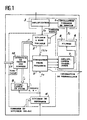
- the fractional division frequency synthesizer which is represented in FIG. 1 comprises a voltage-controlled oscillator 1 coupled by its output to a variable-rank loop divider circuit 2 through separator amplifiers 3. It also includes a divider of reference frequency 4, a phase-frequency comparator 5, a servo control device 6 composed of an amplifier circuit 7 and a loop filter 8, a phase storage circuit 9 and a management interface circuit 10.
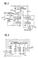
- the variable rank loop divider circuit 2 which is represented in FIG. 2 comprises a predivisor circuit 11 with two modulo Q / Q + 1 and two programmable synchronous counters 12 and 13 coupled to the output of the predivisor circuit 11.
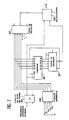
- the predivisor circuit 11 comprises, as shown in FIG. 3, a set of flip-flops mounted in a Johnson ring in which only Q + 1 states are kept to allow the realization of a divider with two modulo Q and Q + 1.
- the number of flip-flops is limited to 4 and flip-flops 14 and 16 form a ring with 8 possible states.
- a two-module 4/5 pre-divider is produced using flip-flops 14, 15 and 16.
- the flip-flop 17 makes it possible to carry out a double extension of the modulos, that is to say, to carry out a division by 8 or by 9.
- the signal to be divided provided by the output of the amplifiers (fig. 1) is applied to the clock inputs CK of flip-flops 14, 15 and 16 through two interface circuits 18 and 19 connected in series.
- the modulo Q or Q + 1 division mode is determined by the logic circuits "or" 20, 21 and 22 placed on the successive loops of the outputs of flip-flops 16, 15 and 14 on the input of flip-flop 14.
- the outputs of the predivisor 11 are selected by circuits "or" 24 and 25 controlled from an MS / SP control bit applied to the input of an inverter circuit 23.
- the output Q1 of the first flip-flop 14 constitutes the output signal of the predivisor and the output of the last flip-flop 17 is inhibited in this case.
- a timing diagram illustrating the operation of the predivisor is represented in FIG. 4. This represents the successive states of the outputs Q1 to Q4 of the flip-flops 14 to 17 as a function of the H states of the frequency signal F S supplied by the oscillator of FIG. 1 through amplifiers 3.
- the two counters 12 and 13 shown in FIG. 2 receive the clock signal H divided by Q or Q + 1 from the predivisor 11. These counters are programmed with the respective values N A and N P and count down simultaneously from these values , at the start of the division cycle by Q + 1, as long as the number N A has not been counted down to zero by the counter 12. When this occurs, the countdown of the counter 12 is stopped and the division rank of the predivisor 11 is positioned on Q by the output of a decoder 26 of the state "O" which controls the inhibition of the counter 12 (input E), and the loading of the division mode of the predivisor 11. At this instant there is (Q + 1) ⁇ N A clock pulses counted. The counting down of the number Np by the counter 13 continues until reaching the state "2" decoded by a decoder 27 formed by a "no or” gate or any equivalent device placed at the output of the counter 13.
- the decoding of state 2 constitutes information at the end of the division cycle. This is synchronized on the rising edge of the output clock of the predivisor 11 and controls the reloading of the counters 12 and 13 via a flip-flop 28, in synchronism with this clock, at the initial values N A and N P.
- the counter 12 is released, the predivisor 11 is positioned to divide by Q + 1 and the cycle begins again.
- the total number of H input clock overruns counted during a division cycle is:
- N (Q + 1) ⁇ N A + (N p - N A )
- the reference divider 4 makes it possible to obtain a reference frequency F R of the loop, submultiple of the external reference frequency. Its division rank is programmed by a 5-bit control word R ⁇ to R4.
- the divider of the reference frequency is constituted as shown in Figure 7 by a programmable 5-bit binary counter 30 which provides all the division ranges between 2 and 32 inclusive. This circuit counts down from the value programmed on its inputs D to the value "zero", in synchronism with the rising edge of a clock signal supplied by an external reference frequency).
- a decoding gate 31 disposed at the output of the counter 30 detects the state "0” and sends a level “0" on the "LOAD” input of counter 30, which authorizes its reloading at the value programmed on its D inputs.
- the reference frequency which is 12 MHz is obtained after dividing the external reference frequency 24 MHz by 2.
- the TACAN synthesizer loop reference frequency is 1 MHz; it is obtained after division by 24 of this same external reference frequency.
- the phase accumulator circuit 9 which is represented in FIG. 6 comprises a summing circuit 36 (3 bits) followed by a register 37 (4 bits) which makes it possible to synchronize on the rising edge of the clock, at the reference frequency F R , the information obtained at the output of the adder circuit 36 with the overflow signal C OUT of the register 37.
- the outputs (Q1 - Q3) of the register 37 are looped back to the inputs (B O - B2) of the adder circuit 36.
- phase accumulator circuit 9 determines at each reference cycle defined by the period of the signal supplied by the reference frequency divider 5 the mode of division by N or by N + 1 of the variable rank loop divider circuit .
- the module M of the phase accumulator circuit 4 is linked to the reference frequency F R and to the pitch P of the synthesizer by the relation:
- the content of register 37 is increased by the number F at each period 1 / F R of the reference signal.
- the accumulator circuit 37 When the content of register 37 reaches or exceeds the value M, the accumulator circuit 37 provides an overflow signal which is applied to the retaining input cin of the adder circuit 29 to control the incrementation of the division rank N of a unit . (command N, N + 1 in Figures 1 and 2).
- the successive values of the content P k of the accumulator register 37 correspond to the phase difference which exists between the loop signal F S / N and the reference frequency F R.
- the phase-frequency comparator circuit 5 measures the frequency difference between the output signal of the variable rank divider of frequency F S / N and the frequency reference signal F R during the transient loop servo period during d 'a change of frequency.
- the comparator circuit 5 When the loop is stabilized, the comparator circuit 5 provides, at each reference period 1 / F R, a measurement of the phase difference between the signals F S / N and F R.
- This circuit comprises two “D type” flip-flops, 38, 39 coupled to two multiplexer circuits 40, 41.
- the flip-flops 38, 39 are activated on the rising edge of the clock C p , and their Q outputs are looped back to the "Reset" inputs via a "no or” gate 42.
- the transfer characteristic of the comparator circuit 5 must be very linear in this range and without dead zone so as to maintain constant the gain of the phase comparator circuit 5 and therefore the gain of the phase loop.
- the multiplexers 40 and 41 with 2 inputs make it possible to swap the signals at the input of the comparator according to the control signal CPF. This device makes it possible to reverse the direction of control of oscillator 1.
- phase frequency comparator circuit 5 is usefully supplemented by a loop locking detection device shown in FIG. 10 where the elements of the comparator circuit 5 homologous to those of FIG. 8 are represented with the same references.
- This device provides reliable information to detect any malfunction of the synthesizer. For this it uses the signals "UP” and “DOWN” appearing at the output of the comparator circuit 5 and delivers a logic state “1" when the phase loop is locked, or a state "0" otherwise.
- phase-frequency comparator circuit 5 Depending on the situation of the phase loop, various signals may appear at the output of the phase-frequency comparator circuit 5. These different cases are summarized in the table in FIG. 11.
- the signals "UP” and “DOWN” at the output of the comparator circuit 5 are sent to the input of a "or exclusive” circuit 43. They are formed when the loop is not locked, either of a level “1” is a succession of "0" and “1” with a high proportion of "1".
- the output signal from the "OR” circuit 44 is applied to the reset input MR of a counter 45 which has the reference frequency FR as a clock.
- MR 1
- the outputs Q of the counter 45 which are combined at the input of a "NO OR” gate 46 deliver a state " 1 ".
- the counter 45 is reset frequently and has a permanent state "1" at the output of the "NO OR” circuit 46, since it does not have in this case time to finish counting. This state is reversed by the amplifier 47 before being transmitted to the output of the detection device.
- a filter 48 disposed at the output of the "or exclusive" circuit 43 makes it possible to smooth the parasitic pulses which may appear during the transitions of the equilibrium pulses.
- This filter consists of a capacitor CL.
- the loop reacts very quickly and the equilibrium pulses at the output of the phase comparator 5 are not sufficiently disturbed to be detected by this device; the "OR" circuit 44 applies to the input MR of the counter 45 a signal CHF2, coming from the data management interface 10.
- the CHF2 signal to trigger the counting and to indicate the unlocking of the loop during the control phase.
- the servo control device shown respectively for the TDMA and TACAN applications in FIGS. 13A and 13B, comprises a charge-pump amplifier 7, coupled to loop filters 48 and rejectors 49 and to a low-pass filter 50 connected serial.
- the charge-pump amplifier 7 consists of two switched current sources I UP and I DOWN , formed by transistors 50 to 57 which charge and discharge an integration capacitor 62.
- the two current sources comprise two symmetrical UP and DOWN channels each composed of a first differential pair of transistors 50, 51 respectively 52, 53 which performs a level translation to control a second pair 54, 55 respectively 56, 57 of transistors which performs the switching of the charge and / or discharge current of the integration capacity 62.
- the switching command is provided by the output signals "UP" and "DOWN” and their complement supplied by the comparator 5.
- the speed of the switches, each of which is constituted by a differential transistor stage allows to take into account the fine pulses at the output of the phase comparator 5.
- the conversion gain of the phase comparator and charge-pump amplifier 7 assembly is defined by the value of the output current which is optimized as a function of the loop gain and the desired response speed.
- the loop filter 48 formed by the resistor 60 and the capacitors 61 and 62 is determined so as to obtain the characteristics of phase noise and of acquisition time sought.
- a slow TACAN type synthesizer must be able to have a narrow loop bandwidth (cutoff frequency 30 KHz), and a fast TDMA type synthesizer must have a wide loop bandwidth (cutoff frequency 400 KHz).
- rejection filters 49 for the TACAN and 66 for the TDMA formed by series resonant elements centered, for example, on the frequency 12 MHz for the production of the TDMA and 1 MHz synthesizers for the production of TACAN synthesizers.
- the other harmonic lines of the reference frequency are filtered by the loop.
- the fractionation lines at multiple frequencies of 3 MHz are eliminated by means of filter filters 63, 64, 65 centered on the frequencies of 3 MHz, 6 MHz and 9 MHz.
- the other harmonic lines of 3 MH and of frequency higher than 12 MHz do not require specific filtering because they are already strongly attenuated by the loop filtering.
- the lines at 3 and 6 MHz which are closest to the loop bandwidth each require to be reduced to a level below -70 dB c two self L and capacitance rejectors (a 63 bis LC series plug circuit followed by '' a parallel LC circuit to attenuate the lines at 3 MHz and two parallel circuits 64, 64 bis to attenuate the lines at 6 MHz).
- the data management interface which is shown in FIG. 12 manages the synthesizer control information supplied by the radio bus CR of FIG. 1, for the specific operating modes of the TDMA and TACAN synthesizers.
- the control information of the TDMA synthesizer is composed of an 8-bit parallel word, 6 of which are used to define the number of the frequency channel (between 0 and 50) on which the synthesizer must operate.
- the information is taken into account on the rising edge of the pulse of the signal CHF1 which constitutes the clock of a register 67 validated by the low level of the signal ENABLE.
- the channel information CR is applied to an interface circuit 72 and is transformed into control information for the variable rank divider 2 (words N A on 3 bits and N p on 8 bits in this example for programming the counters 12 and 13 FIG. 2) and of the phase accumulator circuit 9 (word F over 3 bits) via a coding circuit 68 connected to the register 67.
- control information for a TACAN synthesizer is constituted in this example by two serial words of 8 parallel bits whose format is shown in FIGS. 15A and 15B.
- bits D0 to D4 forming the 2nd word can all have the value 0.
- the first 8-bit word is taken into account on the rising edge of the first pulse of the CHF1 signal by register 67 under the control of a gate 73.
- the second 8-bit word is taken into account on the rising edge of the second pulse of the CHF1 signal by a register 69 under the control of a door 74.
- a REGISTER SELECT signal combined with the ENABLE signal makes it possible to validate successively the registers 67 and 69.
- a buffer register 70 is validated at the same time as the register 69 in order to transfer to a 16-bit input of a multiplexer 71, the first 8-bit word simultaneously with the second word, on the rising edge of the second pulse of the CHF1 signal.
- the multiplexer 71 receives on its second 16-bit input, the TDMA information at the output of the coding circuit 68.
- This has the advantage of making it possible to select, from a wired TDMA / TACAN command, the control information synthesizer for TDMA mode or TACAN mode.
- the interface circuit also includes a 75 bis sequencer, which delivers a CHF2 signal to select the second pulse of the CHF1 signal in TACAN mode.
- the data management interface can operate, for example, with a clock frequency of 5 MHz.
- oscillator 1 For the TDMA application, oscillator 1 must be able to cover the 1242-1479 MHz frequency band while maintaining a very linear voltage-frequency transfer characteristic to maintain a constant loop gain and spectral purity performance of the synthesizer throughout the frequency range.
- the oscillator For a TACAN synthesizer, the oscillator must be able to cover the transmit and receive frequency bands from 1025 to 1474 MHz.
- the frequency range covered by this oscillator is therefore greater than that covered by the oscillator of the TDMA application, but in this case it is not necessary to have such a high linearity because the preservation of the purity performances spectral in the frequency range is less critical. It is thus possible to obtain, whatever the applications, a floor noise lower than -150 dBc / Hz from a frequency deviation of ⁇ 10% of the central frequency and an output level of the oscillator of +13 dBm.
Abstract
Description
La présente invention concerne un synthétiseur hyperfréquence à division fractionnaire.The present invention relates to a fractional division microwave synthesizer.
Elle s'applique notamment à la réalisation de synthétiseurs pour les systèmes de radiocommunication à haut débit de transmission, connus sous les désignations anglo-saxonnes TDMA et TACAN, où TDMA est l'abréviation de "Time division multiple access" et TACAN est l'abréviation de "Tactical Air Navigation".It applies in particular to the production of synthesizers for high-speed transmission radio systems, known under the English designations TDMA and TACAN, where TDMA is the abbreviation for "Time division multiple access" and TACAN is the abbreviation for "Tactical Air Navigation".
Typiquement les synthétiseurs TDMA sont des synthétiseurs à temps d'acquisition très court de 15 µs au pas de 3 MHz, qui sont utilisés pour l'émission et la réception d'informations dans la bande de fréquence 1242 à 1479 MHz. Par contre, les synthétiseurs TACAN sont des synthétiseurs à temps d'acquisition lent de 1 ms au pas de 1 MHz, qui sont utilisés pour l'émission d'informations dans la bande de fréquence 1025 à 1150 MHz et pour la réception d'informations dans la bande 1223 à 1474 MHz.Typically TDMA synthesizers are synthesizers with a very short acquisition time of 15 µs in steps of 3 MHz, which are used for the transmission and reception of information in the frequency band 1242 to 1479 MHz. On the other hand, TACAN synthesizers are synthesizers with a slow acquisition time of 1 ms in steps of 1 MHz, which are used for transmitting information in the frequency band 1025 to 1150 MHz and for receiving information in the band 1223 to 1474 MHz.
Dans les synthétiseurs de fréquence à division fractionnaire connus, le rang de division n'est pas fixe mais varie entre les rangs N et N + 1 selon une loi calculée en temps réel, ce qui permet d'obtenir un pas élémentaire de fréquence sous-multiple de la fréquence de référence. Cette division s'effectue généralement en considérant M périodes de référence, durant lesquelles il y a F divisions par N + 1 et (M - F) divisions par N. On obtient de la sorte un rang de division moyen Nm tel que:![]()
![]()
La fréquence synthétisée FS s'écrit alors en fonction de la fréquence de référence FR:![]()
![]()
Ce principe de synthèse introduit au niveau du comparateur de phase du synthétiseur, une erreur de phase cyclique provoquant une modulation de fréquence de l'oscillateur contrôlé en tension, et la fréquence de modulation est égale au décalage de fréquence fractionnaire. Cette modulation est annulée habituellement au moyen d'un dispositif de compensation actif qui corrige l'erreur de phase. Cependant ce dispositif n'est pas applicable aux synthétiseurs des applications TDMA car s'il permet d'atténuer fortement les raies de fractionnement, il n'est pas compatible du temps d'acquisition recherché. En effet, si le temps de commutation reste acceptable pour un petit saut de fréquence il ne l'est plus pour les sauts plus importants. Cela est dû essentiellement aux saturations successives qui se produisent dans l'amplificateur intégrateur de boucle durant la phase d'asservissement.This synthesis principle introduces at the level of the phase comparator of the synthesizer, a cyclic phase error causing a frequency modulation of the voltage controlled oscillator, and the modulation frequency is equal to the offset fractional frequency. This modulation is usually canceled by means of an active compensation device which corrects the phase error. However, this device is not applicable to synthesizers of TDMA applications because if it makes it possible to greatly attenuate the fractionation lines, it is not compatible with the acquisition time sought. Indeed, if the switching time remains acceptable for a small frequency jump it is no longer acceptable for larger jumps. This is mainly due to the successive saturations that occur in the loop integrator amplifier during the servo phase.
C'est pourquoi les solutions connues mises en oeuvre pour réaliser ces synthétiseurs font généralement appel aux techniques de synthèse de fréquence directe ou indirecte.This is why the known solutions used to produce these synthesizers generally use direct or indirect frequency synthesis techniques.
Un exemple connu de technique de synthèse de fréquence directe qui est dans son principe basée sur la commutation de 4 oscillateurs asservis, dont les fréquences sont additionnées et divisées répétitivement de façon à obtenir le pas recherché, permet d'obtenir un temps de commutation des fréquences utilisées très inférieur à 15 µs. Cependant, cette technique impose l'utilisation de composants coûteux et volumineux pour la réalisation des circuits mélangeurs et diviseurs de fréquence ainsi que celle des filtres successifs et les nombreuses raies parasites qui sont générées par ce type de réalisation ne conduisent pas à retenir cette solution. Pour les mêmes raisons le principe de synthèse directe à sélection et mélange d'harmoniques connu utilisant des filtres à onde de surface SAW ne peut non plus être adopté.A known example of a direct frequency synthesis technique which is in principle based on the switching of 4 slave oscillators, the frequencies of which are added and divided repeatedly so as to obtain the desired pitch, makes it possible to obtain a frequency switching time. used much less than 15 µs. However, this technique requires the use of expensive and bulky components for the production of mixer circuits and frequency dividers as well as that of successive filters and the numerous parasitic lines which are generated by this type of construction do not lead to this solution being adopted. For the same reasons, the known principle of direct synthesis with selection and mixing of harmonics using SAW surface wave filters cannot be adopted either.
Dans la technique de la synthèse indirecte un principe de synthèse connu à deux boucles à verrouillage de phase, utilisant une boucle "pas gros" et une boucle "pas fin" avec prépositionnement d'oscillateur ainsi qu'un oscillateur de transposition permet théoriquement d'obtenir le temps d'acquisition recherché mais il conduit à un synthétiseur trop volumineux et trop consommant pour les applications envisagées.In the technique of indirect synthesis, a known synthesis principle with two phase-locked loops, using a "not large" loop and a "not fine" loop with oscillator prepositioning as well as a transposition oscillator theoretically allows obtain the desired acquisition time, but it leads to a synthesizer that is too bulky and too consuming for the applications envisaged.
Le but de l'invention est de pallier les inconvénients précités.The object of the invention is to overcome the aforementioned drawbacks.
A cet effet, l'invention a pour objet, un synthétiseur hyperfréquence à division fractionnaire du type comprenant un oscillateur commandé en tension couplé à une première entrée d'un comparateur phase-fréquence par l'intermédiaire d'un diviseur de fréquence à rang variable pour comparer la fréquence et la phase du signal fourni par la sortie du diviseur de fréquence à rang variable à la fréquence et à la phase d'un signal de référence appliqué sur une deuxième entrée du comparateur phase fréquence, un dispositif de commande pour asservir la fréquence d'oscillation de l'oscillateur commandé en tension sur une fréquence multiple entier et/ou fractionnaire de la fréquence FR du signal de référence en fonction du rang de division du diviseur de fréquence à rang variable et un circuit accumulateur de phase pour commander le rang de division du diviseur de fréquence à rang variable caractérisé en ce que le circuit comparateur de phase délivre respectivement sur une première sortie UP une première suite et sur une deuxième sortie DOWN une deuxième suite d'impulsions en fonction respectivement de l'avance ou du retard de phase des signaux appliqués sur sa première et sa deuxième entrée, les deux suites d'impulsions étant délivrées simultanément, en phase l'une avec l'autre, de même largeur et en phase avec le signal de référence lorsque les signaux appliqués sur les première et deuxième entrées du comparateur sont en phase et en ce que le dispositif de commande d'asservissement comprend une capacité d'intégration chargée et déchargée respectivement par les impulsions de l'une ou de l'autre suite, pour fournir en fonction de la tension développée aux bornes de la capacité un signal de commande d'avance ou de retard en fréquence et en phase de l'oscillateur.To this end, the subject of the invention is a fractional division microwave synthesizer of the type comprising a voltage-controlled oscillator coupled to a first input of a phase-frequency comparator via a frequency divider with variable rank to compare the frequency and the phase of the signal supplied by the output of the frequency divider with variable rank to the frequency and to the phase of a reference signal applied to a second input of the phase frequency comparator, a control device for controlling the oscillation frequency of the voltage-controlled oscillator on an integral multiple and / or fractional of the frequency F R of the reference signal as a function of the division rank of the frequency divider with variable rank and a phase accumulator circuit for controlling the division rank of the variable-rank frequency divider characterized in that the phase comparator circuit delivers respectively ent on a first output UP a first sequence and on a second output DOWN a second sequence of pulses as a function respectively of the advance or of the phase delay of the signals applied to its first and its second input, the two sequences of pulses being delivered simultaneously, in phase with one another, of the same width and in phase with the reference signal when the signals applied to the first and second comparator inputs are in phase and in that the control device slaving comprises an integration capacity charged and discharged respectively by the pulses of one or the other sequence, to supply as a function of the voltage developed at the terminals of the capacity a frequency advance or delay control signal and in phase of the oscillator.
L'invention a pour avantage qu'elle permet de réaliser un synthétiseur ne comportant qu'une seule boucle à verrouillage de phase qui possède de ce fait un encombrement réduit, et dans lequel le choix de la fréquence de référence qui détermine la rapidité d'acquisition est indépendant du pas de fréquence. D'autre part, l'architecture obtenue se prête à la miniaturisation du synthétiseur car elle permet d'intégrer toutes les fonctions logiques sur un même substrat en mettant en oeuvre une technologie ECL peu consommante d'énergie et en hybridant les parties analogiques.The invention has the advantage that it makes it possible to produce a synthesizer comprising only a single phase locked loop which therefore has a reduced bulk, and in which the choice of the reference frequency which determines the acquisition speed is independent of the frequency step. On the other hand, the architecture obtained lends itself to the miniaturization of the synthesizer because it makes it possible to integrate all the logic functions on the same substrate by implementing an ECL technology that consumes little energy and by hybridizing the analog parts.
Enfin, l'utilisation d'un réseau de circuits réjecteurs passifs à la sortie du comparateur de phase, et d'un diviseur fractionnaire à rang de division faible permet de remplacer efficacement le dispositif de compensation utilisé habituellement pour corriger l'erreur de phase inhérente au principe de la division fractionnaire qui provoque une modulation de fréquence de l'oscillateur commandé en tension.Finally, the use of a network of passive rejector circuits at the output of the phase comparator, and of a fractional divider with a low division rank makes it possible to effectively replace the compensation device usually used to correct the inherent phase error. to the principle of fractional division which causes a frequency modulation of the voltage controlled oscillator.
D'autres caractéristiques et avantages de l'invention apparaîtront ci-après à l'aide de la description qui suit faite en regard des dessins annexés qui représentent:
- la figure 1, un schéma synoptique d'un synthétiseur selon l'invention;
- la figure 2, un mode de réalisation du diviseur à rang variable de la figure 1;
- la figure 3, un mode de réalisation du prédiviseur de la figure 2;
- la figure 4, un diagramme de temps représentant le fonctionnement du prédiviseur de la figure 3;
- la figure 5, un diagramme de temps représentant le fonctionnement du diviseur à rang variable de la figure 2;
- la figure 6, un mode de réalisation de l'accumulateur de phase de la figure 1;
- la figure 7, un mode de réalisation du diviseur de référence de la figure 1;
- la figure 8, un mode de réalisation du comparateur phase fréquence de la figure 1;
- les figures 9A et 9B, deux graphes des temps illustrant le fonctionnement du comparateur phase fréquence de la figure 8.
- la figure 10, un mode de réalisation d'un dispositif de détection de verrouillage de phase;
- la figure 11, un tableau pour illustrer le fonctionnement du dispositif de la figure 10;
- la figure 12, un mode de réalisation de l'interface de gestion des données du synthétiseur représenté à la figure 1;
- les figures 13A et 13B, deux modes de réalisation de l'amplificateur charge-pompe et du filtre de boucle de la figure 1;
- la figure 14, le couplage des amplificateurs de sortie et de boucle du synthétiseur à la sortie de l'oscillateur commandé en tension de la figure 1;
- les figures 15A et 15B les formats des mots de commande du synthétiseur.
- Figure 1, a block diagram of a synthesizer according to the invention;
- Figure 2, an embodiment of the variable row divider of Figure 1;
- Figure 3, an embodiment of the predivisor of Figure 2;
- FIG. 4, a time diagram representing the operation of the predivisor of FIG. 3;
- FIG. 5, a time diagram representing the operation of the variable rank divider of FIG. 2;
- Figure 6, an embodiment of the phase accumulator of Figure 1;
- Figure 7, an embodiment of the reference divider of Figure 1;
- Figure 8, an embodiment of the phase frequency comparator of Figure 1;
- FIGS. 9A and 9B, two time graphs illustrating the operation of the phase frequency comparator of FIG. 8.
- FIG. 10, an embodiment of a phase lock detection device;
- Figure 11, a table to illustrate the operation of the device of Figure 10;
- Figure 12, an embodiment of the data management interface of the synthesizer shown in Figure 1;
- Figures 13A and 13B, two embodiments of the charge pump amplifier and the loop filter of Figure 1;
- FIG. 14, the coupling of the output and loop amplifiers of the synthesizer to the output of the voltage controlled oscillator of FIG. 1;
- FIGS. 15A and 15B the formats of the control words of the synthesizer.
Le synthétiseur de fréquence à division fractionnaire qui est représenté à la figure 1 comprend, un oscillateur commandé en tension 1 couplé par sa sortie à un circuit diviseur de boucle à rang variable 2 au travers d'amplificateurs séparateurs 3. Il comprend également un diviseur de fréquence de référence 4, un comparateur phase-fréquence 5, un dispositif de commande d'asservissement 6 composé d'un circuit amplificateur 7 et d'un filtre de boucle 8, un circuit accumulateur de phase 9 et un circuit d'interface de gestion de données 10.The fractional division frequency synthesizer which is represented in FIG. 1 comprises a voltage-controlled
Le circuit diviseur de boucle à rang variable 2 qui est représenté à la figure 2 comprend, un circuit prédiviseur 11 à deux modulo Q/Q + 1 et deux compteurs synchrones programmables 12 et 13 couplé à la sortie du circuit prédiviseur 11. Le circuit prédiviseur 11 comporte de la façon représentée à la figure 3, un ensemble de bascules montées en anneau de Johnson dans lesquelles seuls Q + 1 états sont conservés pour permettre la réalisation d'un diviseur à deux modulo Q et Q + 1.The variable rank
Dans l'exemple de la figure 3, le nombre des bascules est limité à 4 et les bascules 14 et 16 forment un anneau à 8 états possibles. Un prédiviseur à deux modules 4/5 est réalisé à l'aide des bascules 14, 15 et 16.In the example in FIG. 3, the number of flip-flops is limited to 4 and flip-
La bascule 17 permet d'effectuer une extension double des modulo, c'est-à-dire, de réaliser une division par 8 ou par 9.The flip-
Le signal à diviser fourni par la sortie des amplificateurs (fig. 1) est appliqué sur les entrées d'horloge CK des bascules 14, 15 et 16 au travers de deux circuits d'interface 18 et 19 montés en série. Le mode de division modulo Q ou Q + 1 est déterminé par les circuits logiques "ou" 20, 21 et 22 placés sur les rebouclages successifs des sorties des bascules 16, 15 et 14 sur l'entrée de la bascule 14.The signal to be divided provided by the output of the amplifiers (fig. 1) is applied to the clock inputs CK of flip-
Les sorties du prédiviseur 11 sont sélectionnées par des circuits "ou" 24 et 25 commandés à partir d'un bit de commande MS/SP appliqué sur l'entrée d'un circuit inverseur 23. Ainsi, en mode de division 4/5 la sortie Q₁ de la première bascule 14 constitue le signal de sortie du prédiviseur et la sortie de la dernière bascule 17 est inhibée dans ce cas. Un chronogramme illustrant le fonctionnement du prédiviseur est représenté à la figure 4. Celui-ci représente les états successifs des sorties Q₁ à Q₄ des bascules 14 à 17 en fonction des états H du signal de fréquence FS fourni par l'oscillateur de la figure 1 au travers des amplificateurs 3.The outputs of the
Les deux compteurs 12 et 13 représentés sur la figure 2 reçoivent le signal d'horloge H divisé par Q ou Q + 1 issu du prédiviseur 11. Ces compteurs sont programmés aux valeurs respectives NA et NP et décomptent simultanément à partir de ces valeurs, au début du cycle de division par Q + 1, tant que le nombre NA n'a pas été décompté à zéro par le compteur 12. Lorsque cela se produit, le décomptage du compteur 12 est arrêté et le rang de division du prédiviseur 11 est positionné sur Q par la sortie d'un décodeur 26 de l'état "O" qui commande l'inhibition du compteur 12 (entrée E), et le chargement du mode de division du prédiviseur 11. A cet instant il y a (Q + 1) × NA impulsions d'horloge comptées. Le décomptage du nombre Np par le compteur 13 se poursuit jusqu'à atteindre l'état "2" décodé par un décodeur 27 formé par une porte "non ou "ou tout dispositif équivalent placé à la sortie du compteur 13.The two
Le décodage de l'état 2 constitue une information de fin de cycle de division. Celle-ci est synchronisée sur le front montant de l'horloge de sortie du prédiviseur 11 et commande le rechargement des compteurs 12 et 13 par l'intermédiaire d'une bascule 28, en synchronisme avec cette horloge, aux valeurs initiales NA et NP. Le compteur 12 se débloque, le prédiviseur 11 est positionné pour diviser par Q + 1 et le cycle recommence. Le nombre total d'implusions d'horloge d'entré H comptées au cours d'un cycle de division est:The decoding of
N = (Q + 1) × NA + (Np - NA)Q = QNp + NA
en mode 8/9 on obtient N = 8Np + NA et en mode 4/5 on obtient N = 4Np + NA N = (Q + 1) × N A + (N p - N A ) Q = QN p + N A
in 8/9 mode we get N = 8N p + N A and in 4/5 mode we get N = 4N p + N A
Pour que le fonctionnement soit possible et s'effectue sans ambiguïté il faut que la relation:For the operation to be possible and to be carried out without ambiguity, the relationship must:
Np - NA > 0 soit vérifiée, d'où Npmin = NAmax. Avec par exemple, 0 ≦ NA ≦ 7, la valeur minimale que peut prendre N est alors:
Nmin = 8Npmin + NAmin = 56
Si le prédiviseur 11 est utilisé en mode 4/5 on aurait
pour 0 ≦ NA ≦ 3, Nmin = 12N p - N A > 0 is verified, hence N p min = N A max. For example, with 0 ≦ N A ≦ 7, the minimum value that N can take is then:
Nmin = 8N p min + N A min = 56
If the
for 0 ≦ N A ≦ 3, Nmin = 12
Un mode de séquencement des états pour un cycle de division correspondant à N = 119 et montré à la figure 5.A state sequencing mode for a division cycle corresponding to N = 119 and shown in Figure 5.
Le diviseur de référence 4 permet d'obtenir une fréquence de référence FR de la boucle, sous-multiple de la fréquence de référence externe. Son rang de division est programmé par un mot de commande de 5 bits R∅ à R4.The
Le diviseur de la fréquence de référence est constitué de la manière représentée à la figure 7 par un compteur binaire 5-bit programmable 30 qui fournit tous les rangs de division compris entre 2 et 32 inclus. Ce circuit décompte de la valeur programmée sur ses entrées D jusqu'à la valeur "zéro", en synchronisme avec le front montant d'un signal d'horloge fourni par une fréquence de référence externe). Une porte de décodage 31 disposée en sortie du compteur 30 détecte l'état "0" et envoie un niveau "0" sur l'entrée "LOAD" du compteur 30 ce qui, autorise son rechargement à la valeur programmée sur ses entrées D.The divider of the reference frequency is constituted as shown in Figure 7 by a programmable 5-bit
Lorsque la commande R du rang de division du diviseur de référence 4 est égale à "0", cet état est détecté par une porte de décodage 32 au travers d'un circuit d'interface 34 qui envoie un signal de commande permettant de sélectionner la voie Do d'un multiplexeur à 2 entrées. Le signal "référence externe" est appliqué sur l'entrée Do d'un multiplexeur 33 au travers d'un circuit de mise en forme 35 et le signal de sortie du compteur 30 sur l'entrée D1 de ce même multiplexeur 33 au travers de la porte de décodage 31.When the command R of the division rank of the
Ce dispositif permet lorsque le rang de division est nul (R = 0) d'avoir une fréquence de référence de boucle FR égale à la fréquence de référence externe.This device allows when the division rank is zero (R = 0) to have a reference frequency of loop FR equal to the external reference frequency.
Pour le synthétiseur TDMA la fréquence de référence qui est de 12 MHz est obtenue après division par 2 de la fréquence de référence externe 24 MHz. La fréquence de référence de boucle du synthétiseur TACAN est de 1 MHz; elle est obtenue après division par 24 de cette même fréquence de référence externe.For the TDMA synthesizer, the reference frequency which is 12 MHz is obtained after dividing the
Le circuit accumulateur de phase 9 qui est représenté à la figure 6 comprend un circuit additonneur 36 (3 bits) suivi d'une registre 37 (4 bits) qui permet de synchroniser sur le front montant de l'horloge, à la fréquence de référence FR, les informations obtenues en sortie du circuit additionneur 36 avec le signal de débordement COUT du registre 37. Les sorties (Q₁ - Q₃) du registre 37 sont rebouclées sur les entrées (BO - B₂) du circuit additionneur 36.The
Le rôle du circuit accumulateur de phase 9 est de déterminer à chaque cycle de référence défini par la période du signal fourni par le diviseur de fréquence de référence 5 le mode de division par N ou par N + 1 du circuit diviseur de boucle à rang variable.The role of the
Le module M du circuit accumulateur de phase 4 est lié à la fréquence de référence FR et au pas P du synthétiseur par la relation:The module M of the
M = FR/PM = F R / P
Les informations de commande en fréquence du synthétiseur sont fournies par le rang de division N utilisé lors de la programmation du diviseur à rang variable 2 et par le terme fractionnaire F appliqué à l'entrée du circuit accumulateur de phase 4 qui est défini suivant la relation (2) par la relation:![]()
![]()
Le contenu du registre 37 est augmenté du nombre F à chaque période 1/FR du signal de référence.The content of
Le contenu Pk du registre de l'accumulateur 37 est de la sorte égal, à la Kième période d'horloge à Pk = (Pk-1 + F) modulo M (5).The content P k of the
La valeur maximale de Pk étant M - 1.The maximum value of P k being M - 1.
Lorsque le contenu du registre 37 atteint ou dépasse la valeur M, le circuit accumulateur 37 fournit un signal de débordement qui est appliqué sur l'entrée de retenue cin du circuit additionneur 29 pour commander l'incrémentation du rang de division N d'une unité. (commande N,N + 1 sur les figures 1 et 2).When the content of
Les valeurs successives du contenu Pk du registre accumulateur 37 correspondent à la diférence de phase qui existe entre le signal de boucle FS/N et la fréquence de référence FR.The successive values of the content P k of the
Le circuit comparateur phase-fréquence 5 mesure l'écart de fréquence entre le signal de sortie du diviseur à rang variable de fréquence FS/N et le signal de référence de fréquence FR pendant la période transitoire d'asservissement de la boucle lors d'un changement de fréquence.The phase-
Lorsque la boucle est stabilisée le circuit comparateur 5 fournit à chaque période de référence 1/FR une mesure de l'écart de phase entre les signaux FS/N et FR.When the loop is stabilized, the
Ce circuit comprend deux bascules de "type D", 38, 39 couplées à deux circuits multiplexeurs 40, 41. Les bascules 38, 39 sont activées sur le front montant de l'horloge Cp, et leurs sorties Q sont rebouclées sur les entrées "Reset" par l'intermédiaire d'une porte "non ou" 42.This circuit comprises two “D type” flip-flops, 38, 39 coupled to two
Pendant la phase transitoire d'asservissement de la boucle il n'y a plus aucune relation de phase entre les signaux à l'entrée du comparateur 5, les sorties Q des bascules 38 et 39 délivrent respectivement une information d'avance "UP" ou de retard de phase "DOWN" d'un signal par rapport à l'autre.During the transient loop servo-phase there is no longer any phase relationship between the signals at the input of
Lorsque la boucle est stabilisée, les signaux de sortie "UP", "DOWN" du comparateur 5 sont constitués par une suite d'implusions très fines de période égale à celle du signal de référence appliqué à l'entrée du comparateur. Ces impulsions en sorties "UP" et "DOWN" sont en phase. Des graphes du fonctionnement correspondant du circuit comparateur sont représentés aux figures 9A et 9B.When the loop is stabilized, the output signals "UP", "DOWN" of the
Comme les performances du synthétiseur, notamment en ce qui concerne sa pureté spectrale, sont mesurées lorsque la boucle est verrouillée, c'est-à-dire, lorsque le comparateur fonctionne au voisinage de l'écart de phase nul, la caractéristique de transfert du circuit comparateur 5 doit être très linéaire dans cette plage et sans zone morte de façon à maintenir constant le gain du circuit comparateur de phase 5 et donc le gain de la boucle de phase.As the performance of the synthesizer, in particular with regard to its spectral purity, is measured when the loop is locked, that is to say, when the comparator operates in the vicinity of the zero phase difference, the transfer characteristic of the
Les multiplexeurs 40 et 41 à 2 entrées permettent de permuter les signaux à l'entrée du comparateur en fonction du signal de commande CPF. Ce dispositif permet d'inverser le sens de commande de l'oscillateur 1.The
Le circuit comparateur phase fréquence 5 est complété utilement par un dispositif de détection à verrouillage de boucle représenté à la figure 10 où les éléments du circuit comparateur 5 homologues à ceux de la figure 8 sont représentés avec le mêmes références.The phase
Ce dispositif fournit une information fiable permettant de détecter tout mauvais fonctionnement du synthétiseur. Pour cela il exploite les signaux "UP" et "DOWN" apparaissant en sortie du circuit comparateur 5 et délivre un état logique "1" lorsque la boucle de phase est verrouillée, ou un état "0" dans le cas contraire.This device provides reliable information to detect any malfunction of the synthesizer. For this it uses the signals "UP" and "DOWN" appearing at the output of the
En fonction de la situation de la boucle de phase différents signaux peuvent apparaître en sortie du circuit comparateur phase-fréquence 5. Ces différents cas sont résumés dans le tableau de la figure 11.Depending on the situation of the phase loop, various signals may appear at the output of the phase-
Sur la figure 10 les signaux "UP" et "DOWN" en sortie du circuit comparateur 5 sont envoyés à l'entrée d'un circuit "ou exclusif" 43. Ils sont constitués lorsque la boucle n'est pas verrouillée, soit d'un niveau "1" soit d'une succession de "0" et de "1" avec une forte proportion de "1". Le signal de sortie du circuit "OU" 44 est appliqué à l'entrée MR de remise à zéro d'un compteur 45 qui a pour horloge la fréquence de référence FR. Lorsque la sortie du circuit "OU" 44 est dans l'état "1" permanent (MR = 1), les sorties Q du compteur 45 qui sont réunies à l'entrée d'une porte "NON OU" 46 délivrent un état "1".In FIG. 10, the signals "UP" and "DOWN" at the output of the
S'il s'agit d'une succession d'états "1", le compteur 45 est réinitialisé fréquemment et présente en sortie du circuit "NON OU" 46 un état "1" permanent, car il n'a pas dans ce cas le temps de terminer son comptage. Cet état est inversé par l'amplificateur 47 avant d'être transmis à la sortie du dispositif de détection.If it is a succession of states "1", the
Lorsque la boucle est verrouillée, les impulsions d'équilibre présentes sur les sorties Q du compteur 45 sont en phase et l'entrée MR du compteur 45 passe à l'état "0". Un filtre 48 disposé en sortie du circuit "ou exclusif" 43 permet de lisser les impulsions parasites pouvant apparaître lors des transitions des impulsions d'équilibre. Ce filtre est constitué par un condensateur CL. Lorsque l'entrée MR = 0 le compteur 45 compte 15 périodes d'horloge de référence. En fin de comptage, il fournit un état "0" en sortie du circuit "non ou" 46 qui réunit les sorties Q du compteur 45, ce qui bloque le comptage (du fait du rebouclage sur l'entrée d'inhibition d'horloge
Comme pour un saut de fréquence de faible amplitude (1 à 2 pas de fréquence par exemple), la boucle réagit très vite et les impulsions d'équilibre en sortie du comparateur de phase 5 ne sont pas suffisamment perturbées pour être détectées par ce dispositif; le circuit "OU" 44 applique à l'entrée MR du compteur 45 un signal CHF₂, provenant de l'interface de gestion des données 10.As for a low amplitude frequency jump (1 to 2 frequency steps for example), the loop reacts very quickly and the equilibrium pulses at the output of the
Le signal CHF₂ de déclencher le comptage et d'indiquer le déverrouillage de la boucle lors de la phase d'asservissement.The CHF₂ signal to trigger the counting and to indicate the unlocking of the loop during the control phase.
Le dispositif de commande d'asservissement, représenté respectivement pour les applications TDMA et TACAN aux figures 13A et 13B, comprend, un amplificateur charge-pompe 7, couplé à des filtres de boucle 48 et réjecteurs 49 et à un filtre passe-bas 50 reliés en série.The servo control device, shown respectively for the TDMA and TACAN applications in FIGS. 13A and 13B, comprises a charge-
L'amplificateur charge-pompe 7 est constitué par deux sources de courant IUP et IDOWN commutées, formées des transistors 50 à 57 qui chargent et déchargent une capacité d'intégration 62. Les deux sources de courant comportent deux voies UP et DOWN symétriques composées chacune d'une première paire différentielle de transistors 50, 51 respectivement 52, 53 qui effectue une translation de niveau pour commander une deuxième paire 54, 55 respectivement 56, 57 de transistors qui effectue la commutation du courant de charge et/ou de décharge de la capacité d'intégration 62. La commande de commutation est assurée par les signaux de sortie "UP" et "DOWN" et leur complément fournis par le comparateur 5. La rapidité des commutateurs dont chacun est constitué par un étage différentiel à transistors permet de prendre en compte les impulsions fines en sortie du comparateur de phase 5.The charge-
Le gain de conversion de l'ensemble comparateur de phase et amplificateur charge-pompe 7 est défini par la valeur du courant de sortie qui est optimisé en fonction du gain de boucle et de la rapidité de réponse recherchée.The conversion gain of the phase comparator and charge-
Le filtre de boucle 48 formé de la résistance 60 et des capacités 61 et 62 est déterminé de façon à obtenir les caractéristiques de bruit de phase et de temps d'acquisition recherchées.The
A titre d'exemple, un synthétiseur lent type TACAN doit pouvoir disposer d'une bande passante de boucle étroite (fréquence de coupure 30 KHz), et un synthétiseur rapide type TDMA doit disposer d'une bande passante de boucle large (fréquence de coupure 400 KHz).For example, a slow TACAN type synthesizer must be able to have a narrow loop bandwidth (
Les raies parasites multiples de la fréquence de référence sont éliminées au moyen de filtres réjecteurs 49 pour le TACAN et 66 pour le TDMA formés par des éléments résonnants séries centrés, par exemple, sur la fréquence 12 MHz pour la réalisation des synthétiseurs TDMA et 1 MHz pour la réalisation de synthétiseurs TACAN.The multiple parasitic lines of the reference frequency are eliminated by means of rejection filters 49 for the TACAN and 66 for the TDMA formed by series resonant elements centered, for example, on the
Les autres raies harmoniques de la fréquence de référence sont filtrées par la boucle.The other harmonic lines of the reference frequency are filtered by the loop.
Pour le synthétiseur TDMA, les raies de fractionnement aux fréquences multiples de 3 MHz sont éliminées au moyen de filtres réjecteurs 63, 64, 65 centrés sur les fréquences de 3 MHz, 6 MHz et 9 MHz. Les autres raies harmoniques de 3 MH et de fréquence supérieure à 12 MHz ne nécessitent pas de filtrage spécifique car elles sont déjà fortement atténuées par le filtrage de boucle.For the TDMA synthesizer, the fractionation lines at multiple frequencies of 3 MHz are eliminated by means of filter filters 63, 64, 65 centered on the frequencies of 3 MHz, 6 MHz and 9 MHz. The other harmonic lines of 3 MH and of frequency higher than 12 MHz do not require specific filtering because they are already strongly attenuated by the loop filtering.
Les raies à 3 et 6 MHz qui sont les plus proches de la bande passante de boucle nécessitent chacune pour être ramenée à un niveau inférieur à -70 dBc deux réjecteurs à self L et capacité C (un circuit bouchon 63 bis LC série suivi d'un circuit LC parallèle pour atténuer les raies à 3 MHz et deux circuits paralléle 64, 64 bis pour atténuer les raies à 6 MHz).The lines at 3 and 6 MHz which are closest to the loop bandwidth each require to be reduced to a level below -70 dB c two self L and capacitance rejectors (a 63 bis LC series plug circuit followed by '' a parallel LC circuit to attenuate the lines at 3 MHz and two
Deux circuits LC parallèles centrés à 9 MHz et 12 MHz permettent d'atténuer les raies à ces fréquences.Two parallel LC circuits centered at 9 MHz and 12 MHz make it possible to attenuate the lines at these frequencies.
L'interface de gestion de données qui est représentée à la figure 12, gère les informations de commande du synthétiseur fournies par le bus radio CR de la figure 1, pour les modes de fonctionnement spécifique des synthétiseurs TDMA et TACAN. Dans cet exemple, l'information de commande du synthétiseur TDMA est composé d'un mot de 8 bits parallèle dont 6 sont utilisés pour définir le numéro du canal de fréquence (compris entre 0 et 50) sur lequel doit fonctionner le synthétiseur.The data management interface which is shown in FIG. 12 manages the synthesizer control information supplied by the radio bus CR of FIG. 1, for the specific operating modes of the TDMA and TACAN synthesizers. In this example, the control information of the TDMA synthesizer is composed of an 8-bit parallel word, 6 of which are used to define the number of the frequency channel (between 0 and 50) on which the synthesizer must operate.
Les informations sont prises en compte sur le front montant de l'impulsion du signal CHF₁ qui constitue l'horloge d'un registre 67 validé par le niveau bas du signal ENABLE.The information is taken into account on the rising edge of the pulse of the signal CHF₁ which constitutes the clock of a
L'information de canal CR est appliquée sur un circuit d'interface 72 et est transformée en information de commande du diviseur à rang variable 2 (mots NA sur 3 bits et Np sur 8 bits dans cet exemple pour la programmation des compteurs 12 et 13 figure 2) et du circuit accumulateur de phase 9 (mot F sur 3 bits) par l'intermédiaire d'un circuit de codage 68 relié au registre 67.The channel information CR is applied to an
De même l'information de commande d'un synthétiseur TACAN est constituée dans cet exemple par deux mots série de 8 bits parallèles dont le format est représenté aux figures 15A et 15B.Similarly, the control information for a TACAN synthesizer is constituted in this example by two serial words of 8 parallel bits whose format is shown in FIGS. 15A and 15B.
Les informations contenues dans ces deux mots permettent de commander directement le diviseur à rang variable 2 (mots NA et Np respectivement sur 3 et 8 bits pour la programmation des compteurs 12 et 13), du circuit accumulateur de phase 9 (mot F sur 3 bits) et la permutation des entrées du comparateur de phase (mot CPF sur 1 bit).The information contained in these two words makes it possible to directly control the divider with variable rank 2 (words N A and N p respectively on 3 and 8 bits for the programming of
En mode TACAN les bits D0 à D4 formant le 2ème mot pourront tous avoir la valeur 0.In TACAN mode the bits D0 to D4 forming the 2nd word can all have the
Le premier mot de 8 bits est pris en compte sur le front montant de la première impulsion du signal CHF₁ par le registre 67 sous le contrôle d'une porte 73. Le deuxième mot de 8 bits est pris en compte sur le front montant de la deuxième impulsion du signal CHF₁ par un registre 69 sous le contrôle d'une porte 74. Un signal REGISTER SELECT combiné avec le signal ENABLE permet de valider successivement les registres 67 et 69. Un registre tampon 70 est validé en même temps que le registre 69 afin de tranférer vers une entrée 16 bits d'un multiplexeur 71, le premier mot de 8 bits simultanément avec le deuxième mot, sur le front montant de la deuxième impulsion du signal CHF₁. A cette fin, le multiplexeur 71 reçoit sur sa deuxième entrée 16 bits, les informations TDMA en sortie du circuit de codage 68. Ceci a pour avantage de permettre de sélectionner, à partir d'une commande câblée TDMA/TACAN, les informations de commande du synthétiseur pour le mode TDMA ou le mode TACAN. Le circuit d'interface comprend également un séquenceur 75 bis, qui délivre un signal CHF₂ pour sélectionner la deuxième impulsion du signal CHF₁ en mode TACAN. Ainsi réalisée l'interface de gestion des données peut fonctionner par exemple avec une fréquence d'horloge de 5 MHz.The first 8-bit word is taken into account on the rising edge of the first pulse of the CHF₁ signal by
Enfin le couplage des amplificateurs 3 de la sortie et de la boucle du synthétiseur à la sortie de l'oscillateur 1 est réalisé comme le montre la figure 14 au moyen d'amplificateurs référencés 75 à 77, les amplificateurs 76 et 77 réalisant la séparations des deux voies (de sortie et de boucle).Finally, the coupling of the
Pour l'application TDMA, l'oscillateur 1 doit pouvoir couvrir la bande de fréquence 1242-1479 MHz en conservant une caractéristique de transfert tension-fréquence très linéaire pour conserver un gain de boucle constant et des performances de pureté spectrale du synthétiseur dans toute la plage de fréquence.For the TDMA application,
Pour un synthétiseur TACAN, l'oscillateur doit être à même de couvrir des bandes de fréquence Emission et Réception de 1025 à 1474 MHz. La plage de fréquence couverte par cet oscillateur est par conséquent plus importante que celle couverte par l'oscillateur de l'application TDMA, mais dans ce cas il n'est pas nécessaire d'avoir une linéarité aussi élevée car la conservation des performances de pureté spectrale dans la gamme de fréquence est moins critique. On peut ainsi obtenir quelles que soient les applications un bruit plancher inférieur à -150 dBc/Hz à partir d'un écart de fréquence de ±10% de la fréquence centrale et un niveau de sortie de l'oscillateur de +13 dBm.For a TACAN synthesizer, the oscillator must be able to cover the transmit and receive frequency bands from 1025 to 1474 MHz. The frequency range covered by this oscillator is therefore greater than that covered by the oscillator of the TDMA application, but in this case it is not necessary to have such a high linearity because the preservation of the purity performances spectral in the frequency range is less critical. It is thus possible to obtain, whatever the applications, a floor noise lower than -150 dBc / Hz from a frequency deviation of ± 10% of the central frequency and an output level of the oscillator of +13 dBm.
Claims (11)
Applications Claiming Priority (2)
| Application Number | Priority Date | Filing Date | Title |
|---|---|---|---|
| FR8917080 | 1989-12-22 | ||
| FR8917080A FR2656480B1 (en) | 1989-12-22 | 1989-12-22 | FRACTIONARY DIVISION HYPERFREQUENCY SYNTHESIZER. |
Publications (2)
| Publication Number | Publication Date |
|---|---|
| EP0434527A1 true EP0434527A1 (en) | 1991-06-26 |
| EP0434527B1 EP0434527B1 (en) | 1993-07-14 |
Family
ID=9388884
Family Applications (1)
| Application Number | Title | Priority Date | Filing Date |
|---|---|---|---|
| EP90403602A Expired - Lifetime EP0434527B1 (en) | 1989-12-22 | 1990-12-14 | Microwave synthesizer with a fractional divider |
Country Status (5)
| Country | Link |
|---|---|
| US (1) | US5122762A (en) |
| EP (1) | EP0434527B1 (en) |
| CA (1) | CA2032419A1 (en) |
| DE (1) | DE69002224T2 (en) |
| FR (1) | FR2656480B1 (en) |
Cited By (3)
| Publication number | Priority date | Publication date | Assignee | Title |
|---|---|---|---|---|
| EP0717502A1 (en) * | 1994-12-16 | 1996-06-19 | Thomson-Csf | Frequency synthesiser for a broadband VHF-UHF receiver |
| EP0727877A2 (en) * | 1995-02-14 | 1996-08-21 | Matsushita Electric Industrial Co., Ltd. | Fast frequency switching synthesizer |
| CN1084088C (en) * | 1996-06-11 | 2002-05-01 | 松下电器产业株式会社 | Frequency synthesizer |
Families Citing this family (4)
| Publication number | Priority date | Publication date | Assignee | Title |
|---|---|---|---|---|
| US5495505A (en) * | 1990-12-20 | 1996-02-27 | Motorola, Inc. | Increased frequency resolution in a synthesizer |
| US5684795A (en) * | 1996-01-30 | 1997-11-04 | Motorola, Inc. | Method and apparatus for controlling a fractional-N synthesizer in a time division multiple access system |
| US5771182A (en) * | 1996-05-31 | 1998-06-23 | Motorola, Inc. | Bit-serial digital compressor |
| US5870002A (en) * | 1997-06-23 | 1999-02-09 | Exar Corporation | Phase-frequency lock detector |
Citations (3)
| Publication number | Priority date | Publication date | Assignee | Title |
|---|---|---|---|---|
| US4034309A (en) * | 1975-12-23 | 1977-07-05 | International Business Machines Corporation | Apparatus and method for phase synchronization |
| GB2021338A (en) * | 1978-05-17 | 1979-11-28 | Philips Nv | Frequency synthesizer |
| EP0147307A2 (en) * | 1983-12-27 | 1985-07-03 | Thomson-Csf | Frequency synthesizer with functional division having a low phase jitter, and use of this synthesizer |
Family Cites Families (1)
| Publication number | Priority date | Publication date | Assignee | Title |
|---|---|---|---|---|
| US4965531A (en) * | 1989-11-22 | 1990-10-23 | Carleton University | Frequency synthesizers having dividing ratio controlled by sigma-delta modulator |
-
1989
- 1989-12-22 FR FR8917080A patent/FR2656480B1/en not_active Expired - Fee Related
-
1990
- 1990-12-14 EP EP90403602A patent/EP0434527B1/en not_active Expired - Lifetime
- 1990-12-14 DE DE90403602T patent/DE69002224T2/en not_active Expired - Fee Related
- 1990-12-17 CA CA002032419A patent/CA2032419A1/en not_active Abandoned
- 1990-12-20 US US07/630,890 patent/US5122762A/en not_active Expired - Fee Related
Patent Citations (3)
| Publication number | Priority date | Publication date | Assignee | Title |
|---|---|---|---|---|
| US4034309A (en) * | 1975-12-23 | 1977-07-05 | International Business Machines Corporation | Apparatus and method for phase synchronization |
| GB2021338A (en) * | 1978-05-17 | 1979-11-28 | Philips Nv | Frequency synthesizer |
| EP0147307A2 (en) * | 1983-12-27 | 1985-07-03 | Thomson-Csf | Frequency synthesizer with functional division having a low phase jitter, and use of this synthesizer |
Cited By (7)
| Publication number | Priority date | Publication date | Assignee | Title |
|---|---|---|---|---|
| EP0717502A1 (en) * | 1994-12-16 | 1996-06-19 | Thomson-Csf | Frequency synthesiser for a broadband VHF-UHF receiver |
| FR2728410A1 (en) * | 1994-12-16 | 1996-06-21 | Thomson Csf | FREQUENCY SYNTHESIS DEVICE FOR BROADBAND V / UHF RECEIVER |
| US5752175A (en) * | 1994-12-16 | 1998-05-12 | Thomson-Csf | Frequency synthesizer for V/UHF wideband receiver |
| EP0727877A2 (en) * | 1995-02-14 | 1996-08-21 | Matsushita Electric Industrial Co., Ltd. | Fast frequency switching synthesizer |
| EP0727877A3 (en) * | 1995-02-14 | 1997-02-12 | Matsushita Electric Ind Co Ltd | Fast frequency switching synthesizer |
| US5694089A (en) * | 1995-02-14 | 1997-12-02 | Matsushita Electric Industrial Co, Ltd. | Fast frequency switching synthesizer |
| CN1084088C (en) * | 1996-06-11 | 2002-05-01 | 松下电器产业株式会社 | Frequency synthesizer |
Also Published As
| Publication number | Publication date |
|---|---|
| CA2032419A1 (en) | 1991-06-23 |
| DE69002224T2 (en) | 1993-10-28 |
| FR2656480B1 (en) | 1994-04-15 |
| US5122762A (en) | 1992-06-16 |
| DE69002224D1 (en) | 1993-08-19 |
| EP0434527B1 (en) | 1993-07-14 |
| FR2656480A1 (en) | 1991-06-28 |
Similar Documents
| Publication | Publication Date | Title |
|---|---|---|
| US8618967B2 (en) | Systems, circuits, and methods for a sigma-delta based time to digital converter | |
| FR2554994A1 (en) | DEVICE FOR GENERATING A FRACTIONAL FREQUENCY OF A REFERENCE FREQUENCY | |
| US8395428B2 (en) | Reference clock sampling digital PLL | |
| EP1049285B1 (en) | Frequency-locked loop | |
| EP0147307B1 (en) | Frequency synthesizer with functional division having a low phase jitter, and use of this synthesizer | |
| EP0753941B1 (en) | Frequency synthesizer | |
| EP0434527B1 (en) | Microwave synthesizer with a fractional divider | |
| EP1193878A1 (en) | Frequency synthesizer and low-noise frequency synthesizing process | |
| EP1193877A1 (en) | Fast tuning fractional-N frequency synthesizer and corresponding frequency synthesizing process | |
| EP1916768A1 (en) | Device and method for generating a signal with predefined transient at start-up | |
| EP1193879A1 (en) | Low noise frequency synthesizer with rapid response and corresponding method for frequency synthesis | |
| EP0302562B1 (en) | Frequency synthesizer having a tuning indicator device | |
| EP3048730B1 (en) | Frequency synthesis device with feedback loop | |
| EP1710916A1 (en) | Phase-locked loop | |
| FR2517145A1 (en) | REGULATORY REPORT DIVIDER AND FREQUENCY SYNTHESIZER CIRCUIT | |
| EP3764546B1 (en) | Frequency synthesis device with feedback loop | |
| CN110581708B (en) | Frequency-locked loop type full digital frequency synthesizer | |
| EP0550360A1 (en) | Lock detector for a phase locked loop | |
| BE1010980A3 (en) | Frequency synthesizer lock loop phase division multiple fractional. | |
| EP1411638B1 (en) | Method and apparatus for generating a signal having a frequency equal to the product of a reference frequency by a real number | |
| EP0645892B1 (en) | Frequency-locked loop | |
| WO2002001721A1 (en) | Method and device for frequency synthesis using a phase locked loop | |
| EP2543147B1 (en) | Feedback-loop frequency synthesis device | |
| EP1193876A1 (en) | Frequency synthesizer and low-noise frequency synthesizing process | |
| CN116073978A (en) | Clock recovery circuit, corresponding device and method |
Legal Events
| Date | Code | Title | Description |
|---|---|---|---|
| PUAI | Public reference made under article 153(3) epc to a published international application that has entered the european phase |
Free format text: ORIGINAL CODE: 0009012 |
|
| AK | Designated contracting states |
Kind code of ref document: A1 Designated state(s): DE GB IT |
|
| 17P | Request for examination filed |
Effective date: 19911130 |
|
| 17Q | First examination report despatched |
Effective date: 19920130 |
|
| GRAA | (expected) grant |
Free format text: ORIGINAL CODE: 0009210 |
|
| AK | Designated contracting states |
Kind code of ref document: B1 Designated state(s): DE GB IT |
|
| ITF | It: translation for a ep patent filed |
Owner name: JACOBACCI CASETTA & PERANI S.P.A. |
|
| REF | Corresponds to: |
Ref document number: 69002224 Country of ref document: DE Date of ref document: 19930819 |
|
| GBT | Gb: translation of ep patent filed (gb section 77(6)(a)/1977) |
Effective date: 19930826 |
|
| RAP2 | Party data changed (patent owner data changed or rights of a patent transferred) |
Owner name: THOMSON-CSF |
|
| PLBE | No opposition filed within time limit |
Free format text: ORIGINAL CODE: 0009261 |
|
| STAA | Information on the status of an ep patent application or granted ep patent |
Free format text: STATUS: NO OPPOSITION FILED WITHIN TIME LIMIT |
|
| 26N | No opposition filed | ||
| PG25 | Lapsed in a contracting state [announced via postgrant information from national office to epo] |
Ref country code: DE Effective date: 19940901 |
|
| PG25 | Lapsed in a contracting state [announced via postgrant information from national office to epo] |
Ref country code: GB Effective date: 19941214 |
|
| GBPC | Gb: european patent ceased through non-payment of renewal fee |
Effective date: 19941214 |
|
| PG25 | Lapsed in a contracting state [announced via postgrant information from national office to epo] |
Ref country code: IT Free format text: LAPSE BECAUSE OF NON-PAYMENT OF DUE FEES;WARNING: LAPSES OF ITALIAN PATENTS WITH EFFECTIVE DATE BEFORE 2007 MAY HAVE OCCURRED AT ANY TIME BEFORE 2007. THE CORRECT EFFECTIVE DATE MAY BE DIFFERENT FROM THE ONE RECORDED. Effective date: 20051214 |