EP0432603B1 - Gleichspannungswandler, insbesondere vom Typ eines Quasi-Resonanzwandlers - Google Patents
Gleichspannungswandler, insbesondere vom Typ eines Quasi-Resonanzwandlers Download PDFInfo
- Publication number
- EP0432603B1 EP0432603B1 EP90123065A EP90123065A EP0432603B1 EP 0432603 B1 EP0432603 B1 EP 0432603B1 EP 90123065 A EP90123065 A EP 90123065A EP 90123065 A EP90123065 A EP 90123065A EP 0432603 B1 EP0432603 B1 EP 0432603B1
- Authority
- EP
- European Patent Office
- Prior art keywords
- direct voltage
- voltage converter
- winding
- smoothing
- determining resonance
- Prior art date
- Legal status (The legal status is an assumption and is not a legal conclusion. Google has not performed a legal analysis and makes no representation as to the accuracy of the status listed.)
- Expired - Lifetime
Links
Images


Classifications
-
- H—ELECTRICITY
- H02—GENERATION; CONVERSION OR DISTRIBUTION OF ELECTRIC POWER
- H02M—APPARATUS FOR CONVERSION BETWEEN AC AND AC, BETWEEN AC AND DC, OR BETWEEN DC AND DC, AND FOR USE WITH MAINS OR SIMILAR POWER SUPPLY SYSTEMS; CONVERSION OF DC OR AC INPUT POWER INTO SURGE OUTPUT POWER; CONTROL OR REGULATION THEREOF
- H02M3/00—Conversion of dc power input into dc power output
- H02M3/22—Conversion of dc power input into dc power output with intermediate conversion into ac
- H02M3/24—Conversion of dc power input into dc power output with intermediate conversion into ac by static converters
- H02M3/28—Conversion of dc power input into dc power output with intermediate conversion into ac by static converters using discharge tubes with control electrode or semiconductor devices with control electrode to produce the intermediate ac
- H02M3/325—Conversion of dc power input into dc power output with intermediate conversion into ac by static converters using discharge tubes with control electrode or semiconductor devices with control electrode to produce the intermediate ac using devices of a triode or a transistor type requiring continuous application of a control signal
- H02M3/335—Conversion of dc power input into dc power output with intermediate conversion into ac by static converters using discharge tubes with control electrode or semiconductor devices with control electrode to produce the intermediate ac using devices of a triode or a transistor type requiring continuous application of a control signal using semiconductor devices only
- H02M3/33538—Conversion of dc power input into dc power output with intermediate conversion into ac by static converters using discharge tubes with control electrode or semiconductor devices with control electrode to produce the intermediate ac using devices of a triode or a transistor type requiring continuous application of a control signal using semiconductor devices only of the forward type
- H02M3/33546—Conversion of dc power input into dc power output with intermediate conversion into ac by static converters using discharge tubes with control electrode or semiconductor devices with control electrode to produce the intermediate ac using devices of a triode or a transistor type requiring continuous application of a control signal using semiconductor devices only of the forward type with automatic control of the output voltage or current
-
- Y—GENERAL TAGGING OF NEW TECHNOLOGICAL DEVELOPMENTS; GENERAL TAGGING OF CROSS-SECTIONAL TECHNOLOGIES SPANNING OVER SEVERAL SECTIONS OF THE IPC; TECHNICAL SUBJECTS COVERED BY FORMER USPC CROSS-REFERENCE ART COLLECTIONS [XRACs] AND DIGESTS
- Y02—TECHNOLOGIES OR APPLICATIONS FOR MITIGATION OR ADAPTATION AGAINST CLIMATE CHANGE
- Y02B—CLIMATE CHANGE MITIGATION TECHNOLOGIES RELATED TO BUILDINGS, e.g. HOUSING, HOUSE APPLIANCES OR RELATED END-USER APPLICATIONS
- Y02B70/00—Technologies for an efficient end-user side electric power management and consumption
- Y02B70/10—Technologies improving the efficiency by using switched-mode power supplies [SMPS], i.e. efficient power electronics conversion e.g. power factor correction or reduction of losses in power supplies or efficient standby modes
Definitions
- the invention relates to a direct voltage converter according to the preamble of patent claim 1.
- DC-DC converters are known (EP 0330 987; IEEE Power Electronics Specialists Conference, elle Paul Sabatier, Toulouse, France, 1985, pages 106 to 116).
- DC-DC converters based on the chopper principle are connected with inductive and capacitive elements to increase the working frequency so that the actuator can be switched loss-free at zero crossing.
- the additional circuitry impresses quasi-sinusoidal currents.
- the invention has for its object to design such a DC converter so that it has good dynamic behavior, i.e. can adapt to rapid load changes. This object is achieved by the features of patent claim 1. Advantageous training courses are shown in the subclaims.
- the DC-DC converter according to the invention is characterized in that during the energy transfer phase of the DC-DC converter - actuator switched on - part of the resonance current can flow without delay, ie directly into the smoothing capacitor on the output side, or to the load without a phase shift. This means that the influence of the phase rotation of the smoothing choke is considerably reduced. This increases the phase reserve of the control loop and improves the dynamic behavior of the controller, especially in the event of load jumps.
- the smoothing choke also works as a current converter.
- the inductance of the additional inductive element or part of the smoothing choke, in conjunction with the capacitive element, essentially determines the resonance frequency of the current half-wave.
- the leakage inductance of the additional current transformer is negligible. After opening the actuator, only the smoothing choke works.
- the quasi-resonance converter shown in FIG. 1 works according to the forward converter principle with electrical isolation between the DC voltage supply circuit and the DC voltage load circuit.
- the DC voltage source QE is connected to the primary winding t1 of the transformer Tr via the switching regulator actuator S1.
- the secondary winding t2 of the transformer Tr is via the series connection of rectifiers D1 and Smoothing choke L is connected to the output-side smoothing capacitor CG, which is parallel to the load RL.
- the freewheeling diode common to the forward converter is designated DF.
- the resonance-determining capacitive element - capacitor CR - of the quasi-resonance converter is arranged parallel to the freewheeling diode DF.
- the inductive resonance-determining element of the quasi-resonance converter is either part of the smoothing inductor L or an additional inductive element L 'magnetically coupled to the smoothing inductor L. As shown in FIG. 1, the inductive element L 'lies between the rectifier D1 and the connection point of the cathode of the freewheeling diode DF with the smoothing inductor L.
- the winding direction of the winding on the element L' is in relation to the winding direction of the winding on the smoothing inductor L - in Figure 1 marked by a point - such that during the energy transfer of the DC-DC converter - the switching regulator actuator S1 is then closed - part of the resonance current can flow to the output of the DC-DC converter, or in its smoothing capacitor CG on the output side.
- the smoothing choke L works together with the inductive element L 'as a current transformer. In connection with the capacitor CR, the inductance of the inductive element L 'essentially determines the resonance frequency of the current half-wave.
- the ratio of the number of turns of the winding on the smoothing inductor L to the number of turns of the winding on the additional inductive element L ' is chosen to be greater than 1, for example 4. This ratio is optimized according to the application in terms of efficiency and dynamic properties.
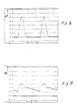
- the course of the current half-wave, current i1 via the rectifier D1 and the element L ', is shown in FIG. A timeline graduation corresponds to one microsecond (1E-6S / DIV) in FIGS. 2 to 11.
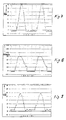
- the current i3 flowing through the smoothing capacitor CG is shown in FIG. It is a pure alternating current.
- the capacitor CR and the smoothing capacitor CG are routed together via the primary winding WI of an additional current transformer SW.
- this current transformer SI is designed as a toroidal core transformer
- the primary winding WI can be realized simply by plugging the common supply line of the capacitors CR and CG to the load terminal not directly connected to the smoothing inductor L through the remaining hole in the toroidal core.
- the current i3 generates a voltage drop UMESS on the secondary winding WII of the current transformer SW (FIG. 5), which is detected by the current measuring resistor RM.
- the AC voltage at the current measuring resistor RM is rectified in such a way that the voltage plateau proportional to the load current is peak-integrated (rectifier D2, resistor R1, capacitor C1 in FIG. 12).
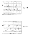
- the remaining oscillograms show the drain voltage UDrain at the field effect transistor S1 (FIG. 8), the voltage U3 at the output of the rectifier D1 (FIG. 9), the current i4 from Connection point of the inductors L, L 'to the resonance capacitor CR ( Figure 10) and the voltage U5 across the smoothing inductor L ( Figure 11).
- the invention can of course also be used for a direct voltage converter without electrical isolation, in which the transformer Tr is omitted.
- the controller for controlling the switching regulator actuator S1 consists of a VCO (voltage controlled oscillator), to which the peak current-integrated voltage proportional to the capacitor C1, possibly amplified via a control amplifier RV, can be supplied as a control voltage.
- a monoflop MF is connected downstream of the VCO and is triggered by the output signal of the VCO. With this arrangement, the switching regulator actuator S1 is supplied with switch-on pulses of constant duration.
- the switch-off duration of the switching regulator actuator S1 is variable and depends on the output voltage UA. A high output voltage UA leads to a long switch-off duration of the switching regulator actuator S1 and a low output voltage UA leads to a short switch-off duration.
- the energy supply to the controller can take place during the time during which a sufficiently high current i2 flows through the smoothing inductor L via an additional winding W1 on the core of the smoothing inductor L.
- the winding W1 is connected to a rectifier D3 and a storage capacitor C2.
- the drain-source path of the field effect transistor S1 is connected to the Series circuit consisting of the rectifier D4 and the capacitor C3 connected.
- the connection point of rectifier D4 and capacitor C3 is connected via resistor R2 to the positive potential terminal of the DC voltage source QE. This circuit enables the demagnetization energy of the transformer Tr to be fed back to the DC voltage source QE.
Landscapes
- Engineering & Computer Science (AREA)
- Power Engineering (AREA)
- Dc-Dc Converters (AREA)
Description
- Die Erfindung betrifft einen Gleichspannungswandler gemäß dem Oberbegriff des Patentanspruchs 1.
Solche Gleichspannungswandler sind bekannt (EP 0330 987; IEEE Power Electronics Specialists Conference, Université Paul Sabatier, Toulouse, France, 1985, Seiten 106 bis 116). - Gleichspannungswandler vom Zerhackerprinzip werden zur Erhöhung der Arbeitsfrequenz mit induktiven und kapazitiven Elementen beschaltet, um das Stellglied im Nulldurchgang verlustfrei schalten zu können. Durch die zusätzliche Beschaltung werden quasi-sinusförmige Ströme eingeprägt.
- Der Erfindung liegt die Aufgabe zugrunde einen derartigen Gleichspannungswandler so auszubilden, daß er ein gutes dynamisches Verhalten aufweist, d.h. sich auf schnelle Laständerungen einstellen kann. Diese Aufgabe wird durch die Merkmale des Patentanspruchs 1 gelöst. In den Unteransprüchen sind vorteilhafte Aus-/Weiterbildungen aufgezeigt.
- Der Gleichspannungswandler nach der Erfindung zeichnet sich dadurch aus, daß während der Energieübertragungsphase des Gleichspannungswandlers - Stellglied eingeschaltet - ein Teil des Resonanzstromes unverzögert, d.h. ohne Phasendrehung direkt in den ausgangsseitigen Glättungskondensator, beziehungsweise zur Last fließen kann. Dies bedeutet, daß der Einfluß der Phasendrehung der Glättungsdrossel erheblich verringert ist. Dies erhöht die Phasenreserve des Regelkreises und verbessert das dynamische Verhalten des Reglers, insbesondere bei Lastsprüngen.
Während der Energieübertragung des Gleichspannungswandlers - Stellglied geschlossen - arbeitet die Glättungsdrossel auch als Stromwandler. Die Induktivität des zusätzlichen induktiven Elements bzw. ein Teil der Glättungsdrossel bestimmt in Verbindung mit dem kapazitiven Element im wesentlichen die Resonanzfrequenz der Stromhalbwelle. Die Streuinduktivität des zusätzlichen Stromwandlers ist dabei vernachlässigbar. Nach Öffnen des Stellgliedes arbeitet nur noch die Glättungsdrossel. - Anhand der Zeichnungen wird die Erfindung nun näher erläutert.
- Es zeigen
- Figur 1
- ein Prinzipschaltbild des Gleichspannungswandlers nach der Erfindung,
- Figur 2 bis Figur 11
- ausgewählte Oszillogramme von Strom- und Spannungsverläufen beim Gleichspannungswandler nach der Erfindung,
- Figur 12
- ein Prinzipschaltbild des Gleichspannungswandlers nach der Erfindung mit günstiger Laststromauswertung.
- Der in Figur 1 dargestellte Quasi-Resonanzwandler arbeitet nach dem Flußwandlerprinzip mit galvanischer Trennung zwischen Gleichspannungsversorgungskreis und Gleichspannungs-Lastkreis. Die Gleichspannungsquelle QE ist über das Schaltregler-Stellglied S1 mit der Primärwicklung t1 des Transformators Tr verbunden. Die Sekundärwicklung t2 des Transformators Tr ist über die Serienschaltung aus Gleichrichter D1 und Glättunsdrossel L mit dem ausgangsseitigen Glättungskondensator CG, der parallel zur Last RL liegt, verbunden. Die beim Flußwandler übliche Freilaufdiode ist mit DF bezeichnet.
Parallel zur Freilaufdiode DF ist das resonanzbestimmende kapazitive Element - Kondensator CR - des Quasi-Resonanzwandlers angeordnet. Das induktive resonanzbestimmende Element des Quasi-Resonanzwandlers ist entweder Teil der Glättungsdrossel L oder ein mit der Glättungsdrossel L magnetisch gekoppeltes zusätzliches induktives Element L'. Wie in Figur 1 dargestellt, liegt das induktive Element L' zwischen dem Gleichrichter D1 und dem Verbindungspunkt der Kathode der Freilaufdiode DF mit der Glättungsdrossel L. Der Wicklungssinn der Wicklung auf dem Element L' ist bezüglich des Wicklungssinns der Wicklung auf der Glättungsdrossel L - in Figur 1 durch einen Punkt markiert - derart, daß während der Energieübertragung des Gleichspannungswandlers - das Schaltregler-Stellglied S1 ist dann geschlossen - ein Teil des Resonanzstromes zum Ausgang des Gleichspannungswandlers, beziehungsweise in dessen ausgangsseitigen Glättungskondensator CG fließen kann. Die Glättungsdrossel L arbeitet zusammen mit dem induktiven Element L' als Stromwandler. Die Induktivität des induktiven Elements L' bestimmt in Verbindung mit dem Kondensator CR im wesentlichen die Resonanzfrequenz der Stromhalbwelle. Das Verhältnis der Windungszahl der Wicklung auf der Glättungsdrossel L zur Windungszahl der Wicklung auf dem zusätzlichen induktiven Element L' wird größer als 1, z.B. 4 gewählt. Dieses Verhältnis wird entsprechend der Anwendung bezüglich des Wirkungsgrades und den dynamischen Eigenschaften optimiert. Der Verlauf der Stromhalbwelle, Strom i1 über den Gleichrichter D1 und das Element L', ist in Figur 2 dargestellt. Ein Zeitachsenteilstrich entspricht in den Figuren 2 bis 11 einer Mikrosekunde (1E-6S/DIV). Der Verlauf des Laststroms i2, der über die Glättungsdrossel L fließt, ist in Figur 3 dargestellt. Für eine realisierte Schaltung betrug der Mittelwert dieses Laststroms
- In einer Ausgestaltung der Erfindung (Fig. 12) ist der Kondensator CR und der Glättungskondensator CG gemeinsam über die Primärwicklung WI eines zusätzlichen Stromwandlers SW geführt. Ist dieser Stromwandler SI als Ringkernübertrager ausgebildet, so kann die Primärwicklung WI einfach dadurch realisiert werden, daß die gemeinsame Zuleitung der Kondensatoren CR und CG zu der nicht unmittelbar mit der Glättungsdrossel L verbundenen Lastklemme durch das Restloch des Ringkerns gesteckt wird. Der Strom i3 erzeugt an der Sekundärwicklung WII des Stromwandlers SW einen Spannungsabfall UMESS (Figur 5), der mit dem Strommeßwiderstand RM erfasst wird. Die Wechselspannung am Strommeßwiderstand RM wird so gleichgerichtet, daß das dem Laststrom proportionale Spannungsplateau spitzenwertintegriert wird (Gleichrichter D2, Widerstand R1, Kondensator C1 in Figur 12).
- Wenn das Schaltregler-Stellglied S1, das hier als Feldeffekttansistor ausgebildet ist, geöffnet wird (

- Die übrigen Oszillogramme zeigen die Drainspannung UDrain am Feldeffekttransistor S1 (Figur 8), die Spannung U3 am Ausgang des Gleichrichters D1 (Figur 9), den Strom i4 vom Verbindungspunkt der Induktivitäten L, L' zum Resonanzkondensator CR (Figur 10) und die Spannung U5 über der Glättungsdrossel L (Figur 11).
- Die Erfindung ist natürlich auch für einen Gleichspannungswandler ohne galvanische Trennung, bei dem der Transformator Tr entfällt, anwendbar.
Der Regler zur Steuerung des Schaltregler-Stellgliedes S1 besteht aus einem VCO (voltage controlled oscillator), dem die spitzenwertintegrierte laststromproportionale Spannung am Kondensator C1, gegebenenfalls verstärkt über einen Regelverstärker RV, als Steuerspannung zugeführt werden kann. Dem VCO ist ein Monoflop MF nachgeschaltet, das von dem Ausgangssignal des VCO getriggert wird. Mit dieser Anordnung wird das Schaltregler-Stellglied S1 mit Einschaltimpulsen konstanter Dauer versorgt. Die Ausschaltdauer des Schaltregler-Stellgliedes S1 ist variabel und von der Ausgangsspannung UA abhängig. Eine hohe Ausgangsspannung UA führt zu einer langen Ausschaltdauer des Schaltregler-Stellgliedes S1 und eine niedrige Ausgangsspannung UA zu einer kurzen Ausschaltdauer. - Die Energieversorgung des Reglers kann für die Zeit während der ein ausreichend hoher Strom i2 durch die Glättungsdrossel L fließt über eine zusätzliche Wicklung W1 auf dem Kern der Glättungsdrossel L erfolgen. Hierzu ist die Wicklung W1 mit einem Gleichrichter D3 und einem Speicherkondensator C2 beschaltet. Beim Anlaufen oder bei Kurzschluß am Ausgang wird die Energieversorgung des Reglers aus der Gleichspannungsquelle QE über einen Hilfsregler HR aufrecht erhalten.
- Zur Abmagnetisierung des Transformators Tr ist die Drain-Source Strecke des Feldeffekttransistors S1 mit der Serienschaltung bestehend aus dem Gleichrichter D4 und dem Kondensator C3 beschaltet. Der Verbindungspunkt von Gleichrichter D4 und Kondensator C3 ist über den Widerstand R2 mit der Pluspotential führenden Klemme der Gleichspannungsquelle QE verbunden. Durch diese Beschaltung ist es möglich die Abmagnetisierungsenergie des Transformators Tr auf die Gleichspannungsquelle QE zurückzuspeisen.
Claims (5)
- Gleichspannungswandler vom Typ eines Quasi-Resonanzwandlers, mit einem induktiven und einem kapazitiven resonanzbestimmenden Element mit einer Glättungsdrossel, einer Freilaufdiode und einem Glättungskondensator, dadurch gekennzeichnet, daß das induktive resonanzbestimmende Element (L') Teil der Glättungsdrossel (L) im Lastkreis des Gleichspannungswandlers oder ein mit der Glättungsdrossel (L) magnetisch gekoppeltes zusätzliches induktives Element ist, wobei der Wicklungssinn der Wicklung auf dem induktiven resonanzbestimmenden Element (L') bezüglich des Wicklungssinnes der Wicklung auf der Glättungsdrossel (L) derart gewählt ist, daß während der Energieübertragung des Gleichspannungswandlers ein Teil des Resonanzstromes zum Ausgang des Gleichspannungswandlers, beziehungsweise in dessen ausgangsseitigen Glättungskondensator (CG), fließen kann, daß das kapazitive resonanzbestimmende Element (CR) und die Freilaufdiode (DF) des Gleichspannungswandlers vom ausgangsseitigen Glättungskondensator (CG) über die Glättungsdrossel (L) und von der Eingangsseite durch das induktive resonanzbestimmende Element (L') entkoppelt sind.
- Gleichspannungswandler nach Anspruch 1, dadurch gekennzeichnet, daß das Verhältnis der Windungszahl der Wicklung auf der Glättungsdrossel (L) zur Windungszahl der Wicklung auf dem zusätzlichen induktiven resonanzbestimmenden Element (L') größer als eins, z.B. vier, gewählt ist.
- Gleichspannungswandler nach Anspruch 1 oder 2, dadurch gekennzeichnet, daß der Gleichspannungswandler einen Regelkreis aufweist zur Steuerung des Gleichspannungswandler-Stellgliedes (S1) in Abhängigkeit der Ausgangsspannung (UA) des Gleichspannungswandlers in dem Sinne, daß das Stellglied (S1) mit konstanter Einschaltzeit und variabler Ausschaltzeit betreibbar ist, wobei bei hoher Ausgangsspannung (UA) eine lange Ausschaltzeit und bei niedriger Ausgangsspannung (UA) eine kurze Ausschaltzeit vorgebbar ist.
- Gleichspannungswandler nach einem der Ansprüche 1 bis 3, dadurch gekennzeichnet, daß die Glättungsdrossel (L) eine zusätzliche Wicklung (W1) aufweist über welche die Energieversorgung des Reglers zumindest teilweise erfolgen kann.
- Gleichspannungswandler nach einem der Ansprüche 1 bis 4, dadurch gekennzeichnet, daß das resonanzbestimmende kapazitive Element (CR) und der ausgangsseitige Glättungskondensator (CG) des Gleichspannungswandlers an ihrem Fußpunkt miteinander verbunden und gemeinsam über die Primärwicklung (WI) eines zusätzlichen Stromwandlers (SW) geführt sind, welcher zur Gewinnung eines laststromproportionalen Signals vorgesehen ist.
Applications Claiming Priority (2)
| Application Number | Priority Date | Filing Date | Title |
|---|---|---|---|
| DE3941420A DE3941420C1 (de) | 1989-12-15 | 1989-12-15 | |
| DE3941420 | 1989-12-15 |
Publications (3)
| Publication Number | Publication Date |
|---|---|
| EP0432603A2 EP0432603A2 (de) | 1991-06-19 |
| EP0432603A3 EP0432603A3 (en) | 1991-09-25 |
| EP0432603B1 true EP0432603B1 (de) | 1994-08-03 |
Family
ID=6395518
Family Applications (1)
| Application Number | Title | Priority Date | Filing Date |
|---|---|---|---|
| EP90123065A Expired - Lifetime EP0432603B1 (de) | 1989-12-15 | 1990-12-01 | Gleichspannungswandler, insbesondere vom Typ eines Quasi-Resonanzwandlers |
Country Status (2)
| Country | Link |
|---|---|
| EP (1) | EP0432603B1 (de) |
| DE (1) | DE3941420C1 (de) |
Cited By (1)
| Publication number | Priority date | Publication date | Assignee | Title |
|---|---|---|---|---|
| WO2008047186A2 (en) * | 2006-06-16 | 2008-04-24 | Astec Custom Power (Hk) Ltd. | A zero voltage zero current switching converter |
Families Citing this family (3)
| Publication number | Priority date | Publication date | Assignee | Title |
|---|---|---|---|---|
| FR2710435B1 (fr) * | 1993-09-24 | 1995-12-22 | Neopost Ind | Machine à affranchir comportant un circuit de verrouillage de sécurité. |
| JP2868422B2 (ja) * | 1993-10-28 | 1999-03-10 | ヴィエルティー コーポレーション | 電力変換における電流検出装置及び方法 |
| US9948192B2 (en) | 2016-05-04 | 2018-04-17 | Toyota Motor Engineering & Manufacturing North America, Inc. | Quasi-resonant operation of a power conversion circuit including switches symmetrically arranged about a transformer |
Family Cites Families (3)
| Publication number | Priority date | Publication date | Assignee | Title |
|---|---|---|---|---|
| US1920948A (en) * | 1928-01-27 | 1933-08-01 | Byrnes Townsend & Potter | Electrical filter |
| US3652958A (en) * | 1969-04-23 | 1972-03-28 | Gen Systems Inc | Load filter network |
| US4951186A (en) * | 1988-03-04 | 1990-08-21 | Siemens Aktiengesellschaft | Single-ended forward frequency converter with a transformer and a demagnetization means |
-
1989
- 1989-12-15 DE DE3941420A patent/DE3941420C1/de not_active Expired - Lifetime
-
1990
- 1990-12-01 EP EP90123065A patent/EP0432603B1/de not_active Expired - Lifetime
Cited By (2)
| Publication number | Priority date | Publication date | Assignee | Title |
|---|---|---|---|---|
| WO2008047186A2 (en) * | 2006-06-16 | 2008-04-24 | Astec Custom Power (Hk) Ltd. | A zero voltage zero current switching converter |
| WO2008047186A3 (en) * | 2006-06-16 | 2008-07-10 | Astec Custom Power Hk Ltd | A zero voltage zero current switching converter |
Also Published As
| Publication number | Publication date |
|---|---|
| EP0432603A2 (de) | 1991-06-19 |
| EP0432603A3 (en) | 1991-09-25 |
| DE3941420C1 (de) | 1991-04-11 |
Similar Documents
| Publication | Publication Date | Title |
|---|---|---|
| DE102013111348B4 (de) | Verfahren und Schaltungsanordnung zum Ermitteln einer Entmagnetisierungsnullstromzeit | |
| DE19545154C2 (de) | Stromversorgungseinrichtung | |
| EP1257048B1 (de) | Regelvorrichtung für einen resonanten Konverter | |
| DE60101077T2 (de) | Schaltnetzteil mit Reihenkondensator | |
| DE3642634A1 (de) | Eintakt-gleichstromumrichter mit verlustloser umschaltung | |
| DE19882461B3 (de) | Verfahren und Schaltung zum Betrieb eines Transistors als Gleichrichter | |
| EP0422274A1 (de) | Verfahren zum Steuern von Gegentakt-Serien-Resonanzwandler-Schaltnetzteilen mit geregelter Ausgangsspannung | |
| DE60101234T2 (de) | Schaltnetzteilgerät | |
| EP0355333A2 (de) | Verfahren zum Betreiben eines Schaltreglers | |
| DE102017103264A1 (de) | Leistungswandler mit Nullspannungsschaltsteuerung | |
| EP0967714A2 (de) | Schaltnetzteil | |
| DE2756289A1 (de) | Stromversorgungsschaltung mit einem dc/ac-umsetzer | |
| DE10328782B4 (de) | Steuerschaltung für einen MOSFET zur Synchrongleichrichtung | |
| EP0374400B1 (de) | Anordnung zum Regeln des Stromes durch einen Verbraucher sowie Anwendung | |
| DE102006038474A1 (de) | Stromrichter | |
| EP0437884A2 (de) | Gleichspannungssperrwandler | |
| EP1701434A2 (de) | Ansteuerschaltung für den Schalter in einem Schatznetzteil | |
| DE19824409A1 (de) | AC-DC-Wandler | |
| DE10065421B4 (de) | Tiefsetzsteller | |
| DE19925490A1 (de) | Konverter mit Resonanzkreiselelementen | |
| EP0201878A2 (de) | Schaltungsanordnung mit einem p-schaltenden n-Kanal MOS-Transistor | |
| EP0432603B1 (de) | Gleichspannungswandler, insbesondere vom Typ eines Quasi-Resonanzwandlers | |
| DE102020120530A1 (de) | Hochsetzsteller-Schaltungsanordnung, Stromversorgung und Verfahren zur Auswärtswandlung einer Eingangsspannung | |
| DE10221450A1 (de) | Schaltungsanordnung für einen resonanten Konverter und Verfahren zu dessen Betrieb | |
| EP0432602B1 (de) | Gleichspannungswandler, insbesonder vom Typ eines Quasi-Resonanzwandlers |
Legal Events
| Date | Code | Title | Description |
|---|---|---|---|
| PUAI | Public reference made under article 153(3) epc to a published international application that has entered the european phase |
Free format text: ORIGINAL CODE: 0009012 |
|
| 17P | Request for examination filed |
Effective date: 19901228 |
|
| AK | Designated contracting states |
Kind code of ref document: A2 Designated state(s): FR GB IT NL |
|
| PUAL | Search report despatched |
Free format text: ORIGINAL CODE: 0009013 |
|
| AK | Designated contracting states |
Kind code of ref document: A3 Designated state(s): FR GB IT NL |
|
| 17Q | First examination report despatched |
Effective date: 19930623 |
|
| GRAA | (expected) grant |
Free format text: ORIGINAL CODE: 0009210 |
|
| ITF | It: translation for a ep patent filed |
Owner name: BARZANO' E ZANARDO MILANO S.P.A. |
|
| AK | Designated contracting states |
Kind code of ref document: B1 Designated state(s): FR GB IT NL |
|
| ET | Fr: translation filed | ||
| GBT | Gb: translation of ep patent filed (gb section 77(6)(a)/1977) |
Effective date: 19941028 |
|
| PLBE | No opposition filed within time limit |
Free format text: ORIGINAL CODE: 0009261 |
|
| STAA | Information on the status of an ep patent application or granted ep patent |
Free format text: STATUS: NO OPPOSITION FILED WITHIN TIME LIMIT |
|
| 26N | No opposition filed | ||
| PGFP | Annual fee paid to national office [announced via postgrant information from national office to epo] |
Ref country code: NL Payment date: 19961223 Year of fee payment: 7 |
|
| PG25 | Lapsed in a contracting state [announced via postgrant information from national office to epo] |
Ref country code: NL Free format text: LAPSE BECAUSE OF NON-PAYMENT OF DUE FEES Effective date: 19980701 |
|
| NLV4 | Nl: lapsed or anulled due to non-payment of the annual fee |
Effective date: 19980701 |
|
| PGFP | Annual fee paid to national office [announced via postgrant information from national office to epo] |
Ref country code: GB Payment date: 20001123 Year of fee payment: 11 |
|
| PGFP | Annual fee paid to national office [announced via postgrant information from national office to epo] |
Ref country code: FR Payment date: 20001212 Year of fee payment: 11 |
|
| PG25 | Lapsed in a contracting state [announced via postgrant information from national office to epo] |
Ref country code: GB Free format text: LAPSE BECAUSE OF NON-PAYMENT OF DUE FEES Effective date: 20011201 |
|
| REG | Reference to a national code |
Ref country code: GB Ref legal event code: IF02 |
|
| GBPC | Gb: european patent ceased through non-payment of renewal fee |
Effective date: 20011201 |
|
| PG25 | Lapsed in a contracting state [announced via postgrant information from national office to epo] |
Ref country code: FR Free format text: LAPSE BECAUSE OF NON-PAYMENT OF DUE FEES Effective date: 20020830 |
|
| REG | Reference to a national code |
Ref country code: FR Ref legal event code: ST |
|
| PG25 | Lapsed in a contracting state [announced via postgrant information from national office to epo] |
Ref country code: IT Free format text: LAPSE BECAUSE OF NON-PAYMENT OF DUE FEES Effective date: 20051201 |