EP0431416A2 - Gerät und Verfahren zur Realisierung eines zyklischen redundanten Parallel-Fehlerprüfungskodes - Google Patents
Gerät und Verfahren zur Realisierung eines zyklischen redundanten Parallel-Fehlerprüfungskodes Download PDFInfo
- Publication number
- EP0431416A2 EP0431416A2 EP90122381A EP90122381A EP0431416A2 EP 0431416 A2 EP0431416 A2 EP 0431416A2 EP 90122381 A EP90122381 A EP 90122381A EP 90122381 A EP90122381 A EP 90122381A EP 0431416 A2 EP0431416 A2 EP 0431416A2
- Authority
- EP
- European Patent Office
- Prior art keywords
- control signal
- error check
- check code
- signal
- storage
- Prior art date
- Legal status (The legal status is an assumption and is not a legal conclusion. Google has not performed a legal analysis and makes no representation as to the accuracy of the status listed.)
- Withdrawn
Links
Images


Classifications
-
- H—ELECTRICITY
- H03—ELECTRONIC CIRCUITRY
- H03M—CODING; DECODING; CODE CONVERSION IN GENERAL
- H03M13/00—Coding, decoding or code conversion, for error detection or error correction; Coding theory basic assumptions; Coding bounds; Error probability evaluation methods; Channel models; Simulation or testing of codes
- H03M13/03—Error detection or forward error correction by redundancy in data representation, i.e. code words containing more digits than the source words
- H03M13/05—Error detection or forward error correction by redundancy in data representation, i.e. code words containing more digits than the source words using block codes, i.e. a predetermined number of check bits joined to a predetermined number of information bits
- H03M13/09—Error detection only, e.g. using cyclic redundancy check [CRC] codes or single parity bit
- H03M13/091—Parallel or block-wise CRC computation
Definitions
- the present invention broadly relates to a cyclic redundancy error check code generator and more particularly, the invention relates to a cyclic error check code generator which processes byte-wide data in parallel and provides means for accessing the cyclic error check code generated.
- Errors may be introduced during the reading, writing, or actual transmission process. Error control has become an integral part of the design of computers and communication systems.
- One method employed for error detection involves the addition of one or more bits, called redundancy bits, at the end of the block of information-carrying bits. The redundancy bits do not carry any data information; they are merely used to determine the correctness of the bit stream carrying the information.
- Cyclic redundancy checking is an algorithmic error-detecting technique used to verify that the digital information received is correct.
- a digital data word ( d ) is written as a polynomial D(x) where each of the data bits are the coefficients for each term.
- the data polynomial D(x) is divided modulo 2 by a predetermined generator polynomial G(x) and a remainder R(x) of this division is appended to the digital data word d as a cyclic redundancy check (CRC) character.
- the remainder which is shorter than the original polynomial, is a unique number for each data word.
- the CRC included in a message is compared with the CRC character obtained at the receiving end by performing the same division. If the two CRCs agree, the message is assumed correct. If they disagree, the receiving terminal will take some appropriate action.
- the (L - 1)-degree polynomial D(x) is:
- the CRC may be a single character or r bits, where r ⁇ L.
- D(x) is multiplied by x r as this is equivalent to shifting the message bits r places to the left.
- G(x) be the "generator” or "checking" polynomial of degree r, whose coefficients are also 0 or 1.
- the shifted polynomial data D(x) is divided by G(x) obtaining: where:
- W(x) is of degree r + L - 1, and contains the original L message bits (the x r D(x) term) and r check bits (the R(x) term). Furthermore, W(x) is exactly divisible by G(x). The coefficients of W(x) is what is transmitted. On the receiving end, W(x) is also divided by G(x), and the remainder in this case must be 0; otherwise, if a remainder is generated, an error has occurred.
- Some systems notably FDDI, actually transmit the 1's complement of the remainder rather than the remainder itself.
- the receiver compares the calculated remainder of the transmitted word against an expected constant value and report an error if there is a mismatch.
- Such systems are more robust against spurious strings of zeros being added to the end of any message.
- Parallel bit CRC processing wherein a plurality of data bits are read in parallel and shifted in parallel, to generate an error checking code is well known.
- n bits in parallel By shifting n bits in parallel, one shift in the parallel circuitry is equivalent to n shifts in a serial system.
- certain of the hardware elements may be shared.
- the CRC generating circuitry may employ a plurality of shift registers, used in conjunction with exclusive OR-type logic elements to generate the CRC since the data received is binary data.
- the input data bits are respectively received in parallel and the error code generating circuit is arranged according to the particular generator polynomial employed to generate the error check code. Patel teaches that for any polynomial G(x) with a degree of r, a parallel feedback shift register circuit can be generated which processes Y bits in parallel (where Y is ⁇ ⁇ r).
- Patel does not teach or suggest how to read out the error check code generated for the last data byte received.
- an error checking encoding and decoding circuit may receive a plurality of input bits in parallel and generate a CRC by processing the data in parallel.
- the bits are read into a first set exclusive-OR gates and its output is input into a second set of exclusive-OR gates.
- the output from the second set of exclusive-OR gates are input into a third set of exclusive-OR gates, where each set has eight exclusive-OR gates since 8 bits of data are processed in parallel.
- the signals out of the third set of gates are transferred into flip-flops and on the second clock pulse, the signals are shifted from the first set of flip-flops to a second set of flips.
- the output from the two sets of flip-flops are coupled to AND gates where the signals are ANDed to produce the CRC signal. While the system generates a CRC by processing multiple bits in parallel, the system does not share hardware elements.
- An approach which may be employed to read out the stored error code signal is to "create a 4 deep by 8-bit wide shift register out of the storage elements by installing 2-input MUXes on the inputs of the top 24 storage devices.
- One of the two inputs to each MUX would come from the logic that had previously been wired into the input of the storage element.
- the other input would come directly from the output of the storage element 8 positions earlier.
- the disadvantages of this approach is that it requires 24 MUXes which take up room in an implementation, consume power, and add delay to the logic path, potentially limiting execution speed.”
- a plurality of data information bits are input to a shift register and modulo 2 added to an input distribution matrix, B.
- the input distribution matrix B determines how an input data bit stream I will be added to a state transition matrix A where the current state information is stored to generate the next state information S m+z .
- the input distribution matrix B is comprised of a plurality of logic elements and shift registers which are configured based upon the generator polynomial G(x) employed to generate a cyclic redundancy error check code which is appended to the information data bit stream to be transmitted.
- the state transition matrix is also comprised of a plurality of logic elements and shift registers. In implementing the A and B matrices in hardware, the system makes use of the fact that the input distribution matrix B is related to the state transition matrix A in that the columns of the B matrix make up a proper subset of the columns of the A matrix.
- the data is shifted through the storage registers and a portion of the error check code is presented to a Z-bit wide x 2 input multiplexor.
- To further shift the remainder of the error check code without further modification requires that logical zero signals be applied to logical exclusive OR gates at the input to certain of the storage registers.
- the zeros may be forced by applying a logical zero signal to one input of each of a plurality AND gates at the output of the input distribution matrix or, by applying a logical zero signal to one input of each of a plurality AND gates at the input to the input distribution matrix.
- the number of AND gates required at the input to the B matrix is less than the number of AND gates at the output of the B matrix.
- a primary object of the present invention is to provide a cyclic redundancy error code generating system which processes parallel data, shares common logic circuitry, and which provides means for reading out of storage during subsequent clock cycles, the generated error code without modifying it.
- the error check code is appended to the data word being transmitted.
- the error check code (i.e., the final state of the error code generator system) is S L .
- S L S m .
- the state bits S are set to some predetermined value, S 0 . That value is often zero; however, in the preferred embodiment (and in FDDI) it is all ones.
- Each bit of the data stream causes a change in state according to Equation 10.
- the state value S L is equal to the remainder polynomial (or error check code).
- Equations 11 and 12 a j,k is the element in the j th row of the k th column of matrix A and a j is the coefficient of the j th term in the generator polynomial G(x).
- the state transition matrix A is an n x n matrix of coefficients (or elements), where n is the largest power in the generator polynomial G(x).
- each term z j,k in the resulting matrix Z is formed by calculating the cross product of the j th row of the first matrix operand and the k th column of the second matrix operand.
- the cross product is calculated by logically ANDing together the pairs of corresponding elements and then logically EXCLUSIVE-ORing those results together. If one of the operands is a scalar rather than a matrix, then the product is formed by multiplying each element of the operand matrix by the scalar.
- the elements of the resulting matrix or vector is formed by logically EXCLUSIVE-ORing together the corresponding elements of the two matrices or vectors.
- an error check code generating system utilizes a generator polynomial employed G(x), a received data sequence I 0(L) , a distribution matrix B, a state transition matrix A, and current state information S , to generate an error check code S L corresponding to the entire bit stream I 0(L) ).
- next state S m+1 is calculated and replaces the prior S m value and becomes the current state information.
- generating the next state information for a sequence of data is an iterative process.
- the cyclic redundancy error check code generator of the present invention may be used in conjunction with a data transmission network, such as the Fiber Distributed Data Interface (FDDI), to determine the integrity of a received data transmission.
- FDDI Fiber Distributed Data Interface
- the Fiber Distributed Data Interface (FDDI) protocol is an American National Standards (ANS) data transmission standard which applies to a 100 megabit/second token ring network that utilizes an optical fiber transmission medium.
- the FDDI protocol is described in "FDDI-an Overview,” Digests of Papers IEEE Computer Society Int'l Conf. , Compcon '87 , Jan, 1987, which is herein incorporated by reference.
- the FDDI protocol is intended as a high performance interconnection among computers as well as among computers and their associated mass storage sub-systems and other peripheral equipment.
- Information is transmitted on an FDDI ring in "frames" that consist of a sequence of 5-bit data characters or "symbols.”
- Information is typically transmitted in symbol pairs or "bytes.” Tokens are used to signify the right to transmit data between stations.
- FDDI FDDI Media Access Control
- the state transition matrix A is directly related to the generator polynomial G(x) and the input distribution vector B is identical to column n - 1 of the A matrix.
- the preferred generator polynomial in Equation 14 A is a 32 x 32 matrix and B is a 32 x 1 vector.
- I m(z) (i m+z-1 , i m+z-2 , ... i
- S m+8 A8 x S m + B8 x I m(8) (20)
- S m+8 is the state of the generator after 8 input bits are processed in parallel
- A8 is the A matrix raised to the 8 th power
- B8 is the 32 x 8 matrix made up of the vectors B
- I m(8) is the 8 x 1 vector made up of the eight input bits starting with i m .
- the B8 matrix is identical to 8 columns of the A8 matrix because the operations that take place on A to form the A8 matrix are the same as the operations that take place on B to form the B8 matrix.
- the physical realization of the error check code generator of Equation 20 in hardware operates on eight input bits at a time.
- the input bits I m may be exclusive OR-ed with the 8 most significant bits of S m before the B8 matrix is applied.
- the hardware with which the 8 columns in the A8 matrix are implemented may be eliminated to avoid duplication of hardware elements.
- Equation 21 The realization of Equation 21 in hardware requires the following:
- the B z matrix 201 is identical to the Z highest columns in the state transition matrix 101.
- B z is identical to columns n-1 through n-z of the A matrix 101.
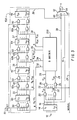
- an error check code generating system 300 for implementing Equation 21 in hardware, where 8 bits are processed in parallel (z 8), and common hardware elements are shared, is illustrated. It is recognized that those skilled in the art may arrive at various other systems for generating an error check code in accordance with Equation 20, or for generating an error check code where the error check code corresponds to the remainder terms which are stored in a storage element after the data sequence has been processed.
- the system 300 includes an input storage register 14, an input distribution matrix element 200 and a state transition matrix element 100.
- the logic elements used to implement the A matrix 101 which are the same as those used to implement the B matrix 201 may be shared.
- the state transition matrix element 100 and the input distribution matrix element 200 are both comprised of logic elements which implement the matrices in hardware.
- a plurality of state storage registers 40, 42, 44, 46 in the state transition matrix element 100 are preset by a PRESET control 51 to all ones by inserting a plurality of sets of logical OR gates 50 at the input of the state storage registers 40, 42, 44, 46.
- the state storage registers 40, 42, 44, 46 store a plurality of logic 1 signals and generate a plurality of current state signals 33, 35, 37, 39 which are also all logic 1's.
- a parallel input data signal (I z ) 12 comprised of z bits, defined as a data byte, is received by an input register 14 which has z input ports.
- a plurality of data bytes received over a plurality of clock cycles may comprise the data sequence I 0(L) for which the error check code S L is being generated.
- I 0(L) is comprised of bits i0 ... i L-1 .
- the input data byte signal 12 is 8 bits wide I0-I7 and therefore the input register 14 is an 8 bit storage register. Only one clock is needed because all of the input bits i m+7 - i m of the data byte 12 are read in parallel.
- a control signal 24 which controls a multiplexor (MUX) 52 issues a logic high signal or a "1" when the system 300 is receiving an input data byte 12 (i m+7 , ... i m) .
- the control signal 24 may either be a logic high or a logic low signal.
- the MUX 52 is an z-bit wide multiplexor. In the preferred embodiment, since eight bits are processed in parallel the MUX 52 is an 8-bit wide MUX. Similarily, since the MUX 52 selects between 2 input (signal 16 or signal 39) the MUX is an 8-bit 2 input wide MUX 52.
- the input register 14 is rising edge sensitive and upon receiving a rising edge clock signal (not illustrated), the input register 14 stores the data byte signal 12 received (i m+7 ... i m ) and it also outputs a data byte signal 16 having the same value as the data signal 12 received.
- the data byte signal 16 is modulo 2 added in parallel, via a plurality of exclusive-OR gates (XOR) 20, to a last one of a plurality of a current state remainder signals 39 (S24.31), where signals 39 are the top eight bits of S m (S 31,m - S 24,m ).
- the last current state signal 39 corresponds to bits N-1 through N-Z of the current state signal S m .
- the XOR gates 20 sum each bit in the signals 16, 39 together and a first summed Z-bit parallel signal 22 is generated.
- the first summed signal 22 is T 31,m -T 24,m .
- Both signals 39, 16 are added together to save logic elements because, according to Equation 14, both signals 16, 39 are multiplied by the input distribution matrix 200.
- the signals 16, 39 may be added together first before being multiplied.
- the first summed signal 22 is modulo 2 multiplied with the control signal 24 to generate a Z-bit controlled sum signal 28 where, in the preferred embodiment the controlled sum signal 28 is T' 31,m - T' 24,m .
- the modulo 2 multiplication is accomplished by a plurality of logical AND gates 26 which each logically AND together the control signal 24 and each bit of the first summed signal 22.
- control signal 24 is a logic 1
- the Z-bit controlled sum signal 28 is identical to the Z-bit parallel first summed signal 22. If the control signal 24 is a 0, then the controlled sum signal 28 is a 0.
- the Z-bit parallel controlled sum signal 28 is input to the input distribution matrix element 200 where it is multiplied by the input distribution matrix (B8 matrix) 201.
- the remainder terms generated by the B matrix multiplication comprise an N-bit parallel distribution signal B0 - B31.
- the B matrix 201 calculates the 8 highest columns of the A8 matrix and presents those 32 output signals (distribution signals 32, 34, 36, 38) as the 4-sets of 8 bit distribution signals.
- the distribution signals 32, 34, 36, 38 are a partial sum in that they represent the cross product of the highest 8 bits of the T matrix with the highest 8 columns of the A8 matrix (i.e., columns 31-24).
- the input distribution matrix 201 converts the Z-bit parallel controlled sum signal 28 into an N-bit parallel distribution signal B0 - B31.
- a first one of the parallel distribution signals corresponds to bits 0-7 (B0.7) of the distribution signal and is herein referred to as "the first distribution signal 32";
- a second one of the signals corresponds to bits 8-15 (B8.15) and is herein referred to as “distribution signal 34";
- a third one of the parallel signals corresponds to bits 16-23 (B16.23) and is herein referred to as “distribution signal 36";
- a fourth one of the parallel signals corresponds to bits 24-31 (B24.31) and is herein referred to as "the last distribution signal 38".
- S m enters the state storage registers 40, 42, 44, 46 and i m enters the input storage register 14.
- the values of S m+8 are calculated and presented to the input of storage registers 40, 42, 44, 46 so that on the next clock stroke, S m+8 is clocked into registers 40, 42, 44, 46.
- all of the distribution signals 34, 36, 38 generated in that clock cycle, except for the first distribution signal 32, are modulo 2 added by logical exclusive OR gates (XOR) 60a, 60b, 60c respecitively with a plurality of current state remainder signals S m 33, 35, 37 (generated in the previous clock cycle but stored in the registers at the end of that clock cycle) read out of the plurality of state transition storage registers 40, 42, 44.
- XOR logical exclusive OR gates
- the first distribution signal 32 which represents the 0 - 7 rows of the 8 highest columns of the A8 matrix, is presented directly to storage register 40 (since the preset signal is 1).
- the highest 8 columns are identical to the B8 matrix.
- the second distribution signal 34 which is the 8 - 15 rows of the highest 8 columns of the A8 matrix is XORed, via a plurality of XOR gates 60a, with the current state remainder signal s 0,m - s 7,m 33 output by register 40.
- the remainder terms 41 generated by this matrix multiplication is s 8,m+8 ...s 15,m+8 .
- the remainder terms 41 are available at the input of register 42 but will not be stored into the register 42 until the next clock cycle. (On the next clock cycle s 8,m+8 ...s 15,m+8 are stored into register 42.
- the third distribution signal 36 is the 16-23 rows of the highest 8 columns of the A8 matrix.
- the third distribution signal is XORed, via a plurality of XOR gates 60b, with the current state remainder signal 35 s 8,m - s 15,m output by register 42.
- the remainder terms 43 generated by this matrix multiplication are s 16,m+8 ...s 23,m+8 . They are available at the input of register 44 but, again, are not stored into the register 44 until the next clock cycle. (On the next clock cycle s 16,m+8 ...s 23,m+8 are stored into register 44.
- the last distribution signal 38 represents the value of the highest 8 rows (rows 24-31) of the highest 8 columns of the A8 matrix.
- the last distribution signal 38 is XORed, via a plurality of XOR gates 60c, with the current state remainder signal 37 output by register 44.
- the current state remainder signal 37 is s 16,m - s 23,m .
- the remainder terms 45 generated by this matrix multiplication are s 24,m+8 ...s 31,m+8 and they are available at the input of last state register 46 but, on the next clock cycle s 24,m+8 ... s31,m+8 are stored into register 46.
- the storage elements 40, 42, 44, 46 of the generator 300 contain the remainder terms or error check code S L for the data sequence I 0(L) .
- the first approach places a two-input MUX at the input of each of the top 24 outputs of storage elements 42,44, 46.
- the MUX is controlled with the same signal that controls the 8 output MUXes.
- These 24 MUXes would choose either the EXCLUSIVE-OR gates 60a, 60b, 60c that normally feed the input to the storage elements or the output of the corresponding storage element in the next lower rank. This approach allows the data to shift through the storage elements on the subsequent clock strokes.
- the second approach makes use of the fact that the 24 EXCLUSIVE-OR gates already tie the top 24 outputs of storage elements 42, 44, 46 to the corresponding elements in the next lower rank.
- the third approach which is the approach employed in the preferred embodiment (shown in Figure 3), makes use of the fact that forcing the highest 8 bits of the T vector to zero also forces the outputs of the B-Matrix to zero, thereby having the same effect as the 24 2-input AND gates in the second approach.
- the third approach is more efficient since it only requires 8 2-input AND gates.
- the contents of the state storage registers 40, 42, 44, 46 are read out in parallel as the N-bit current state signals 33, 35, 37, 39 forming S m .
- Each of the state storage registers 40, 42, 44, 46 outputs Z-bits of the N-bit current state signal S m .
- the remainder terms generated by the matrix multiplication 41, 43, 45 are stored in a plurality of the state storage registers 42, 44, 46 and the first distribution signal 32 stored in register 40 are the N-bit next state signal s m+8 .
- the first distribution signal 32 is stored in parallel in the first one of the Z-bit state storage register 40 without being logically XOR-ed with Z-bits of the current state remainder signal, S m .
- the N-bit parallel distribution signal 32, 34, 36, 38 is modulo 2 multiplied with N-Z rows of the state transition matrix 101.
- XOR the first distribution signal 32 since, as previously discussed, it corresponds to the bottom z rows of the state transition matrix (rows 0-7) 201.
- the state transition matrix element 100 is a 32 x 32 matrix which is realized in hardware using a plurality of logical XOR gates 50. There is one logical XOR gate 50 for each bit of the parallel 8-bit distribution signals 34, 36, 38 (excluding the first distribution signal 32) that are received by the state transition matrix element 100.
- the state transition matrix element 100 also includes a 4-8 bit state storage register 42, 44, 46, 48 for simultaneously storing the 24 remainder terms generated by the matrix multiplication and the first distribution signal 32.
- Each of the state storage registers 40, 42, 44, 46, 48 outputs 8-bits of the 32 bit state signal 33, 35, 37, 39, respectively.
- the input distribution matrix element 200 is a 32 x 8 matrix which is also implemented in hardware using conventional techniques, such as a plurality of logical exclusive OR elements (not illustrated).
- the distribution matrix element 200 is configured similar to the state transition matrix element 100, however, in the preferred embodiment, it does not include storage registers.
- the off diagonal of 1's section of the state transition matrix 101 is implemented in hardware by XOR-gates, where the 1st bit position is XORed with the 9th bit position, the 2nd bit position is XORed with the 10th bit position, the 3rd bit is XORed with the 11th bit position, etc. such that per clock cycle, an 8-bit matrix multiply and register shifting occurs.
- the process is repeated for the subsequently received data bytes.
- next state information for one or a plurality of data bytes received (over one or a plurality of clock cycles, respectively) is generated and during the next clock cycle it is stored in the state storage registers 40, 42, 44, 46.
- the next state information is cumulative for the data bytes received.
- it takes several clock cycles to read out of the state storage registers 40, 42,44, 46 the error check code S L after the entire data sequence I 0(L) has been received.
- the number of clock cycles is equal to the number of bits in the remainder polynomial divided by the number of bits being processed in parallel. This, in the preferred embodiment,processing the 32 bit remainder 8 bits at a time requires 4 clock cycles to shift out all of the remainder terms.
- Cycle 0 is the clock cycle which completes the generation of the error check code.
- the last input data sequence byte 12 in the data sequence is output as the data byte signal 16; the data byte signal 16 is read out as the system output signal 54; and the remainder terms forming the error check code are presented at the input of the state registers 40, 42, 44, 46.
- the first clock cycle (Cycle 1) is the first clock cycle when no valid data is received.
- the control signal 24 becomes a logic low or zero and switches the MUX 52 to a 0, thereby causing the last state transition remainder signal 39 to be output as the system output signal 54.
- the last state transition remainder signal 39 is the first eight bits of the error check code stored in register 46 (S31 - S24). The first eight-bits of the error check code terms are appended to the data sequence 54 output by the MUX 52 during the previous clock cycles.
- the first summed signals 22 generated are then logically ANDed with the logic zero control signal 24 and, by definition, the resulting controlled sum signals 28 generated are a logic 0.
- the signal 28 input to the input distribution matrix element 200 is a logic zero signal so the distribution signal 32, 34, 36, 38 generated during these 4 clock cycles are a logic zero.
- state storage registers i.e. error check code terms
- logic 0 distribution signals 28 By XOR-ing the contents of state storage registers (i.e. error check code terms) with the logic 0 distribution signals 28, the error check values stored in the state storage registers 40, 42, 44, 46 are preserved as they are successively shifted through the intermediate bank of storage registers 42, 44 to the last register 46.
- Cycle 2 the next eight bits of the error check code, which corresponds to S16 - S23 are output from register 46 since they had been shifted into register 46 during Cycle 1.
- the signal 39 is output as the system output signal 54 since the control signal 24 is still a logic low.
- the shifting process continues such that the S8 - S15 are stored in register 46 and S0 - S7 are stored in register 44.
- Cycle 3 the 8th - 15th error check code terms are read out of the last register 46 as signal 39 and the inverse of signal 39 is the system output signal 54.
- Cycle 4 the 0 - 7th error check code terms corresponding (originally stored in S0 - S7 during Cycle 0) to are read out of the last state shift register 46 and its inverse is output as the system output signal 54.
- signal 39 When signal 39 is selected to be output as the system output signal 54 it is inverted by an invertor 60 at the front end of the MUX 52.
- the signal 39 is inverted in the preferred embodiment because FDDI specifies that the inverted bits, rather than the uninverted bits, of the remainder polynomial accompany the data bits in the message.
- logical AND - gates 260 may be located at the output of the distribution matrix element 200 such that 24 of the 32 bits of the distribution signal 32, 34, 36, 38 are logically AND-ed with the control signal 24.
- the AND-gates 260 generate a controlled Z-bit distribution signals 340, 360, 380 such that when the control signal 24 is a logic zero,the plurality of controlled distribution signals 340, 360, 380 are a logic zero; otherwise they are identical to the corresponding distribution signals 34, 36, 38.
- AND gates 260 serve the same function as the AND gates 26 in system 300 ( Figure 3).
- the PRESET signal 51 is a logic high.
- the control signal 24 is high, and remains high, while the data sequence (10101010) is received by the system.
- the control signal 24 changes to a logic low state (or zero level) and during successive clock cycles (4 cycles) the error check code (01101111 01010010 11000000 10010011) corresponding to the data sequence (10101010) received is successively read out of the storage registers (40, 42, 44, 46) and appended to the previously output data byte(s) (10101010).
Landscapes
- Engineering & Computer Science (AREA)
- Computing Systems (AREA)
- Physics & Mathematics (AREA)
- Probability & Statistics with Applications (AREA)
- Theoretical Computer Science (AREA)
- Error Detection And Correction (AREA)
- Detection And Correction Of Errors (AREA)
- Detection And Prevention Of Errors In Transmission (AREA)
Applications Claiming Priority (2)
| Application Number | Priority Date | Filing Date | Title |
|---|---|---|---|
| US44596489A | 1989-12-04 | 1989-12-04 | |
| US445964 | 1989-12-04 |
Publications (2)
| Publication Number | Publication Date |
|---|---|
| EP0431416A2 true EP0431416A2 (de) | 1991-06-12 |
| EP0431416A3 EP0431416A3 (en) | 1992-04-29 |
Family
ID=23770835
Family Applications (1)
| Application Number | Title | Priority Date | Filing Date |
|---|---|---|---|
| EP19900122381 Withdrawn EP0431416A3 (en) | 1989-12-04 | 1990-11-23 | Apparatus and method for accessing a cyclic redundancy error check code generated in parallel |
Country Status (3)
| Country | Link |
|---|---|
| EP (1) | EP0431416A3 (de) |
| JP (1) | JPH03216026A (de) |
| KR (1) | KR910012920A (de) |
Cited By (5)
| Publication number | Priority date | Publication date | Assignee | Title |
|---|---|---|---|---|
| EP0608848A2 (de) * | 1993-01-25 | 1994-08-03 | Nec Corporation | Zyclische Kodierung und zyclischer Redundanzkodeprüfungsprocessor |
| EP0631703A1 (de) * | 1992-12-29 | 1995-01-04 | Codex Corporation | Gerät und verfahren zur leistungsfähige generation und prüfung von crc resten |
| EP0705002A2 (de) * | 1994-09-30 | 1996-04-03 | Gpt Limited | Methode zur Prüfung von CRC-Checksummen in ATM-Netzwerken |
| WO2000013322A1 (en) * | 1998-08-26 | 2000-03-09 | Telefonaktiebolaget Lm Ericsson (Publ) | Parallel crc generation circuit for generating a crc code |
| WO2023060551A1 (zh) * | 2021-10-15 | 2023-04-20 | 华为技术有限公司 | 用于优化逻辑电路的方法、设备、介质以及程序产品 |
Citations (4)
| Publication number | Priority date | Publication date | Assignee | Title |
|---|---|---|---|---|
| US3703705A (en) * | 1970-12-31 | 1972-11-21 | Ibm | Multi-channel shift register |
| US4593393A (en) * | 1984-02-06 | 1986-06-03 | Motorola, Inc. | Quasi parallel cyclic redundancy checker |
| EP0226353A2 (de) * | 1985-12-02 | 1987-06-24 | Advanced Micro Devices, Inc. | CRC-Rechenanordnung |
| DE3841370A1 (de) * | 1987-12-08 | 1989-06-22 | Hitachi Ltd | Verfahren und vorrichtung fuer eine crc-berechnung |
-
1990
- 1990-11-23 EP EP19900122381 patent/EP0431416A3/en not_active Withdrawn
- 1990-11-30 JP JP2330969A patent/JPH03216026A/ja active Pending
- 1990-12-03 KR KR1019900019769A patent/KR910012920A/ko not_active Application Discontinuation
Patent Citations (4)
| Publication number | Priority date | Publication date | Assignee | Title |
|---|---|---|---|---|
| US3703705A (en) * | 1970-12-31 | 1972-11-21 | Ibm | Multi-channel shift register |
| US4593393A (en) * | 1984-02-06 | 1986-06-03 | Motorola, Inc. | Quasi parallel cyclic redundancy checker |
| EP0226353A2 (de) * | 1985-12-02 | 1987-06-24 | Advanced Micro Devices, Inc. | CRC-Rechenanordnung |
| DE3841370A1 (de) * | 1987-12-08 | 1989-06-22 | Hitachi Ltd | Verfahren und vorrichtung fuer eine crc-berechnung |
Non-Patent Citations (1)
| Title |
|---|
| IBM TECHNICAL DISCLOSURE BULLETIN. vol. 27, no. 6, November 1984, NEW YORK US pages 3572 - 3576; M.C. NIELSON: 'Method for high speed CRC computation' * |
Cited By (9)
| Publication number | Priority date | Publication date | Assignee | Title |
|---|---|---|---|---|
| EP0631703A1 (de) * | 1992-12-29 | 1995-01-04 | Codex Corporation | Gerät und verfahren zur leistungsfähige generation und prüfung von crc resten |
| EP0631703A4 (de) * | 1992-12-29 | 1996-03-20 | Codex Corp | Gerät und verfahren zur leistungsfähige generation und prüfung von crc resten. |
| EP0608848A2 (de) * | 1993-01-25 | 1994-08-03 | Nec Corporation | Zyclische Kodierung und zyclischer Redundanzkodeprüfungsprocessor |
| EP0608848A3 (de) * | 1993-01-25 | 1997-10-15 | Nec Corp | Zyclische Kodierung und zyclischer Redundanzkodeprüfungsprocessor. |
| EP0705002A2 (de) * | 1994-09-30 | 1996-04-03 | Gpt Limited | Methode zur Prüfung von CRC-Checksummen in ATM-Netzwerken |
| EP0705002A3 (de) * | 1994-09-30 | 2007-10-03 | Ericsson AB | Methode zur Prüfung von CRC-Checksummen in ATM-Netzwerken |
| WO2000013322A1 (en) * | 1998-08-26 | 2000-03-09 | Telefonaktiebolaget Lm Ericsson (Publ) | Parallel crc generation circuit for generating a crc code |
| US6560746B1 (en) | 1998-08-26 | 2003-05-06 | Telefonaktiebolaget Lm Ericsson | Parallel CRC generation circuit for generating a CRC code |
| WO2023060551A1 (zh) * | 2021-10-15 | 2023-04-20 | 华为技术有限公司 | 用于优化逻辑电路的方法、设备、介质以及程序产品 |
Also Published As
| Publication number | Publication date |
|---|---|
| EP0431416A3 (en) | 1992-04-29 |
| JPH03216026A (ja) | 1991-09-24 |
| KR910012920A (ko) | 1991-08-08 |
Similar Documents
| Publication | Publication Date | Title |
|---|---|---|
| US5107503A (en) | High bandwidth reed-solomon encoding, decoding and error correcting circuit | |
| US4712215A (en) | CRC calculation machine for separate calculation of checkbits for the header packet and data packet | |
| US4723243A (en) | CRC calculation machine with variable bit boundary | |
| US6530057B1 (en) | High speed generation and checking of cyclic redundancy check values | |
| US4486882A (en) | System for transmitting binary data via a plurality of channels by means of a convolutional code | |
| EP0018519B1 (de) | Multipliziereinrichtung, die einen Addierer mit Übertrags-Speicherung/- Fortpflanzung enthält | |
| US5440570A (en) | Real-time binary BCH decoder | |
| US5103451A (en) | Parallel cyclic redundancy check circuit | |
| EP0226353B1 (de) | CRC-Rechenanordnung | |
| US4797848A (en) | Pipelined bit-serial Galois Field multiplier | |
| JPH09507110A (ja) | 有限体反転 | |
| US4691319A (en) | Method and system for detecting a predetermined number of unidirectional errors | |
| US4720831A (en) | CRC calculation machine with concurrent preset and CRC calculation function | |
| EP0416869B1 (de) | Digitaler Addierer/Akkumulator | |
| US4835775A (en) | Hypersystolic reed-solomon encoder | |
| US3571795A (en) | Random and burst error-correcting systems utilizing self-orthogonal convolution codes | |
| EP0720759B1 (de) | Programmierbarer redundanz/syndromgenerator | |
| US5471485A (en) | Reed-solomon decoder using discrete time delay in power sum computation | |
| EP0431416A2 (de) | Gerät und Verfahren zur Realisierung eines zyklischen redundanten Parallel-Fehlerprüfungskodes | |
| KR100258951B1 (ko) | 리드-솔로몬(rs) 복호기와 그 복호방법 | |
| JP2000004169A (ja) | Crc演算方法及びcrc演算回路 | |
| JPH02293929A (ja) | デジタルシステム乗算の方法及び装置 | |
| US5471486A (en) | Methods and devices for encoding data symbols in accordance with a BCH code to obtain a code word in which parity symbols are located in the middle of the code word | |
| EP0329775A4 (en) | High bandwidth reed-solomon encoding, decoding and error correcting circuit | |
| EP0584864B1 (de) | Hardware-effizientes Verfahren und Anordnung zur Kodierung von BCH-Kodes und insbesondere Reed-Solomon-Kodes |
Legal Events
| Date | Code | Title | Description |
|---|---|---|---|
| PUAI | Public reference made under article 153(3) epc to a published international application that has entered the european phase |
Free format text: ORIGINAL CODE: 0009012 |
|
| AK | Designated contracting states |
Kind code of ref document: A2 Designated state(s): DE FR GB IT |
|
| PUAL | Search report despatched |
Free format text: ORIGINAL CODE: 0009013 |
|
| AK | Designated contracting states |
Kind code of ref document: A3 Designated state(s): DE FR GB IT |
|
| 17P | Request for examination filed |
Effective date: 19920626 |
|
| 17Q | First examination report despatched |
Effective date: 19950201 |
|
| STAA | Information on the status of an ep patent application or granted ep patent |
Free format text: STATUS: THE APPLICATION IS DEEMED TO BE WITHDRAWN |
|
| 18D | Application deemed to be withdrawn |
Effective date: 19960220 |