EP0429686B1 - Input protection structure for integrated circuits - Google Patents
Input protection structure for integrated circuits Download PDFInfo
- Publication number
- EP0429686B1 EP0429686B1 EP89120144A EP89120144A EP0429686B1 EP 0429686 B1 EP0429686 B1 EP 0429686B1 EP 89120144 A EP89120144 A EP 89120144A EP 89120144 A EP89120144 A EP 89120144A EP 0429686 B1 EP0429686 B1 EP 0429686B1
- Authority
- EP
- European Patent Office
- Prior art keywords
- zone
- base
- conduction type
- collector
- emitter
- Prior art date
- Legal status (The legal status is an assumption and is not a legal conclusion. Google has not performed a legal analysis and makes no representation as to the accuracy of the status listed.)
- Expired - Lifetime
Links
Images
Classifications
-
- H—ELECTRICITY
- H01—ELECTRIC ELEMENTS
- H01L—SEMICONDUCTOR DEVICES NOT COVERED BY CLASS H10
- H01L27/00—Devices consisting of a plurality of semiconductor or other solid-state components formed in or on a common substrate
- H01L27/02—Devices consisting of a plurality of semiconductor or other solid-state components formed in or on a common substrate including semiconductor components specially adapted for rectifying, oscillating, amplifying or switching and having at least one potential-jump barrier or surface barrier; including integrated passive circuit elements with at least one potential-jump barrier or surface barrier
- H01L27/0203—Particular design considerations for integrated circuits
- H01L27/0248—Particular design considerations for integrated circuits for electrical or thermal protection, e.g. electrostatic discharge [ESD] protection
Definitions
- the present invention relates to an input protection structure for integrated circuits.
- Integrated circuits require reliable protection against electrostatic discharge. Mechanisms relating to such electrostatic discharges are explained in detail in DE-OS 36 16 394. From this publication, in particular, an input protection structure for bipolar integrated circuits is known, which consists of an npn transistor connected between an input and a reference potential, the base of which is coupled (short-circuited) via a resistor and is at reference potential - especially ground.
- Such a protective structure in a semiconductor substrate provides for a conventional bipolar transistor in an epitaxial layer on the surface of the semiconductor substrate, the collector of this transistor being formed in the usual way by the high-resistance epitaxial layer and base and emitter by two corresponding diffusion regions in the epitaxial layer are.
- surface breakthroughs can occur due to the increased charge carrier density in the vicinity of the system surface, as a result of which the ESD resistance of the protective structure can be reduced.
- EP-A-0 404 977 Another input protection structure of the type in question is described in European patent application EP-A-0 404 977. However, this is tailored to the special requirements that exist with a large thickness of the epitaxial layer, and can only be advantageously implemented in bipolar integrated circuits with insulation of adjacent components by diffusion regions.
- An input protection structure which has a transistor and a resistor is also known from the document "Patent Abstracts of Japan, Vol. 9, No. 193 (E-334) [1916], August 9, 1985 & JP-A-60 59762" which is externally connected to the base and the emitter.
- a diode which is formed by the n-doped collector and the p-doped semiconductor substrate, is connected in parallel to the collector-emitter path of the transistor.
- the transistor and the resistor are formed in different wells in the semiconductor substrate.
- US-A-4 486 770 describes an input protection structure with a transistor and a resistor. However, the resistance represents a doped area connected to the base. An external connection A track is provided only with the emitter, but not with the base. Furthermore, the buried, highly doped layer 40 (buried collector) under the base is only connected to that below the resistor via a narrow point.
- the present invention is therefore based on the object of specifying an input protection structure of the type in question which, in the case of bipolar integrated circuits with isolation of adjacent components by oxide regions, ensures reliable protection with a simple production method.
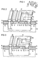
- Figure 2 and Figure 3 show a section through the center of the entrance protection structure with additional oblique view to the rear; the complete entrance protection structure tur is obtained by symmetrical continuation to the front.
- FIG. 1 there is a protective structure between an input 1 of an integrated circuit, in particular a bipolar integrated circuit, and a reference potential 2, in particular ground, which is provided by a transistor 3 with the coupling between base 16 and emitter 19 already explained, via a resistor 16a and is formed with a collector 11, 12 and by two integrated diodes 4, 5.
- the collector 11, 12 of the transistor 3 is connected to the input 1 and the connection point between the emitter 19 and the resistor 16a the reference potential 2 is connected.
- the two integrated diodes 4, 5 are also connected between the input 1 and the reference potential 2, the first diode 4 being connected directly in parallel to the emitter-collector path of the transistor 3. Due to the circuit polarities of the transistor 3 and the diodes 4, 5 resulting from FIG. 1, this protective structure acts for electrostatic discharges of both polarities.
- FIG. 1 The reference numerals according to FIG. 1, in particular for the transistor 3 and its connection through the resistor 16a, are chosen in accordance with the reference numerals according to FIG. 2 of the semiconductor system to be explained below, in which the protective structure is implemented according to a first exemplary embodiment.
- the protective structure in the semiconductor system according to FIG. 2 is explained below on the basis of the schematic process sequence during production.
- the starting point for the production of a semiconductor system according to FIG. 2 is a semiconductor substrate 10 of a first conductivity type, which is preferably the p-conductivity type.
- a particularly highly doped zone of the opposite second conduction type in this example the n-conduction type, is diffused into this semiconductor system by means of which a buried layer is produced using the subsequent production steps Zone 11 is formed.
- channel stopper regions 14 can be produced outside the buried layer zone 11, which have the first conduction type.
- An epitaxial layer 12 of the second conductivity type is then applied to the entire surface in a conventional manner.
- oxide zones 15, 15a, 15b are preferably formed such that they have at least the thickness of the epitaxial layer 12, so that the epitaxial layer 12 is completely interrupted by them at the locations of the semiconductor system which they cover. If this is not the case, the channel stopper regions 14 ensure complete isolation of the components from one another. In this way, the oxide zones 15 form part of an insulation frame to be completed around the entrance protection structure.
- the oxide zones 15a, 15b preferably extend through the epitaxial layer 12 into the underlying buried layer zone 11.
- a heavily doped zone 13 which in this example has the n-type conduction, is diffused through the epitaxial layer 12 into the buried layer zone 11.
- This contact zone 13 is advantageously designed such that it is laterally delimited by the oxide zones 15, 15a.
- Zones 16, 16a of the first conduction type here with p-conduction type, are now diffused into the n-doped epitaxial layer 12, which are in particular weakly doped.
- the zones 16 and 16a are isolated from one another at least by the oxide zone 15b. Because of the high layer resistance of the zones 16, 16a, the doping can also take place over the entire surface, ie without the use of a mask, without the heavily doped contact zone 13 is significantly changed.
- Zones 17 serve as contact zones for later connection of zone 16, and zones 17a, b accordingly serve as contact zones for zone 16a.
- a zone 19 of the second conductivity type here of the n conductivity type, is diffused into zone 16, the depth of which is dimensioned such that it is separated from the epitaxial layer 12 by the weakly doped zone 16.
- an insulation layer 18 consisting in particular of silicon oxide, which is either applied to the entire surface of the semiconductor system at this point in time or has already been produced in the preceding temperature steps of the diffusion processes, is structured in such a way that the contact zones 13, 17, 17b, 17a and Zone 19 can be connected.
- the zones mentioned are provided with interconnects 20, 21, 22, 23 as connections, the interconnect 20 being connected to the input 1 and the interconnect 22 being connected to the reference potential 2 (not shown).
- the interconnect 22 connects the zone 19 to the contact zone 17b, the interconnect 23 connects the contact zones 17 and 17a to one another.
- the interconnect 21 only serves to homogenize the potential profile in the zones 16, 17 and is not contacted to the outside.
- the parts of the insulation layer 18 located above the oxide zones 15 complete the already mentioned insulation frame 15, 18 around the entrance protection structure.
- an npn transistor 3 according to FIG. 1 is formed in the semiconductor system according to FIG. 1 by the buried layer zone 11 with the epitaxial layer 12 as collector, zone 16 as base, and zone 19 as emitter, the Zone 13 is the collector contact zone and zones 17 form the basic contact zones.
- the interconnect 20 as collector connection the transistor is connected with its collector 11, 12 to input 1 and via interconnect 22 as emitter connection with its emitter 19 to the reference potential.
- the resistor 16a is implemented by the weakly doped zone 16a. It is connected to the base contact zone 17 and thus to the base via the contact zone 17a and the interconnect 23 acting as a base connection, and to the emitter 19 via the contact zone 17b and the emitter connection 22. Of these interconnects 22, 23 apart from this, the resistor 16a is isolated from the base 16 and the emitter 19 by the oxide zones 15, 15b and parts of the insulation layer 18; By means of the part of the epitaxial layer 12 lying under the diffusion zone 16a, it forms with the buried layer zone 11 an integrated diode according to the diode 4 in FIG. 1 to be explained in more detail.
- the entrance protection structure according to FIG. 2 is to be completed towards the front by mirroring on the section line shown. Therefore, the complete input protection structure has a further resistor connected in parallel with the resistor 16a, i. That is, the resistor 16a shown in FIG. 1 is implemented in the semiconductor system by two resistors connected in parallel. This is particularly advantageous in view of the electrical properties of the input protection structure, which are yet to be explained.
- the first integrated diode 4 in FIG. 1 is formed in the semiconductor system according to FIG. 2 by the zone 16a and the underlying part of the epitaxial layer 12 including the buried layer zone 11. This first diode 4 is thus connected in parallel with the resistor 16a and the collector-base junction or in parallel with the emitter-collector path of the transistor and is arranged in a part of the epitaxial layer 12 which is essentially separate from the transistor region.
- the second integrated diode 5 is formed by the semiconductor substrate 10 and the buried layer zone 11, the semiconductor substrate 10 being connected to the reference potential 2 (not shown).
- FIG. 3 shows a further embodiment of the invention, the reference numbers being chosen in accordance with FIG. 2.
- this second embodiment differs from the first by the elimination of one of the two base contact zones 17 and the arrangement of the emitter terminal 22, which connects the resistor 16a to the emitter 19, and the base terminal 23, which the resistor 16a connects to the base contact zone 17 and thus the base 16.
- the rest of the structure and the process sequence for producing the protective structure according to FIG. 3 correspond to the protective structure according to FIG. 2.
- this second embodiment of the input protection structure also corresponds to the equivalent circuit diagram according to FIG. 1.
- a negative voltage pulse at input 1 is dissipated in part by the second protective diode 5 which is switched through. Another part flows to the reference potential 2 via the emitter connection 22, which at the same time represents the ground connection of the first protective diode 4.
- the first diode 4 is poled in the direction of flow.
- the protective structure works here in inverse transistor mode, the sensitive base-emitter junction being polarized in the reverse direction.
- the connection of the first diode 4 in a separate part of the epitaxial layer 12, essentially separated from the emitter-base region of the transistor 3 by the oxide insulation 15b, ensures a homogenization of the field strength and current profile and thus protects the sensitive side region of this transition.
- a positive voltage pulse switches the collector-base transition in the reverse direction and the base-emitter transition in the forward direction.
- a U CEO breakthrough would be the result. However, current can flow out of the base 16 via the resistor 16a, the protective structure changing over to the normal transistor mode of operation. The U CEO breakthrough turns into a U CER breakthrough through resistor 16a.
- the first integrated diode 4 connected between the emitter 19 and the collector 11, 12 in a separate part of the epitaxial layer 12 also has a positive effect here. Both the Collector-base transition of the npn transistor 3 and the first diode 4 are polarized in the reverse direction.
- the positive input pulse builds up on both barrier layers, wherein an excessive load on the side region of the collector-base transition opposite the collector connection 20 is avoided and a more uniform field strength distribution is achieved.
- the protective structure derives the voltage pulse due to its short switching time before components in parallel can be destroyed.
- the polarity of the sensitive base-emitter junction in the flow direction also guarantees that the component can withstand high loads.
- the arrangement of the connections and contact zones for the collector, base and emitter counteracts an excessive increase in the current density at the side region of the emitter-base junction opposite the collector connection 20. This advantage is particularly evident in the first embodiment according to FIG. 2. In contrast, the second embodiment according to FIG. 3 offers the advantage of a significantly smaller space requirement.
- the advantage of the protective structure presented is that it can be used for high signal voltages in the integrated circuit.
- the breakdown is determined by the U CER voltage, which is known to be greater than the U CEO voltage.
Description
Die vorliegende Erfindung betrifft eine Eingangsschutzstruktur für integrierte Schaltungen.The present invention relates to an input protection structure for integrated circuits.
Integrierte Schaltungen benötigen einen sicheren Schutz gegen elektrostatische Entladungen. Sich auf derartige elektrostatische Entladungen beziehende Mechanismen sind im einzelnen in der DE-OS 36 16 394 erläutert. Aus dieser Druckschrift ist insbesondere eine Eingangsschutzstruktur für bipolare integrierte Schaltungen bekannt, die aus einem zwischen einem Eingang und einem Referenzpotential geschalteten npn-Transistor besteht, dessen Basis über einen Widerstand gekoppelt (kurzgeschlossen) ist und auf Referenzpotential - speziell Masse - liegt.Integrated circuits require reliable protection against electrostatic discharge. Mechanisms relating to such electrostatic discharges are explained in detail in DE-OS 36 16 394. From this publication, in particular, an input protection structure for bipolar integrated circuits is known, which consists of an npn transistor connected between an input and a reference potential, the base of which is coupled (short-circuited) via a resistor and is at reference potential - especially ground.
Die technische Realisierung einer solchen Schutzstruktur in einem Halbleitersubstrat sieht einen üblichen Bipolartransistor in einer epitaktischen Schicht an der Oberfläche des Halbleitersubstrats vor, wobei der Kollektor dieses Transistors in üblicher Weise durch die hochohmige epitaktische Schicht und Basis sowie Emitter durch zwei entsprechende Diffusionsgebiete in der epitaktischen Schicht gebildet sind. Bei der üblichen Ausgestaltung des Transistors können aufgrund der erhöhten Ladungsträgerdichte in der Nähe der Systemoberfläche Oberflächenfrühdurchbrüche auftreten, wodurch die ESD-Belastbarkeit der Schutzstruktur vermindert werden kann.The technical implementation of such a protective structure in a semiconductor substrate provides for a conventional bipolar transistor in an epitaxial layer on the surface of the semiconductor substrate, the collector of this transistor being formed in the usual way by the high-resistance epitaxial layer and base and emitter by two corresponding diffusion regions in the epitaxial layer are. In the usual configuration of the transistor, surface breakthroughs can occur due to the increased charge carrier density in the vicinity of the system surface, as a result of which the ESD resistance of the protective structure can be reduced.
Eine weitere Eingangsschutzstruktur der in Rede stehenden Art ist in der europäischen Patentanmeldung EP-A-0 404 977 beschrieben. Diese ist jedoch auf die speziellen Anforderungen zugeschnitten, die bei einer großen Dicke der epitaktischen Schicht vorliegen, und nur bei bipolar integrierten Schaltungen mit einer Isolation benachbarter Bauelemente durch Diffusionsgebiete vorteilhaft zu realisieren.Another input protection structure of the type in question is described in European patent application EP-A-0 404 977. However, this is tailored to the special requirements that exist with a large thickness of the epitaxial layer, and can only be advantageously implemented in bipolar integrated circuits with insulation of adjacent components by diffusion regions.
Auch aus der Schrift "Patent Abstracts of Japan, Vol. 9, No. 193 (E-334) [1916], 9. August 1985 & JP-A-60 59762" ist eine Eingangsschutzstruktur bekannt, die einen Transistor und einen Widerstand besitzt, der extern mit der Basis und dem Emitter verbunden ist. Parallel zur Kollektor-Emitter-Strecke des Transistors ist eine Diode geschaltet, die durch den n-dotierten Kollektor und das p-dotierte Halbleitersubstrat gebildet ist. Allerdings sind dort der Transistor und der Widerstand in unterschiedlichen Wannen im Halbleitersubstrat ausgebildet.An input protection structure which has a transistor and a resistor is also known from the document "Patent Abstracts of Japan, Vol. 9, No. 193 (E-334) [1916], August 9, 1985 & JP-A-60 59762" which is externally connected to the base and the emitter. A diode, which is formed by the n-doped collector and the p-doped semiconductor substrate, is connected in parallel to the collector-emitter path of the transistor. However, the transistor and the resistor are formed in different wells in the semiconductor substrate.
Eine weitere Eingangsschutzstruktur mit einem Transistor und einem Widerstand ist aus der Schrift "Patent Abstracts of Japan, Vol. 5, No. 145 (E-74) [817], 12. September 1981 & JP-A-56 79463" bekannt, wobei auch dort der Kollektor-Emitter-Strecke eine Diode parallel geschaltet ist. Wie aus Figur 4 dieser Schrift hervorgeht, wird die Diode ebenfalls durch das Halbleitersubstrat und die Kollektorzone gebildet.Another input protection structure with a transistor and a resistor is known from the document "Patent Abstracts of Japan, Vol. 5, No. 145 (E-74) [817], September 12, 1981 & JP-A-56 79463", wherein there too, a diode is connected in parallel to the collector-emitter path. As can be seen from Figure 4 of this document, the diode is also formed by the semiconductor substrate and the collector zone.
Die US-A-4 486 770 beschreibt eine Eingangsschutzstruktur mit einem Transistor und einem Widerstand. Dabei stellt der Widerstand jedoch ein mit der Basis zusammenhängendes dotiertes Gebiet dar. Eine externe Verbindung über eine Leitbahn ist nur mit dem Emitter, nicht jedoch mit der Basis vorgesehen. Ferner hängt die vergrabene hochdotierte Schicht 40 (buried collector) unter der Basis nur über eine schmale Stelle mit derjenigen unterhalb des Widerstandes zusammen.US-A-4 486 770 describes an input protection structure with a transistor and a resistor. However, the resistance represents a doped area connected to the base. An external connection A track is provided only with the emitter, but not with the base. Furthermore, the buried, highly doped layer 40 (buried collector) under the base is only connected to that below the resistor via a narrow point.
Der vorliegenden Erfindung liegt daher die Aufgabe zugrunde, eine Eingangsschutzstruktur der in Rede stehenden Art anzugeben, die bei bipolaren integrierten Schaltungen mit einer Isolation benachbarter Bauelemente durch Oxidgebiete einen zuverlässigen Schutz bei einer einfachen Herstellungsweise gewährleistet.The present invention is therefore based on the object of specifying an input protection structure of the type in question which, in the case of bipolar integrated circuits with isolation of adjacent components by oxide regions, ensures reliable protection with a simple production method.
Diese Aufgabe wird bei einer Eingangsschutzstruktur der eingangs genannten Art erfindungsgemäß durch die Merkmale des Patentanspruchs 1 gelöst. Weiterbildungen der Erfindung sind Gegenstand von Unteransprüchen.This object is achieved according to the invention in an input protection structure of the type mentioned at the outset by the features of patent claim 1. Developments of the invention are the subject of dependent claims.
Die Erfindung wird im folgenden anhand von Ausführungsbeispielen gemäß den Figuren 1 bis 3 der Zeichnung näher erläutert. Es zeigt:
- Figur 1
- ein Ersatzschaltbild einer Eingangsschutzstruktur in Form eines Transistors mit einem Widerstand und zweier integrierter Dioden,
Figur 2 undFigur 3- zwei Ausführungsformen der Realisierung einer Eingangsschutzstruktur nach Figur 1 in einem Halbleitersystem in schematischer Darstellung.
- Figure 1
- an equivalent circuit diagram of an input protection structure in the form of a transistor with a resistor and two integrated diodes,
- Figure 2 and Figure 3
- Two embodiments of the implementation of an input protection structure according to Figure 1 in a semiconductor system in a schematic representation.
Figur 2 und Figur 3 zeigen dabei einen Schnitt durch die Mitte der Eingangsschutzstruktur mit zusätzlicher Schrägaufsicht nach hinten; die vollständige Eingangsschutzstruk tur erhält man durch symmetrische Fortsetzung nach vorne.Figure 2 and Figure 3 show a section through the center of the entrance protection structure with additional oblique view to the rear; the complete entrance protection structure tur is obtained by symmetrical continuation to the front.
Gemäß Figur 1 liegt zwischen einem Eingang 1 einer integrierten Schaltung, insbesondere einer bipolaren integrierten Schaltung, und einem Referenzpotential 2, insbesondere Masse, eine Schutzstruktur, welche durch einen Transistor 3 mit der bereits erläuterten Kopplung zwischen Basis 16 und Emitter 19 über einen Widerstand 16a und mit einem Kollektor 11, 12 und durch zwei integrierte Dioden 4, 5 gebildet ist. Insbesondere ist dabei der Kollektor 11, 12 des Transistors 3 an den Eingang 1 und der Verbindungspunkt zwischen Emitter 19 und Widerstand 16a an das Bezugspotential 2 angeschlossen. Die beiden integrierten Dioden 4, 5 sind ebenfalls zwischen den Eingang 1 und das Referenzpotential 2 geschaltet, wobei die erste Diode 4 direkt parallel zur Emitter-Kollektor-Strecke des Transistors 3 geschaltet ist. Aufgrund der sich aus Figur 1 ergebenden Schaltungspolaritäten des Transistors 3 und der Dioden 4, 5 wirkt diese Schutzstruktur für elektrostatische Entladungen beider Polaritäten.According to FIG. 1, there is a protective structure between an input 1 of an integrated circuit, in particular a bipolar integrated circuit, and a
Die Bezugszeichen nach Figur 1, insbesondere für den Transistor 3 und dessen Beschaltung durch den Widerstand 16a sind in Übereinstimmung mit den Bezugszeichen nach Figur 2 des im folgenden zu erläuternden Halbleitersystems gewählt, in dem die Schutzstruktur gemäß eines ersten Ausführungsbeispiels realisiert ist. Die Schutzstruktur im Halbleitersystem nach Figur 2 wird im folgenden anhand der schematischen Verfahrensabfolge bei der Herstellung erläutert.The reference numerals according to FIG. 1, in particular for the
Ausgangspunkt für die Herstellung eines Halbleitersystems nach Figur 2 ist ein Halbleitersubstrat 10 eines ersten Leitungstyps, bei dem es sich vorzugsweise um den p-Leitungstyp handelt. In dieses Halbleitersystem wird in an sich konventioneller Weise, beispielsweise durch eine Implantation mit einem anschließenden Temperaturschritt, zunächst eine insbesondere hochdotierte Zone des entgegengesetzten zweiten Leitungstyps, im vorliegenden Beispiel also des n-Leitungstyps, eindiffundiert, durch die mit den nachfolgenden Herstellungsschritten eine Buried-Layer-Zone 11 gebildet wird. Um die Wirkungsweise eines später zu bildenden Isolationsrahmens um die Schutzstruktur herum zu verbessern, können bekanntlich sogenannte Channel-Stopper-Bereiche 14 außerhalb der Buried-Layer-Zone 11 hergestellt werden, die den ersten Leitungstyp aufweisen. Anschließend wird in üblicher Weise eine epitaktische Schicht 12 des zweiten Leitungstyps auf die gesamte Oberfläche aufgebracht.The starting point for the production of a semiconductor system according to FIG. 2 is a
Zur Isolation verschiedener Teile der Schutzstruktur untereinander einerseits und der gesamten Struktur von benachbarten Gebieten des Halbleitersystems andererseits wird nun vorzugsweise eine konventionelle LOCOS-Technik angewandt. Derartige Isolationstechniken sind in dem Buch von D. Widmann, H. Mahrer, H. Friedrich, Technologie hochintegrierter Schaltungen, Springer-Verlag 1988, Seite 67 bis 72, erläutert. Es wird eine geeignete Maske (nicht dargestellt) aufgebracht, mit deren Hilfe zunächst in die epitaktische Schicht 12 Vertiefungen von etwa der halben Schichtdicke der epitaktischen Schicht geätzt werden, anschließend werden diese Stellen lokal aufoxidiert. Bevorzugt werden dabei solche LOCOS-Techniken eingesetzt, die zu Oxidzonen 15, 15a, 15b mit ebener Oberfläche führen. Alternativ kann auch eine Grabenisolationstechnik, wie sie in derselben Literaturstelle auf Seite 78 beschrieben ist, eingesetzt werden, die dann ebenfalls zu Oxidzonen 15, 15a, 15b führt. Die Oxidzonen 15, 15a, 15b werden vorzugsweise so ausgebildet, daß sie mindestens die Dicke der epitaktischen Schicht 12 besitzen, so daß an den von ihnen bedeckten Stellen des Halbleitersystems die epitaktische Schicht 12 durch sie vollständig unterbrochen wird. Ist das nicht der Fall, sorgen die Channel-Stopper-Bereiche 14 für eine vollständige Isolation der Bauelemente untereinander. Die Oxidzonen 15 bilden auf diese Weise einen Teil eines noch zu vervollständigen Isolationsrahmens um die Eingangsschutzstruktur herum. Die Oxidzonen 15a, 15b reichen vorzugsweise durch die epitaktische Schicht 12 bis in die unterliegende Buried-Layer-Zone 11 hinein.Conventional LOCOS technology is now preferably used to isolate different parts of the protective structure from one another and from the entire structure of adjacent areas of the semiconductor system. Such isolation techniques are explained in the book by D. Widmann, H. Mahrer, H. Friedrich, Technologie hochintegrierter Schaltungen, Springer-Verlag 1988, pages 67 to 72. A suitable mask (not shown) is applied, with the aid of which depressions of approximately half the layer thickness of the epitaxial layer are first etched into the
Für die niederohmige Kontaktierung der Buried-Layer-Zone 11 mit einem noch zu bildenden Anschluß wird eine hochdotierte Zone 13, die in diesem Beispiel den n-Leitungstyp aufweist, durch die epitaktische Schicht 12 in die Buried-Layer-Zone 11 eindiffundiert. Vorteilhafterweise wird diese Kontaktzone 13 so ausgebildet, daß sie seitlich durch die Oxidzonen 15, 15a begrenzt wird.For the low-resistance contacting of the buried
In die hier n-dotierte epitaktische Schicht 12 werden nun Zonen 16, 16a des ersten Leitungstyps, hier also mit p-Leitungstyp, eindiffundiert, die insbesondere schwach dotiert sind. An der Oberfläche des Halbleitersubstrats 10 bzw. der epitaktischen Schicht 12 sind die Zonen 16 und 16a mindestens durch die Oxidzone 15b voneinander isoliert. Aufgrund des hohen Schichtwiderstands der Zonen 16, 16a kann die Dotierung auch ganzflächig, d. h. ohne Einsatz einer Maske, erfolgen, ohne daß dabei die hochdotierte Kontaktzone 13 nennenswert verändert wird.
In die Zone 16 werden nun hochdotierte Teilzonen 17 und gleichzeitig in die Zone 16a hochdotierte Teilzonen 17a, 17b desselben Leitungstyps wie die Zonen 16 und 16a, im vorliegenden Fall also des p-Leitungstyps, eindiffundiert. Dabei dienen die Zonen 17 als Kontaktzonen für einen späteren Anschluß der Zone 16, und entsprechend die Zonen 17a, b als Kontaktzonen für die Zone 16a.Highly doped
Nachfolgend wird in die Zone 16 eine Zone 19 des zweiten Leitungstyps, hier also des n-Leitungstyps, eindiffundiert, deren Tiefe so bemessen wird, daß sie von der epitaktischen Schicht 12 durch die schwach dotierte Zone 16 getrennt ist. Schließlich wird eine insbesondere aus Siliziumoxid bestehende Isolationsschicht 18, die entweder zu diesem Zeitpunkt auf die gesamte Oberfläche des Halbleitersystems aufgebracht wird oder bei den vorausgegangenen Temperaturschritten der Diffusionsprozesse bereits erzeugt worden ist, so strukturiert, daß die Kontaktzonen 13, 17, 17b, 17a und die Zone 19 anschließbar sind. Die erwähnten Zonen werden mit Leitbahnen 20, 21, 22, 23 als Anschlüsse versehen, wobei die Leitbahn 20 mit dem Eingang 1 und die Leitbahn 22 mit dem Referenzpotential 2 verbunden werden (nicht dargestellt). Die Leitbahn 22 verbindet die Zone 19 mit der Kontaktzone 17b, die Leitbahn 23 verbindet die Kontaktzonen 17 und 17a miteinander. Die Leitbahn 21 dient lediglich der Homogenisierung des Potentialverlaufs in den Zonen 16, 17 und wird nicht nach außen kontaktiert.Subsequently, a
Die oberhalb der Oxidzonen 15 befindlichen Teile der Isolationsschicht 18 vervollständigen den bereits erwähnten Isolationsrahmen 15, 18 um die Eingangsschutzstruktur herum.The parts of the
Aufgrund der erläuterten Zonenstruktur wird im Halbleitersystem nach Figur 2 ein npn-Transistor 3 gemäß Figur 1 gebildet durch die Buried-Layer-Zone 11 mit der epitaktischen Schicht 12 als Kollektor, die Zone 16 als Basis, und die Zone 19 als Emitter, wobei die Zone 13 die Kollektor-Kontaktzone und die Zonen 17 die Basis-Kontaktzonen bilden. Über die Leitbahn 20 als Kollektor-Anschluß wird der Transistor mit seinem Kollektor 11, 12 an den Eingang 1 und über die Leitbahn 22 als Emitter-Anschluß mit seinem Emitter 19 an das Referenzpotential geschaltet.Based on the zone structure explained, an
Erfindungsgemäß wird der Widerstand 16a durch die schwach dotierte Zone 16a realisiert. Er ist über die Kontaktzone 17a und die als Basis-Anschluß wirkende Leitbahn 23 an die Basis-Kontaktzone 17 und damit an die Basis angeschlossen, sowie über die Kontaktzone 17b und den Emitter-Anschluß 22 an den Emitter 19. Von diesen Leitbahnen 22, 23 abgesehen ist der Widerstand 16a durch die Oxidzonen 15, 15b und Teile der Isolationsschicht 18 von der Basis 16 und dem Emitter 19 isoliert; mittels des unter der Diffusionszone 16a liegenden Teils der epitaktischen Schicht 12 bildet er mit der Buried-Layer-Zone 11 eine noch genauer zu erläuternde integrierte Diode gemäß der Diode 4 in Figur 1.According to the invention, the
Wie bereits angegeben, ist die Eingangsschutzstruktur nach Figur 2 durch Spiegelung an der dargestellten Schnittlinie nach vorne hin zu vervollständigen. Daher weist die komplette Eingangsschutzstruktur einen zum Widerstand 16a parallel geschalteten weiteren Widerstand auf, d. h., der in Figur 1 dargestellte Widerstand 16a wird im Halbleitersystem durch zwei parallel geschaltete Widerstände realisiert. Dies ist im Hinblick auf die noch zu erläuternden elektrischen Eigenschaften der Eingangsschutzstruktur besonders vorteilhaft.As already stated, the entrance protection structure according to FIG. 2 is to be completed towards the front by mirroring on the section line shown. Therefore, the complete input protection structure has a further resistor connected in parallel with the
Die erste integrierte Diode 4 in Figur 1 wird im Halbleitersystem nach Figur 2 durch die Zone 16a und den unterliegenden Teil der epitaktischen Schicht 12 einschließlich der Buried-Layer-Zone 11 gebildet. Diese erste Diode 4 ist somit parallel zum Widerstand 16a und zum Kollektor-Basis-Übergang bzw. parallel zur Emitter-Kollektor-Strecke des Transistors geschaltet und in einem vom Transistor-Bereich im wesentlichen getrennten Teil der epitaktischen Schicht 12 angeordnet. Die zweite integrierte Diode 5 wird durch das Halbleitersubstrat 10 und die Buried-Layer-Zone 11 gebildet, wobei das Halbleitersubstrat 10 an das Referenzpotential 2 anzuschließen ist (nicht dargestellt).The first integrated diode 4 in FIG. 1 is formed in the semiconductor system according to FIG. 2 by the
Figur 3 zeigt eine weitere Ausführungsform der Erfindung, wobei die Bezugsziffern in Übereinstimmung mit Figur 2 gewählt sind. Ersichtlich unterscheidet sich diese zweite Ausführungsform von der ersten durch den Wegfall einer der beiden Basis-Kontakt-Zonen 17 und die Anordnung des Emitter-Anschlusses 22, der den Widerstand 16a mit dem Emitter 19 verbindet, und des Basis-Anschlusses 23, der den Widerstand 16a mit der Basis-Kontaktzone 17 und damit der Basis 16 verbindet. Der übrige Aufbau und der Verfahrensablauf zur Herstellung der Schutzstruktur nach Figur 3 stimmt mit der Schutzstruktur nach Figur 2 überein. Insbesondere entspricht auch diese zweite Ausführungsform der Eingangsschutzstruktur dem Ersatzschaltbild nach Figur 1.FIG. 3 shows a further embodiment of the invention, the reference numbers being chosen in accordance with FIG. 2. Obviously, this second embodiment differs from the first by the elimination of one of the two
Ein negativer Spannungsimpuls am Eingang 1 wird zum Teil durch die in Durchlaß geschaltete zweite Schutzdiode 5 abgeführt. Ein anderer Teil fließt über den Emitter-Anschluß 22, der gleichzeitig den Masseanschluß der ersten Schutzdiode 4 darstellt, zum Referenzpotential 2 ab. Die erste Diode 4 ist in Flußrichtung gepolt. Die Schutzstruktur arbeitet hier im inversen Transistorbetrieb, wobei der empfindliche Basis-Emitter-Übergang in Sperrichtung gepolt ist. Der Anschluß der ersten Diode 4 in einem separaten Teil der epitaktischen Schicht 12, im wesentlichen getrennt vom Emitter-Basis-Bereich des Transistors 3 durch die Oxidisolation 15b, sorgt für eine Homogenisierung des Feldstärke-und Stromverlaufs und schützt so den empfindlichen Seitenbereichs dieses Übergangs.A negative voltage pulse at input 1 is dissipated in part by the second protective diode 5 which is switched through. Another part flows to the
Ein positiver Spannungsimpuls schaltet den Kollektor-Basis-Übergang in Sperrichtung sowie den Basis-Emitter-Übergang in Durchlaßrichtung. Ein UCEO-Durchbruch wäre die Folge. Über den Widerstand 16a kann jedoch ein Stromfluß aus der Basis 16 erfolgen, wobei die Schutzstruktur in die normale Transistorarbeitsweise übergeht. Der UCEO-Durchbruch geht durch den Widerstand 16a in einen UCER-Durchbruch über. Die zwischen Emitter 19 und Kollektor 11,12 geschaltete erste integrierte Diode 4 in einem separaten Teil der epitaktischen Schicht 12 macht sich hier ebenfalls positiv bemerkbar. Sowohl der Kollektor-Basis-Übergang des npn-Transistors 3 als auch die erste Diode 4 sind in Sperrichtung gepolt. Der positive Eingangsimpuls baut sich an beiden Sperrschichten auf, wobei eine zu starke Belastung des dem Kollektor-Anschluß 20 gegenüberliegenden Seitenbereich des Kollektor-Basis-Übergangs vermieden wird und eine gleichmäßigere Feldstärke-Verteilung erreicht wird. Die Schutzstruktur leitet den Spannungsimpuls auf Grund ihrer kurzen Durchschaltzeit ab, bevor parallel liegende Baueelemente zerstört werden können. Die Polung des empfindlichen Basis-Emitter-Übergangs in Durchflußrichtung garantiert zudem eine hohe Belastbarkeit des Bauelements.A positive voltage pulse switches the collector-base transition in the reverse direction and the base-emitter transition in the forward direction. A U CEO breakthrough would be the result. However, current can flow out of the
Durch die Anordnung der Anschlüsse und Kontaktzonen für Kollektor, Basis und Emitter wird einer zu großen Erhöhung der Stromdichte an dem dem Kollektor-Anschluß 20 gegenüberliegenden Seitenbereich des Emitter-Basis-Überganges entgegengewirkt. Dieser Vorteil kommt insbesondere bei der ersten Ausführungsform gemäß Figur 2 zum Tragen. Die zweite Ausführungsform gemäß Figur 3 bietet dagegen den Vorteil eines deutlich geringeren Platzbedarfs.The arrangement of the connections and contact zones for the collector, base and emitter counteracts an excessive increase in the current density at the side region of the emitter-base junction opposite the
Der Vorteil der vorgestellten Schutzstruktur liegt in der Verwendungsmöglichkeit für hohe Signalspannungen des integrierten Schaltkreises. Der Durchbruch wird bestimmt durch die UCER-Spannung, welche bekanntlich größer ist als die UCEO-Spannung.The advantage of the protective structure presented is that it can be used for high signal voltages in the integrated circuit. The breakdown is determined by the U CER voltage, which is known to be greater than the U CEO voltage.
Claims (4)
- Input protection structure for bipolar integrated circuits, which- is disposed between an input (1) and a reference potential (2), and- has at least one transistor (3) with a resistor (16a),-- whose collector (11) is connected to the input (1) and whose base (16) is connected via the resistor (16a) and jointly with its emitter (19) to the reference potential (2),-- the collector (11) being formed in a semiconductor substrate (10) of a first conduction type as a buried collector by means of a zone of a second conduction type,-- the base (16) being formed by at least one doped zone of the first conduction type in an epitaxial layer (12) of the second conduction type applied to the semiconductor substrate (10) above and in contact with the buried collector (11) and being provided with a base terminal (23) formed as a conductor track,-- the collector (11) being provided with a collector terminal (20) formed as a conductor track by means of a contact zone (13) of the second conduction type which extends through the epitaxial layer (12),-- the emitter (19) furthermore being formed by a doped zone of the second conduction type in the base zone (16) and being provided with an emitter terminal (22) formed as a conductor track, and-- the resistor (16a) being formed by at least one further lightly doped zone (16a) of the first conduction type in the epitaxial layer (12), which layer is connected at one end to the emitter (19) only via the emitter terminal (22) and at the other end to the base (16) only via the base terminal (23) and being isolated from the base zone or zones (16, 17) by an oxide zone (15b) which is at least as thick as the epitaxial layer (12),- and has a first integrated diode (4) which is formed by the further lightly doped zone (16a) of the first conduction type and the part situated underneath it of the epitaxial layer (12), including a part of the buried collector (11), and it also has a second integrated diode (5) which is formed by the semiconductor substrate (10) connected to the reference potential and the buried collector (11).
- Input protection structure according to Claim 1, in which the resistor (16a) is made up of two parallel-connected resistors having essentially equal resistance values, the two parallel-connected resistors being formed by the further lightly doped zone and an additional lightly doped zone of the first conduction type in a symmetrical manner with respect to one another.
- Input protection structure according to one of Claims 1 or 2, in which the base (16) comprises a lightly doped zone (16) having at least one heavily doped subzone (17) as base contact zone.
- Input protection structure according to Claim 3, in which the lightly doped zone forming the resistor (16a) has, at its ends, two heavily doped subzones (17a, 17b), produced simultaneously with the base contact zones (17) as contact zones and is connected via one of said subzones (17a) to the base terminal (23) and via the other subzone (17b) to the emitter terminal (22).
Priority Applications (4)
| Application Number | Priority Date | Filing Date | Title |
|---|---|---|---|
| DE58908843T DE58908843D1 (en) | 1989-10-30 | 1989-10-30 | Input protection structure for integrated circuits. |
| EP89120144A EP0429686B1 (en) | 1989-10-30 | 1989-10-30 | Input protection structure for integrated circuits |
| US07/606,036 US5187562A (en) | 1989-10-30 | 1990-10-30 | Input protection structure for integrated circuits |
| JP29517390A JP3193368B2 (en) | 1989-10-30 | 1990-10-30 | Integrated circuit input terminal protection circuit |
Applications Claiming Priority (1)
| Application Number | Priority Date | Filing Date | Title |
|---|---|---|---|
| EP89120144A EP0429686B1 (en) | 1989-10-30 | 1989-10-30 | Input protection structure for integrated circuits |
Publications (2)
| Publication Number | Publication Date |
|---|---|
| EP0429686A1 EP0429686A1 (en) | 1991-06-05 |
| EP0429686B1 true EP0429686B1 (en) | 1994-12-28 |
Family
ID=8202078
Family Applications (1)
| Application Number | Title | Priority Date | Filing Date |
|---|---|---|---|
| EP89120144A Expired - Lifetime EP0429686B1 (en) | 1989-10-30 | 1989-10-30 | Input protection structure for integrated circuits |
Country Status (4)
| Country | Link |
|---|---|
| US (1) | US5187562A (en) |
| EP (1) | EP0429686B1 (en) |
| JP (1) | JP3193368B2 (en) |
| DE (1) | DE58908843D1 (en) |
Families Citing this family (3)
| Publication number | Priority date | Publication date | Assignee | Title |
|---|---|---|---|---|
| JP4506424B2 (en) * | 2004-11-18 | 2010-07-21 | トヨタ自動車株式会社 | Protection circuit |
| US8350352B2 (en) * | 2009-11-02 | 2013-01-08 | Analog Devices, Inc. | Bipolar transistor |
| JP6705726B2 (en) * | 2016-09-14 | 2020-06-03 | ルネサスエレクトロニクス株式会社 | Semiconductor device |
Family Cites Families (11)
| Publication number | Priority date | Publication date | Assignee | Title |
|---|---|---|---|---|
| JPS5469391A (en) * | 1977-11-14 | 1979-06-04 | Nec Corp | Integrated composite element |
| US4228451A (en) * | 1978-07-21 | 1980-10-14 | Monolithic Memories, Inc. | High resistivity semiconductor resistor device |
| US4264941A (en) * | 1979-02-14 | 1981-04-28 | National Semiconductor Corporation | Protective circuit for insulated gate field effect transistor integrated circuits |
| JPS5679463A (en) * | 1979-12-03 | 1981-06-30 | Matsushita Electronics Corp | Semiconductor integrated circuit |
| JPS56104465A (en) * | 1980-01-25 | 1981-08-20 | Hitachi Ltd | Semiconductor device |
| JPS5734361A (en) * | 1980-08-11 | 1982-02-24 | Toshiba Corp | Semiconductor device |
| US4486770A (en) * | 1981-04-27 | 1984-12-04 | General Motors Corporation | Isolated integrated circuit transistor with transient protection |
| JPS5812343A (en) * | 1981-07-15 | 1983-01-24 | Nec Corp | Semiconductor device |
| IT1221867B (en) * | 1983-05-16 | 1990-07-12 | Ates Componenti Elettron | STRUCTURE OF BIPOLAR POWER TRANSISTOR WITH BASIC INCORPORATED BY-PASSABLE BALANCING RESISTANCE |
| JPS6059762A (en) * | 1983-09-13 | 1985-04-06 | Nec Corp | Electrostatic protecting circuit |
| IT1217298B (en) * | 1985-05-30 | 1990-03-22 | Sgs Thomson Microelectronics | ELECTROSTATIC DISCHARGE PROTECTION DEVICE, IN PARTICULAR FOR BIPOLAR INTEGRATED CIRCUITS |
-
1989
- 1989-10-30 DE DE58908843T patent/DE58908843D1/en not_active Expired - Lifetime
- 1989-10-30 EP EP89120144A patent/EP0429686B1/en not_active Expired - Lifetime
-
1990
- 1990-10-30 JP JP29517390A patent/JP3193368B2/en not_active Expired - Fee Related
- 1990-10-30 US US07/606,036 patent/US5187562A/en not_active Expired - Lifetime
Also Published As
| Publication number | Publication date |
|---|---|
| US5187562A (en) | 1993-02-16 |
| DE58908843D1 (en) | 1995-02-09 |
| EP0429686A1 (en) | 1991-06-05 |
| JP3193368B2 (en) | 2001-07-30 |
| JPH03154374A (en) | 1991-07-02 |
Similar Documents
| Publication | Publication Date | Title |
|---|---|---|
| DE2257846C3 (en) | Integrated semiconductor arrangement for protection against overvoltage | |
| EP1019964B1 (en) | Integrated circuit with semiconductor comprising a structure for protection against electrostatic discharges | |
| DE3834841C2 (en) | Integrated arrangement in a substrate to avoid parasitic substrate effects | |
| DE3203066A1 (en) | SEMICONDUCTOR COMPONENT | |
| DE3533478C2 (en) | Monolithically integrated semiconductor power device | |
| DE69635885T2 (en) | Circuit with a protective agent | |
| EP0000169B1 (en) | Semiconductor junction capacitor in integrated method of construction and bootstrap circuit with such a capacitor | |
| EP0307850B1 (en) | Si/SiGe semiconductor body | |
| EP0098496A1 (en) | IGFET with injector zone | |
| DE19647398B4 (en) | Bipolar transistor with insulated gate | |
| EP0000909B1 (en) | Lateral transistor | |
| DE2531249A1 (en) | MULTILAYER THYRISTOR | |
| EP0429686B1 (en) | Input protection structure for integrated circuits | |
| DE3103785A1 (en) | SEMICONDUCTOR ARRANGEMENT WITH HIGH BREAKTHROUGH VOLTAGE | |
| EP0413054B1 (en) | Input protection structure for integrated circuits | |
| DE69834451T2 (en) | Protection device for an integrated MOS transistor sufficient voltage gradient | |
| EP0414934B1 (en) | Input protection structure for integrated circuits | |
| EP0442064B1 (en) | Input protection structure for integrated circuits | |
| DE2357332A1 (en) | INTEGRATED CIRCUIT | |
| EP0477393B1 (en) | Input protection structure for integrated circuits | |
| EP0404977B1 (en) | Input protection structure for integrated circuits | |
| EP0092671A2 (en) | Transistor for integrated circuits | |
| DE3835569C2 (en) | ||
| EP0443055A1 (en) | Input protection structure for integrated circuits | |
| DE3632642A1 (en) | SEMICONDUCTOR PERFORMANCE COMPONENT |
Legal Events
| Date | Code | Title | Description |
|---|---|---|---|
| PUAI | Public reference made under article 153(3) epc to a published international application that has entered the european phase |
Free format text: ORIGINAL CODE: 0009012 |
|
| AK | Designated contracting states |
Kind code of ref document: A1 Designated state(s): AT BE CH DE ES FR GB GR IT LI LU NL SE |
|
| 17P | Request for examination filed |
Effective date: 19910917 |
|
| 17Q | First examination report despatched |
Effective date: 19930225 |
|
| RBV | Designated contracting states (corrected) |
Designated state(s): DE FR GB IT NL |
|
| GRAA | (expected) grant |
Free format text: ORIGINAL CODE: 0009210 |
|
| AK | Designated contracting states |
Kind code of ref document: B1 Designated state(s): DE FR GB IT NL |
|
| REF | Corresponds to: |
Ref document number: 58908843 Country of ref document: DE Date of ref document: 19950209 |
|
| ITF | It: translation for a ep patent filed |
Owner name: STUDIO JAUMANN |
|
| GBT | Gb: translation of ep patent filed (gb section 77(6)(a)/1977) |
Effective date: 19950303 |
|
| ET | Fr: translation filed | ||
| PLBE | No opposition filed within time limit |
Free format text: ORIGINAL CODE: 0009261 |
|
| STAA | Information on the status of an ep patent application or granted ep patent |
Free format text: STATUS: NO OPPOSITION FILED WITHIN TIME LIMIT |
|
| 26N | No opposition filed | ||
| REG | Reference to a national code |
Ref country code: GB Ref legal event code: IF02 |
|
| PGFP | Annual fee paid to national office [announced via postgrant information from national office to epo] |
Ref country code: GB Payment date: 20030929 Year of fee payment: 15 |
|
| PGFP | Annual fee paid to national office [announced via postgrant information from national office to epo] |
Ref country code: NL Payment date: 20030930 Year of fee payment: 15 |
|
| PG25 | Lapsed in a contracting state [announced via postgrant information from national office to epo] |
Ref country code: GB Free format text: LAPSE BECAUSE OF NON-PAYMENT OF DUE FEES Effective date: 20041030 |
|
| PG25 | Lapsed in a contracting state [announced via postgrant information from national office to epo] |
Ref country code: NL Free format text: LAPSE BECAUSE OF NON-PAYMENT OF DUE FEES Effective date: 20050501 |
|
| GBPC | Gb: european patent ceased through non-payment of renewal fee |
Effective date: 20041030 |
|
| NLV4 | Nl: lapsed or anulled due to non-payment of the annual fee |
Effective date: 20050501 |
|
| PG25 | Lapsed in a contracting state [announced via postgrant information from national office to epo] |
Ref country code: IT Free format text: LAPSE BECAUSE OF NON-PAYMENT OF DUE FEES;WARNING: LAPSES OF ITALIAN PATENTS WITH EFFECTIVE DATE BEFORE 2007 MAY HAVE OCCURRED AT ANY TIME BEFORE 2007. THE CORRECT EFFECTIVE DATE MAY BE DIFFERENT FROM THE ONE RECORDED. Effective date: 20051030 |
|
| PGFP | Annual fee paid to national office [announced via postgrant information from national office to epo] |
Ref country code: FR Payment date: 20081014 Year of fee payment: 20 |
|
| PGFP | Annual fee paid to national office [announced via postgrant information from national office to epo] |
Ref country code: DE Payment date: 20081216 Year of fee payment: 20 |