JP6705726B2 - Semiconductor device - Google Patents
Semiconductor device Download PDFInfo
- Publication number
- JP6705726B2 JP6705726B2 JP2016179331A JP2016179331A JP6705726B2 JP 6705726 B2 JP6705726 B2 JP 6705726B2 JP 2016179331 A JP2016179331 A JP 2016179331A JP 2016179331 A JP2016179331 A JP 2016179331A JP 6705726 B2 JP6705726 B2 JP 6705726B2
- Authority
- JP
- Japan
- Prior art keywords
- region
- semiconductor
- semiconductor device
- semiconductor region
- epitaxial layer
- Prior art date
- Legal status (The legal status is an assumption and is not a legal conclusion. Google has not performed a legal analysis and makes no representation as to the accuracy of the status listed.)
- Active
Links
Images


Classifications
-
- H—ELECTRICITY
- H01—ELECTRIC ELEMENTS
- H01L—SEMICONDUCTOR DEVICES NOT COVERED BY CLASS H10
- H01L27/00—Devices consisting of a plurality of semiconductor or other solid-state components formed in or on a common substrate
- H01L27/02—Devices consisting of a plurality of semiconductor or other solid-state components formed in or on a common substrate including semiconductor components specially adapted for rectifying, oscillating, amplifying or switching and having at least one potential-jump barrier or surface barrier; including integrated passive circuit elements with at least one potential-jump barrier or surface barrier
- H01L27/0203—Particular design considerations for integrated circuits
- H01L27/0248—Particular design considerations for integrated circuits for electrical or thermal protection, e.g. electrostatic discharge [ESD] protection
- H01L27/0251—Particular design considerations for integrated circuits for electrical or thermal protection, e.g. electrostatic discharge [ESD] protection for MOS devices
- H01L27/0255—Particular design considerations for integrated circuits for electrical or thermal protection, e.g. electrostatic discharge [ESD] protection for MOS devices using diodes as protective elements
-
- H—ELECTRICITY
- H01—ELECTRIC ELEMENTS
- H01L—SEMICONDUCTOR DEVICES NOT COVERED BY CLASS H10
- H01L27/00—Devices consisting of a plurality of semiconductor or other solid-state components formed in or on a common substrate
- H01L27/02—Devices consisting of a plurality of semiconductor or other solid-state components formed in or on a common substrate including semiconductor components specially adapted for rectifying, oscillating, amplifying or switching and having at least one potential-jump barrier or surface barrier; including integrated passive circuit elements with at least one potential-jump barrier or surface barrier
- H01L27/0203—Particular design considerations for integrated circuits
- H01L27/0248—Particular design considerations for integrated circuits for electrical or thermal protection, e.g. electrostatic discharge [ESD] protection
- H01L27/0251—Particular design considerations for integrated circuits for electrical or thermal protection, e.g. electrostatic discharge [ESD] protection for MOS devices
- H01L27/0288—Particular design considerations for integrated circuits for electrical or thermal protection, e.g. electrostatic discharge [ESD] protection for MOS devices using passive elements as protective elements, e.g. resistors, capacitors, inductors, spark-gaps
-
- H—ELECTRICITY
- H01—ELECTRIC ELEMENTS
- H01L—SEMICONDUCTOR DEVICES NOT COVERED BY CLASS H10
- H01L23/00—Details of semiconductor or other solid state devices
- H01L23/52—Arrangements for conducting electric current within the device in operation from one component to another, i.e. interconnections, e.g. wires, lead frames
- H01L23/535—Arrangements for conducting electric current within the device in operation from one component to another, i.e. interconnections, e.g. wires, lead frames including internal interconnections, e.g. cross-under constructions
-
- H—ELECTRICITY
- H01—ELECTRIC ELEMENTS
- H01L—SEMICONDUCTOR DEVICES NOT COVERED BY CLASS H10
- H01L27/00—Devices consisting of a plurality of semiconductor or other solid-state components formed in or on a common substrate
- H01L27/02—Devices consisting of a plurality of semiconductor or other solid-state components formed in or on a common substrate including semiconductor components specially adapted for rectifying, oscillating, amplifying or switching and having at least one potential-jump barrier or surface barrier; including integrated passive circuit elements with at least one potential-jump barrier or surface barrier
- H01L27/0203—Particular design considerations for integrated circuits
- H01L27/0248—Particular design considerations for integrated circuits for electrical or thermal protection, e.g. electrostatic discharge [ESD] protection
- H01L27/0251—Particular design considerations for integrated circuits for electrical or thermal protection, e.g. electrostatic discharge [ESD] protection for MOS devices
- H01L27/0259—Particular design considerations for integrated circuits for electrical or thermal protection, e.g. electrostatic discharge [ESD] protection for MOS devices using bipolar transistors as protective elements
-
- H—ELECTRICITY
- H01—ELECTRIC ELEMENTS
- H01L—SEMICONDUCTOR DEVICES NOT COVERED BY CLASS H10
- H01L27/00—Devices consisting of a plurality of semiconductor or other solid-state components formed in or on a common substrate
- H01L27/02—Devices consisting of a plurality of semiconductor or other solid-state components formed in or on a common substrate including semiconductor components specially adapted for rectifying, oscillating, amplifying or switching and having at least one potential-jump barrier or surface barrier; including integrated passive circuit elements with at least one potential-jump barrier or surface barrier
- H01L27/0203—Particular design considerations for integrated circuits
- H01L27/0248—Particular design considerations for integrated circuits for electrical or thermal protection, e.g. electrostatic discharge [ESD] protection
- H01L27/0251—Particular design considerations for integrated circuits for electrical or thermal protection, e.g. electrostatic discharge [ESD] protection for MOS devices
- H01L27/0296—Particular design considerations for integrated circuits for electrical or thermal protection, e.g. electrostatic discharge [ESD] protection for MOS devices involving a specific disposition of the protective devices
-
- H—ELECTRICITY
- H01—ELECTRIC ELEMENTS
- H01L—SEMICONDUCTOR DEVICES NOT COVERED BY CLASS H10
- H01L27/00—Devices consisting of a plurality of semiconductor or other solid-state components formed in or on a common substrate
- H01L27/02—Devices consisting of a plurality of semiconductor or other solid-state components formed in or on a common substrate including semiconductor components specially adapted for rectifying, oscillating, amplifying or switching and having at least one potential-jump barrier or surface barrier; including integrated passive circuit elements with at least one potential-jump barrier or surface barrier
- H01L27/04—Devices consisting of a plurality of semiconductor or other solid-state components formed in or on a common substrate including semiconductor components specially adapted for rectifying, oscillating, amplifying or switching and having at least one potential-jump barrier or surface barrier; including integrated passive circuit elements with at least one potential-jump barrier or surface barrier the substrate being a semiconductor body
- H01L27/06—Devices consisting of a plurality of semiconductor or other solid-state components formed in or on a common substrate including semiconductor components specially adapted for rectifying, oscillating, amplifying or switching and having at least one potential-jump barrier or surface barrier; including integrated passive circuit elements with at least one potential-jump barrier or surface barrier the substrate being a semiconductor body including a plurality of individual components in a non-repetitive configuration
- H01L27/0611—Devices consisting of a plurality of semiconductor or other solid-state components formed in or on a common substrate including semiconductor components specially adapted for rectifying, oscillating, amplifying or switching and having at least one potential-jump barrier or surface barrier; including integrated passive circuit elements with at least one potential-jump barrier or surface barrier the substrate being a semiconductor body including a plurality of individual components in a non-repetitive configuration integrated circuits having a two-dimensional layout of components without a common active region
- H01L27/0641—Devices consisting of a plurality of semiconductor or other solid-state components formed in or on a common substrate including semiconductor components specially adapted for rectifying, oscillating, amplifying or switching and having at least one potential-jump barrier or surface barrier; including integrated passive circuit elements with at least one potential-jump barrier or surface barrier the substrate being a semiconductor body including a plurality of individual components in a non-repetitive configuration integrated circuits having a two-dimensional layout of components without a common active region without components of the field effect type
- H01L27/0647—Bipolar transistors in combination with diodes, or capacitors, or resistors, e.g. vertical bipolar transistor and bipolar lateral transistor and resistor
- H01L27/067—Lateral bipolar transistor in combination with diodes, or capacitors, or resistors
-
- H—ELECTRICITY
- H01—ELECTRIC ELEMENTS
- H01L—SEMICONDUCTOR DEVICES NOT COVERED BY CLASS H10
- H01L27/00—Devices consisting of a plurality of semiconductor or other solid-state components formed in or on a common substrate
- H01L27/02—Devices consisting of a plurality of semiconductor or other solid-state components formed in or on a common substrate including semiconductor components specially adapted for rectifying, oscillating, amplifying or switching and having at least one potential-jump barrier or surface barrier; including integrated passive circuit elements with at least one potential-jump barrier or surface barrier
- H01L27/04—Devices consisting of a plurality of semiconductor or other solid-state components formed in or on a common substrate including semiconductor components specially adapted for rectifying, oscillating, amplifying or switching and having at least one potential-jump barrier or surface barrier; including integrated passive circuit elements with at least one potential-jump barrier or surface barrier the substrate being a semiconductor body
- H01L27/06—Devices consisting of a plurality of semiconductor or other solid-state components formed in or on a common substrate including semiconductor components specially adapted for rectifying, oscillating, amplifying or switching and having at least one potential-jump barrier or surface barrier; including integrated passive circuit elements with at least one potential-jump barrier or surface barrier the substrate being a semiconductor body including a plurality of individual components in a non-repetitive configuration
- H01L27/07—Devices consisting of a plurality of semiconductor or other solid-state components formed in or on a common substrate including semiconductor components specially adapted for rectifying, oscillating, amplifying or switching and having at least one potential-jump barrier or surface barrier; including integrated passive circuit elements with at least one potential-jump barrier or surface barrier the substrate being a semiconductor body including a plurality of individual components in a non-repetitive configuration the components having an active region in common
- H01L27/0744—Devices consisting of a plurality of semiconductor or other solid-state components formed in or on a common substrate including semiconductor components specially adapted for rectifying, oscillating, amplifying or switching and having at least one potential-jump barrier or surface barrier; including integrated passive circuit elements with at least one potential-jump barrier or surface barrier the substrate being a semiconductor body including a plurality of individual components in a non-repetitive configuration the components having an active region in common without components of the field effect type
- H01L27/075—Bipolar transistors in combination with diodes, or capacitors, or resistors, e.g. lateral bipolar transistor, and vertical bipolar transistor and resistor
- H01L27/0755—Vertical bipolar transistor in combination with diodes, or capacitors, or resistors
- H01L27/0772—Vertical bipolar transistor in combination with resistors only
Description
本発明は、半導体装置に関し、例えば、抵抗素子を有する半導体装置に適用して有効な技術に関する。 The present invention relates to a semiconductor device, for example, a technology effectively applied to a semiconductor device having a resistance element.
特開平7−211510号公報(特許文献1)には、高温時にリーク電流が発生しても、寄生バイポーラトランジスタが動作しない拡散抵抗を有する半導体装置に関する技術が記載されている。 Japanese Patent Laying-Open No. 7-212510 (Patent Document 1) describes a technique relating to a semiconductor device having a diffusion resistance in which a parasitic bipolar transistor does not operate even if a leak current occurs at a high temperature.
半導体装置においては、静電気に起因する半導体装置の破壊を防止するために、静電破壊耐量が求められる。このことから、半導体装置では、静電破壊耐量を向上するために、静電保護素子を設けることが行なわれている。 In a semiconductor device, in order to prevent damage to the semiconductor device due to static electricity, electrostatic breakdown resistance is required. Therefore, in the semiconductor device, an electrostatic protection element is provided in order to improve the electrostatic breakdown resistance.
ただし、半導体装置の本来の動作と関係のない専用の静電保護素子を設ける場合、半導体装置の小型化を阻害することになるため、半導体装置の小型化を犠牲にすることなく、半導体装置の静電破壊耐量を向上することが望まれている。 However, when a dedicated electrostatic protection element that is unrelated to the original operation of the semiconductor device is provided, it hinders the miniaturization of the semiconductor device, so that the miniaturization of the semiconductor device is not sacrificed. It is desired to improve the electrostatic breakdown resistance.
その他の課題と新規な特徴は、本明細書の記述および添付図面から明らかになるであろう。 Other problems and novel features will be apparent from the description of the present specification and the accompanying drawings.
抵抗素子を備える一実施の形態の半導体装置において、この抵抗素子を構成要素とする寄生バイポーラトランジスタからなる静電保護素子を設ける。すなわち、一実施の形態における半導体装置に専用の静電保護素子を設けるのではなく、半導体装置に設けられる抵抗素子を利用して、静電保護素子としての機能も実現する。 In a semiconductor device including a resistance element according to an embodiment, an electrostatic protection element including a parasitic bipolar transistor having the resistance element as a constituent element is provided. That is, instead of providing a dedicated electrostatic protection element for the semiconductor device according to the embodiment, a resistance element provided in the semiconductor device is used to realize a function as an electrostatic protection element.
一実施の形態によれば、半導体装置の小型化を犠牲にすることなく、半導体装置の静電破壊耐量を向上することができる。 According to one embodiment, the electrostatic breakdown withstand capability of a semiconductor device can be improved without sacrificing the miniaturization of the semiconductor device.
以下の実施の形態においては便宜上その必要があるときは、複数のセクションまたは実施の形態に分割して説明するが、特に明示した場合を除き、それらはお互いに無関係なものではなく、一方は他方の一部または全部の変形例、詳細、補足説明等の関係にある。 In the following embodiments, when there is a need for convenience, the description will be divided into a plurality of sections or embodiments, but unless otherwise specified, they are not unrelated to each other, and one is the other. There is a relation of some or all of modified examples, details, supplementary explanations, and the like.
また、以下の実施の形態において、要素の数等(個数、数値、量、範囲等を含む)に言及する場合、特に明示した場合および原理的に明らかに特定の数に限定される場合等を除き、その特定の数に限定されるものではなく、特定の数以上でも以下でもよい。 Further, in the following embodiments, when referring to the number of elements (including the number, numerical value, amount, range, etc.) of the elements, the case where it is particularly specified and the case where the number is clearly limited to a specific number in principle However, the number is not limited to the specific number, and may be the specific number or more or the following.
さらに、以下の実施の形態において、その構成要素(要素ステップ等も含む)は、特に明示した場合および原理的に明らかに必須であると考えられる場合等を除き、必ずしも必須のものではないことは言うまでもない。 Furthermore, in the following embodiments, the constituent elements (including element steps and the like) are not necessarily essential unless otherwise specified or in principle considered to be essential. Needless to say.
同様に、以下の実施の形態において、構成要素等の形状、位置関係等に言及するときは、特に明示した場合および原理的に明らかにそうではないと考えられる場合等を除き、実質的にその形状等に近似または類似するもの等を含むものとする。このことは、上記数値および範囲についても同様である。 Similarly, in the following embodiments, when referring to the shapes of components and the like, the positional relationship, etc., substantially the same unless otherwise explicitly stated and in principle not considered to be the case. A shape similar to or similar to the shape is included. This also applies to the above numerical values and ranges.
また、実施の形態を説明するための全図において、同一の部材には原則として同一の符号を付し、その繰り返しの説明は省略する。なお、図面をわかりやすくするために平面図であってもハッチングを付す場合がある。 In addition, in all the drawings for explaining the embodiments, the same members are denoted by the same reference symbols in principle and their repeated description is omitted. Note that hatching may be used even in a plan view to make the drawings easy to understand.
<改善の検討>
本明細書でいう「関連技術」は、新規に発明者が見出した課題を有する技術であって、公知である従来技術ではないが、新規な技術的思想の前提技術(未公知技術)を意図して記載された技術である。
<Consideration of improvement>
The “related technology” in this specification is a technology that has a problem newly found by the inventor, and is not a known conventional technology, but is intended as a prerequisite technology (unknown technology) of a new technical idea. It is the technology described by.
図1は、関連技術における回路構成例を示す図である。図1において、例えば、関連技術における回路は、電源電位が供給される電源端子VCCと、基準電位(GND電位)が供給されるグランド端子GNDと、信号が入力される入力端子INとを有している。そして、図1に示すように、関連技術における回路では、電源端子VCCとグランド端子GNDとの間に入力トランジスタTrが電気的に接続されている。具体的に、例えば、入力トランジスタTrは、PNPバイポーラトランジスタから構成されており、入力トランジスタTrのエミッタは、電源端子VCCと電気的に接続され、かつ、入力トランジスタTrのコレクタは、グランド端子GNDと電気的に接続されている。一方、入力トランジスタTrのベースは、入力端子INと電気的に接続されている。 FIG. 1 is a diagram illustrating a circuit configuration example in a related technique. In FIG. 1, for example, the circuit in the related art has a power supply terminal VCC to which a power supply potential is supplied, a ground terminal GND to which a reference potential (GND potential) is supplied, and an input terminal IN to which a signal is input. ing. Then, as shown in FIG. 1, in the circuit in the related art, the input transistor Tr is electrically connected between the power supply terminal VCC and the ground terminal GND. Specifically, for example, the input transistor Tr is composed of a PNP bipolar transistor, the emitter of the input transistor Tr is electrically connected to the power supply terminal VCC, and the collector of the input transistor Tr is the ground terminal GND. It is electrically connected. On the other hand, the base of the input transistor Tr is electrically connected to the input terminal IN.
このとき、図1に示すように、関連技術においては、入力トランジスタTrのベースと入力端子INとの間に、抵抗素子Rと容量素子Cからなるローパスフィルタが接続されている。これにより、関連技術においては、入力端子INから入力される信号に含まれる高周波ノイズが、入力トランジスタTrのベースに入力されることを抑制できる。 At this time, in the related art, as shown in FIG. 1, a low-pass filter including a resistance element R and a capacitance element C is connected between the base of the input transistor Tr and the input terminal IN. Accordingly, in the related art, it is possible to suppress the high frequency noise included in the signal input from the input terminal IN from being input to the base of the input transistor Tr.
さらに、関連技術においては、静電気によるサージ電荷が入力端子INに加わることによって、入力トランジスタTrが破壊されることを防止するために、静電保護素子として機能するダイオードDが設けられている。具体的に、ダイオードDのアノードは、入力端子INと電気的に接続され、かつ、ダイオードDのカソードは、グランド端子GNDと電気的に接続されている。 Further, in the related art, a diode D that functions as an electrostatic protection element is provided in order to prevent the input transistor Tr from being destroyed by the surge charge due to static electricity being applied to the input terminal IN. Specifically, the anode of the diode D is electrically connected to the input terminal IN, and the cathode of the diode D is electrically connected to the ground terminal GND.
これにより、例えば、入力端子INにプラスのサージ電荷が入った場合、入力端子INとグランド端子GNDとの間に接続されているダイオードDには、逆方向電圧が印加されることなる。そして、この逆方向電圧がダイオードDの降伏電圧を超えると、ダイオードDに逆方向電流が流れて、入力端子INに入ったプラスのサージ電荷はグランド端子GNDに流れることになる。 Thereby, for example, when a positive surge charge enters the input terminal IN, the reverse voltage is applied to the diode D connected between the input terminal IN and the ground terminal GND. When the reverse voltage exceeds the breakdown voltage of the diode D, a reverse current flows through the diode D, and the positive surge charge that has entered the input terminal IN flows through the ground terminal GND.
ここで、ダイオードDに逆方向電流が流れている場合、ダイオードDの両端には、ほぼ一定の電圧が印加されることになる。このことから、たとえ、入力端子INにプラスのサージ電荷が入った場合であっても、ダイオードDに逆方向電流が流れることによって、入力端子INとグランド端子GNDとの間には、ほぼ一定の電圧だけが印加されることになる。これにより、プラスのサージ電荷に起因する大きな電圧が入力トランジスタTrに印加されることが抑制される結果、入力トランジスタTrの静電破壊を防止できる。 Here, when a reverse current flows through the diode D, a substantially constant voltage is applied across the diode D. From this, even if a positive surge charge enters the input terminal IN, a reverse current flows through the diode D, so that a substantially constant value is maintained between the input terminal IN and the ground terminal GND. Only the voltage will be applied. As a result, application of a large voltage due to the positive surge charge to the input transistor Tr is suppressed, and as a result, electrostatic breakdown of the input transistor Tr can be prevented.
このように関連技術においては、高周波ノイズを除去する機能を有するローパスフィルタと、サージ電荷に起因する静電破壊を防止する機能を有するダイオードDとを設けることによって、関連技術における回路の信頼性を向上することができる。 As described above, in the related art, by providing the low-pass filter having the function of removing high frequency noise and the diode D having the function of preventing electrostatic breakdown due to surge charge, the reliability of the circuit in the related art is improved. Can be improved.
ただし、関連技術においては、半導体装置に形成されている回路の本来の動作と関係のない専用の静電保護素子(ダイオードD)を設けている。この場合、半導体装置の小型化を阻害することになる。このことから、関連技術においては、半導体装置の小型化を犠牲にすることなく、半導体装置の静電破壊耐量を向上する観点から改善の余地が存在する。 However, in the related art, a dedicated electrostatic protection element (diode D) that is unrelated to the original operation of the circuit formed in the semiconductor device is provided. In this case, miniaturization of the semiconductor device will be hindered. Therefore, in the related art, there is room for improvement from the viewpoint of improving the electrostatic breakdown resistance of the semiconductor device without sacrificing the miniaturization of the semiconductor device.
そこで、本実施の形態では、半導体装置の小型化を犠牲にすることなく、半導体装置の静電破壊耐量を向上する工夫を施している。以下では、この工夫を施した本実施の形態における技術的思想について説明することにする。 Therefore, in the present embodiment, a device for improving the electrostatic breakdown withstanding capability of the semiconductor device is provided without sacrificing the miniaturization of the semiconductor device. In the following, the technical idea of the present embodiment that has been devised will be described.
<実施の形態における基本思想>
本実施の形態における基本思想は、専用の静電保護素子を設けるのではなく、別の機能を有する他の半導体素子に静電保護素子の機能を付加する思想である。すなわち、本実施の形態における基本思想は、別の機能を有する半導体素子に静電保護素子としての機能も追加する思想である。これにより、本実施の形態における基本思想によれば、専用の静電保護素子を設ける必要がなくなるため、半導体装置の静電破壊耐量を向上しながらも、半導体装置の小型化を実現することができる。
<Basic idea in the embodiment>
The basic idea of the present embodiment is not to provide a dedicated electrostatic protection element, but to add the function of the electrostatic protection element to another semiconductor element having another function. That is, the basic idea in the present embodiment is the idea of adding a function as an electrostatic protection element to a semiconductor element having another function. As a result, according to the basic idea of the present embodiment, it is not necessary to provide a dedicated electrostatic protection element, so that the semiconductor device can be downsized while improving the electrostatic breakdown withstand capability of the semiconductor device. it can.
特に、本実施の形態では、静電保護機能とは別の機能を有する抵抗素子に、静電保護機能を有する寄生バイポーラトランジスタを付加したデバイス構造を有する半導体素子を形成することによって、上述した基本思想を実現している。以下では、この基本思想を具現化した本実施の形態における半導体素子について説明する。 In particular, in the present embodiment, by forming a semiconductor element having a device structure in which a parasitic bipolar transistor having an electrostatic protection function is added to a resistance element having a function different from the electrostatic protection function, the above-described basic The idea is realized. The semiconductor device according to the present embodiment that embodies this basic idea will be described below.
<半導体素子の回路構成>
図2は、本実施の形態における半導体素子を含む回路構成例を示す図である。図2に示すように、例えば、本実施の形態における回路は、電源電位が供給される電源端子VCCと、基準電位が供給されるグランド端子GNDと、信号が入力される入力端子INとを有している。そして、図2に示すように、本実施の形態における回路では、電源端子VCCとグランド端子GNDとの間に入力トランジスタTrが電気的に接続されている。具体的に、例えば、入力トランジスタTrは、PNPバイポーラトランジスタから構成されており、入力トランジスタTrのエミッタは、電源端子VCCと電気的に接続され、かつ、入力トランジスタTrのコレクタは、グランド端子GNDと電気的に接続されている。一方、入力トランジスタTrのベースは、入力端子INと電気的に接続されている。
<Circuit configuration of semiconductor element>
FIG. 2 is a diagram showing a circuit configuration example including the semiconductor element according to the present embodiment. As shown in FIG. 2, for example, the circuit according to the present embodiment has a power supply terminal VCC to which a power supply potential is supplied, a ground terminal GND to which a reference potential is supplied, and an input terminal IN to which a signal is input. is doing. Then, as shown in FIG. 2, in the circuit of the present embodiment, the input transistor Tr is electrically connected between the power supply terminal VCC and the ground terminal GND. Specifically, for example, the input transistor Tr is composed of a PNP bipolar transistor, the emitter of the input transistor Tr is electrically connected to the power supply terminal VCC, and the collector of the input transistor Tr is the ground terminal GND. It is electrically connected. On the other hand, the base of the input transistor Tr is electrically connected to the input terminal IN.
このとき、図2に示すように、本実施の形態においては、入力トランジスタTrのベースと入力端子INとの間に、抵抗素子Rと容量素子Cからなるローパスフィルタが接続されている。これにより、本実施の形態においても、入力端子INから入力される信号に含まれる高周波ノイズが、入力トランジスタTrのベースに入力されることを抑制できる。 At this time, as shown in FIG. 2, in the present embodiment, a low-pass filter including a resistance element R and a capacitance element C is connected between the base of the input transistor Tr and the input terminal IN. Thereby, also in the present embodiment, it is possible to suppress the high frequency noise included in the signal input from the input terminal IN from being input to the base of the input transistor Tr.
ここで、本実施の形態においては、静電保護機能とは別の機能を有する抵抗素子Rに、静電保護機能を有する寄生バイポーラトランジスタQを付加したデバイス構造を有する半導体素子SD1が設けられている。すなわち、本実施の形態における半導体素子SD1は、ローパスフィルタを構成する抵抗素子Rとしての機能を有するとともに、静電保護素子として機能する寄生バイポーラトランジスタQを含んでいる。これにより、本実施の形態によれば、専用の静電保護素子を設ける必要がなくなるため、半導体装置の静電破壊耐量を向上しながらも、半導体装置の小型化を実現することができる。 Here, in the present embodiment, a semiconductor element SD1 having a device structure in which a parasitic bipolar transistor Q having an electrostatic protection function is added to a resistance element R having a function different from the electrostatic protection function is provided. There is. That is, the semiconductor element SD1 in the present embodiment includes a parasitic bipolar transistor Q that functions as a resistance element R that constitutes a low-pass filter and that also functions as an electrostatic protection element. As a result, according to the present embodiment, it is not necessary to provide a dedicated electrostatic protection element, so that the semiconductor device can be downsized while improving the electrostatic breakdown withstand capability of the semiconductor device.
<半導体素子の平面デバイス構造>
次に、本実施の形態における半導体素子の平面デバイス構造について説明する。図3は、本実施の形態における半導体素子SD1の平面デバイス構造を示す平面図である。図3に示すように、本実施の形態における半導体素子SD1は、p型半導体領域からなる分離半導体領域ISOで囲まれたエピタキシャル層EPIに形成されている。このエピタキシャル層EPIは、n型半導体層から形成されており、このエピタキシャル層EPI内にn型半導体領域からなる埋込半導体領域BSRが形成されている。そして、平面視において、埋込半導体領域BSRに内包されるように抵抗領域RRとシンカー領域SKRとが形成されている。具体的に、抵抗領域RRは、p型半導体領域から形成されている一方、シンカー領域SKRは、n型半導体領域から形成されている。抵抗領域RRは、x方向に延在するように形成されているとともに、シンカー領域SKRは、この抵抗領域RRと離間しながら、x方向に延在するように形成されている。すなわち、抵抗領域RRとシンカー領域SKRは、互いにy方向に離間しながら、x方向に並行して延在している。
<Semiconductor element planar device structure>
Next, the planar device structure of the semiconductor element in the present embodiment will be described. FIG. 3 is a plan view showing a planar device structure of the semiconductor element SD1 in the present embodiment. As shown in FIG. 3, the semiconductor element SD1 in the present embodiment is formed in the epitaxial layer EPI surrounded by the isolation semiconductor region ISO formed of the p-type semiconductor region. This epitaxial layer EPI is formed of an n-type semiconductor layer, and a buried semiconductor region BSR formed of an n-type semiconductor region is formed in this epitaxial layer EPI. Then, in plan view, the resistance region RR and the sinker region SKR are formed so as to be included in the embedded semiconductor region BSR. Specifically, the resistance region RR is formed of a p-type semiconductor region, while the sinker region SKR is formed of an n-type semiconductor region. The resistance region RR is formed to extend in the x direction, and the sinker region SKR is formed to extend in the x direction while being separated from the resistance region RR. That is, the resistance region RR and the sinker region SKR extend in parallel with each other in the x direction while being separated from each other in the y direction.
そして、抵抗領域RRの一端部ED1は、複数のプラグPLG1と電気的に接続されており、これらのプラグPLG1を介して、配線WL1と接続されている。一方、抵抗領域RRの他端部ED2は、複数のプラグPLG2と電気的に接続されており、これらのプラグPLG2を介して、配線WL2と接続されている。また、シンカー領域SKRは、複数のプラグPLG3と電気的に接続されており、これらのプラグPLG3を介して、配線WL1と接続されている。したがって、抵抗領域RRとシンカー領域SKRとは、配線WL1によって、互いに電気的に接続されていることになる。 Then, one end portion ED1 of the resistance region RR is electrically connected to the plurality of plugs PLG1 and is connected to the wiring WL1 via these plugs PLG1. On the other hand, the other end portion ED2 of the resistance region RR is electrically connected to the plurality of plugs PLG2, and is connected to the wiring WL2 via these plugs PLG2. Further, the sinker region SKR is electrically connected to the plurality of plugs PLG3, and is connected to the wiring WL1 via these plugs PLG3. Therefore, the resistance region RR and the sinker region SKR are electrically connected to each other by the wiring WL1.
ここで、配線WL1は、例えば、図2に示す入力端子INと電気的に接続されていることから、抵抗領域RRの一端部は、入力端子INと電気的に接続されていることになる。そして、シンカー領域SKRも配線WL1と電気的に接続されていることから、シンカー領域SKRも入力端子INと電気的に接続されていることになる。 Here, since the wiring WL1 is electrically connected to the input terminal IN shown in FIG. 2, for example, one end of the resistance region RR is electrically connected to the input terminal IN. Since the sinker region SKR is also electrically connected to the wiring WL1, the sinker region SKR is also electrically connected to the input terminal IN.
一方、配線WL2は、例えば、図2に示す容量素子Cおよび入力トランジスタTrのベースと電気的に接続されていることから、抵抗領域RRの他端部は、配線WL2によって、入力トランジスタTrのベースと電気的に接続されていることになる。 On the other hand, since the wiring WL2 is electrically connected to, for example, the capacitive element C and the base of the input transistor Tr shown in FIG. 2, the other end of the resistance region RR is connected to the base of the input transistor Tr by the wiring WL2. Will be electrically connected to.
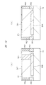
<半導体素子の断面デバイス構造>
続いて、本実施の形態における半導体素子の断面デバイス構造について説明する。図4は、図3のA−A線で切断した断面図である。図4に示すように、本実施の形態における半導体素子SD1は、p型の半導体基板1Sを有し、この半導体基板1S上に、n型半導体層からなるエピタキシャル層EPIが形成されている。
<Cross-section device structure of semiconductor element>
Subsequently, the cross-sectional device structure of the semiconductor element in the present embodiment will be described. FIG. 4 is a sectional view taken along line AA of FIG. As shown in FIG. 4, the semiconductor element SD1 in the present embodiment has a p-
そして、半導体基板1Sとエピタキシャル層EPIの境界に跨って、エピタキシャル層EPIよりも不純物濃度の高いn型半導体領域である埋込半導体領域BSRが形成されている。さらに、図4に示すように、埋込半導体領域BSRと離間しながら、半導体基板1Sと接触するp型半導体領域からなる分離半導体領域ISOが形成されている。この分離半導体領域ISOは、例えば、半導体基板1Sと接触するp型半導体領域PR1と、このp型半導体領域PR1上に形成されたp型半導体領域PR2と、p型半導体領域PR2よりも不純物濃度の高いp型半導体領域PR3とから構成されている。
Then, a buried semiconductor region BSR, which is an n-type semiconductor region having an impurity concentration higher than that of the epitaxial layer EPI, is formed across the boundary between the
このように構成されている分離半導体領域ISOは、図4では示されていないが、図2に示すグランド端子GNDと電気的に接続されている。したがって、分離半導体領域ISOと接触している半導体基板1Sもグランド端子GNDと電気的に接続されていることになる。このことから、半導体基板1Sを分離半導体領域ISOと電気的に接続することにより、半導体基板1Sに安定したグランド電位を供給することが可能となる。すなわち、分離半導体領域ISOは、エピタキシャル層EPIに形成される他の半導体素子から半導体素子SD1を電気的に分離する機能を有するとともに、半導体基板1Sに安定したグランド電位を供給する機能を有していることになる。
Although not shown in FIG. 4, the isolation semiconductor region ISO thus configured is electrically connected to the ground terminal GND shown in FIG. Therefore, the
次に、図4に示すように、エピタキシャル層EPIの表面には、例えば、選択酸化法により形成された酸化シリコン膜からなる分離絶縁膜(LOCOS)LSが形成されており、分離絶縁膜LSで挟まれたエピタキシャル層EPIの表面に抵抗素子として機能する抵抗領域RRが形成されている。この抵抗領域RRは、例えば、p型半導体領域から構成されている。そして、図4に示すように、埋込半導体領域BSRと接触し、かつ、エピタキシャル層EPIの表面にまで達し、かつ、エピタキシャル層EPIよりも不純物濃度の高いn型半導体領域からなるシンカー領域SKRが形成されている。このシンカー領域SKRは、例えば、埋込半導体領域BSRと接触するn型半導体領域NR1と、n型半導体領域NR1よりも不純物濃度の高いn型半導体領域NR2とから構成されている。 Next, as shown in FIG. 4, an isolation insulating film (LOCOS) LS made of, for example, a silicon oxide film formed by a selective oxidation method is formed on the surface of the epitaxial layer EPI. A resistance region RR that functions as a resistance element is formed on the surface of the sandwiched epitaxial layer EPI. The resistance region RR is composed of, for example, a p-type semiconductor region. Then, as shown in FIG. 4, a sinker region SKR which is in contact with the buried semiconductor region BSR and reaches the surface of the epitaxial layer EPI and which is composed of an n-type semiconductor region having a higher impurity concentration than the epitaxial layer EPI is formed. Has been formed. The sinker region SKR is composed of, for example, an n-type semiconductor region NR1 which is in contact with the buried semiconductor region BSR and an n-type semiconductor region NR2 having an impurity concentration higher than that of the n-type semiconductor region NR1.
続いて、図4に示すように、分離絶縁膜LS上には、部分的に窒化シリコン膜SNFが形成されており、この窒化シリコン膜SNF上にポリシリコン膜PFが形成されている。特に、シンカー領域SKRと平面的に重なる位置においては、分離絶縁膜LSと窒化シリコン膜SNFを貫通する開口部OPが形成されおり、この開口部OPには、ポリシリコン膜PFが埋め込まれている。すなわち、開口部OPからは、シンカー領域SKRが露出しており、この露出するシンカー領域SKRと接触するように、開口部OP内にポリシリコン膜PFが形成されている。 Subsequently, as shown in FIG. 4, a silicon nitride film SNF is partially formed on the isolation insulating film LS, and a polysilicon film PF is formed on the silicon nitride film SNF. In particular, an opening OP penetrating the isolation insulating film LS and the silicon nitride film SNF is formed at a position that overlaps the sinker region SKR in plan view, and the polysilicon film PF is embedded in the opening OP. .. That is, the sinker region SKR is exposed from the opening OP, and the polysilicon film PF is formed in the opening OP so as to be in contact with the exposed sinker region SKR.
そして、図4に示すように、ポリシリコン膜PFの表面および分離絶縁膜LSの表面を覆うように、エピタキシャル層EPIの上方に、例えば、酸化シリコン膜からなる層間絶縁膜ILが形成されている。そして、この層間絶縁膜ILには、層間絶縁膜ILを貫通して、ポリシリコン膜PFに達するプラグPLG3が形成されている。さらに、層間絶縁膜IL上には、プラグPLG3と電気的に接続される配線WL1が形成されている。したがって、図4に示すように、埋込半導体領域BSRとシンカー領域SKRとポリシリコン膜PFとプラグPLG3と配線WL1とは、電気的に接続されていることになる。 Then, as shown in FIG. 4, an interlayer insulating film IL made of, for example, a silicon oxide film is formed above the epitaxial layer EPI so as to cover the surface of the polysilicon film PF and the surface of the isolation insulating film LS. .. Then, in the interlayer insulating film IL, a plug PLG3 penetrating the interlayer insulating film IL and reaching the polysilicon film PF is formed. Further, the wiring WL1 electrically connected to the plug PLG3 is formed on the interlayer insulating film IL. Therefore, as shown in FIG. 4, the buried semiconductor region BSR, the sinker region SKR, the polysilicon film PF, the plug PLG3, and the wiring WL1 are electrically connected.
次に、図5は、図3のB−B線で切断した断面図である。図5に示すように、本実施の形態における半導体素子SD1は、半導体基板1Sと半導体基板1S上に形成されたエピタキシャル層EPIとを有する。そして、エピタキシャル層EPIには、分離半導体領域ISOが形成されており、この分離半導体領域ISOで挟まれる位置に、埋込半導体領域BSRが形成されている。そして、エピタキシャル層EPIの表面には、分離絶縁膜LSが形成されており、分離絶縁膜LSで挟まれるエピタキシャル層EPIの表面に抵抗領域RRが形成されている。さらに、エピタキシャル層EPIの上方には、層間絶縁膜ILが形成されており、この層間絶縁膜ILには、層間絶縁膜ILを貫通して、抵抗領域RRに達するプラグPLG1およびプラグPLG2が形成されている。すなわち、抵抗領域RRの一端部ED1と電気的に接続するプラグPLG1と、抵抗領域RRの他端部ED2と電気的に接続するプラグPLG2とが、層間絶縁膜ILに形成されている。そして、層間絶縁膜IL上には、プラグPLG1と電気的に接続される配線WL1と、プラグPLG2と電気的に接続される配線WL2とが形成されている。
Next, FIG. 5 is a cross-sectional view taken along line BB of FIG. As shown in FIG. 5, the semiconductor element SD1 in the present embodiment has a
以上のことから、例えば、図4に示すように、埋込半導体領域BSRとシンカー領域SKRとポリシリコン膜PFとプラグPLG3と配線WL1とは、電気的に接続されており、かつ、例えば、図5に示すように、抵抗領域RRの一端部ED1と配線WL1とは、電気的に接続されていることになる。したがって、抵抗領域RRの一端部ED1と埋込半導体領域BSRとシンカー領域SKRとポリシリコン膜PFとプラグPLG3と配線WL1とは、電気的に接続されていることになる。 From the above, for example, as shown in FIG. 4, the buried semiconductor region BSR, the sinker region SKR, the polysilicon film PF, the plug PLG3, and the wiring WL1 are electrically connected and, for example, as shown in FIG. As shown in FIG. 5, the one end ED1 of the resistance region RR and the wiring WL1 are electrically connected. Therefore, the one end ED1 of the resistance region RR, the buried semiconductor region BSR, the sinker region SKR, the polysilicon film PF, the plug PLG3, and the wiring WL1 are electrically connected.
なお、図4および図5に示すように、断面視において、埋込半導体領域BSRの一端部(左端部)ED1と左側の分離半導体領域ISOとの間の距離(第1距離)と、埋込半導体領域BSRの他端部(右端部)ED2と右側の分離半導体領域ISOとの間の距離(第2距離)とは、互いに等しくなっている。 As shown in FIGS. 4 and 5, in a cross-sectional view, the distance (first distance) between one end (left end) ED1 of the embedded semiconductor region BSR and the left isolation semiconductor region ISO, and the embedded The distance (second distance) between the other end (right end) ED2 of the semiconductor region BSR and the right-side isolation semiconductor region ISO is equal to each other.
このように構成されている半導体素子SD1は、抵抗素子としての機能と、静電保護素子としての機能とを有する。具体的に、本実施の形態における半導体素子SD1において、抵抗素子は、抵抗領域RRから構成される一方、静電保護素子は、抵抗領域RRをエミッタとし、エピタキシャル層EPIおよび埋込半導体領域BSRをベースとし、半導体基板1Sをコレクタとする寄生バイポーラトランジスタから構成される。
The semiconductor element SD1 thus configured has a function as a resistance element and a function as an electrostatic protection element. Specifically, in the semiconductor element SD1 in the present embodiment, the resistance element is formed of the resistance region RR, while the electrostatic protection element has the resistance region RR as the emitter and the epitaxial layer EPI and the buried semiconductor region BSR as the emitter. It is composed of a parasitic bipolar transistor having a base and a
つまり、例えば、図4に示すように、本実施の形態における半導体素子SD1は、半導体基板1Sと、半導体基板1S上に形成されたエピタキシャル層EPIと、エピタキシャル層EPI内に形成された抵抗領域RR(抵抗素子)と、抵抗領域RRを構成要素とするバイポーラトランジスタからなる静電保護素子とを備える。
That is, for example, as shown in FIG. 4, the semiconductor element SD1 in the present embodiment includes a
このとき、本実施の形態における半導体素子SD1は、エピタキシャル層EPI内に形成され、かつ、エピタキシャル層EPIよりも不純物濃度が高く、かつ、抵抗領域RRと電気的に接続され、かつ、抵抗領域RRとは逆導電型の埋込半導体領域BSRを有する。 At this time, the semiconductor element SD1 in the present embodiment is formed in the epitaxial layer EPI, has a higher impurity concentration than the epitaxial layer EPI, is electrically connected to the resistance region RR, and is also in the resistance region RR. And a buried semiconductor region BSR of opposite conductivity type.
そして、静電保護素子となるバイポーラトランジスタは、エミッタとして機能する抵抗領域RRと、ベースとして機能する埋込半導体領域と、コレクタとして機能する半導体基板1Sとから構成されている。
The bipolar transistor that serves as an electrostatic protection element includes a resistance region RR that functions as an emitter, a buried semiconductor region that functions as a base, and a
ここで、本実施の形態における半導体素子SD1は、例えば、図4に示すように、平面視において埋込半導体領域BSRを囲み、かつ、半導体基板1Sと電気的に接続され、かつ、半導体基板1Sと同じ導電型である分離半導体領域ISOを有する。
Here, the semiconductor element SD1 in the present embodiment, for example, as shown in FIG. 4, surrounds the embedded semiconductor region BSR in a plan view, is electrically connected to the
<具体的な設計数値例>
次に、具体的な設計数値例について説明する。図4において、抵抗領域RRは、p型半導体領域から構成され、例えば、抵抗領域RRの不純物濃度は、約1×10¹⁹(atoms/cm3)となっているが、これに限らず、1×1017(atoms/cm3)〜1×1021(atoms/cm3)の範囲であってもよい。
<Specific design numerical example>
Next, a specific design numerical example will be described. In FIG. 4, the resistance region RR is composed of a p-type semiconductor region, and for example, the impurity concentration of the resistance region RR is about 1×10 19 (atoms/cm 3 ). It may be in the range of ×10 17 (atoms/cm 3 ) to 1×10 21 (atoms/cm 3 ).
エピタキシャル層EPIは、n型半導体層から構成されている。このエピタキシャル層EPIの厚さは、例えば、10μmであり、エピタキシャル層EPIの不純物濃度は、例えば、約1×10¹⁵(atoms/cm3)である。ただし、これに限らず、エピタキシャル層EPIの厚さは、5μm〜18μmであってもよく、エピタキシャル層EPIの不純物濃度は、1×1014(atoms/cm3)〜1×1017(atoms/cm3)の範囲であってもよい。 The epitaxial layer EPI is composed of an n-type semiconductor layer. The thickness of the epitaxial layer EPI is, for example, 10 μm, and the impurity concentration of the epitaxial layer EPI is, for example, about 1×10 15 (atoms/cm 3 ). However, not limited to this, the thickness of the epitaxial layer EPI may be 5 μm to 18 μm, and the impurity concentration of the epitaxial layer EPI is 1×10 14 (atoms/cm 3 ) to 1×10 17 (atoms/ It may be in the range of cm 3 ).
シンカー領域SKRは、n型半導体領域NR1とn型半導体領域NR2とから構成され、n型半導体領域NR1の不純物濃度は、例えば、5×10¹⁶(atoms/cm3)であり、n型半導体領域NR2の不純物濃度は、例えば、1×1020(atoms/cm3)である。ただし、これに限らず、n型半導体領域NR1の不純物濃度は、例えば、5×1015(atoms/cm3)であってもよく、n型半導体領域NR2の不純物濃度は、例えば、1×1021(atoms/cm3)であってもよい。なお、シンカー領域SKRの不純物濃度は、エピタキシャル層EPIの不純物濃度の10倍以上であることが望ましい。 The sinker region SKR is composed of an n-type semiconductor region NR1 and an n-type semiconductor region NR2, the impurity concentration of the n-type semiconductor region NR1 is, for example, 5×10 16 (atoms/cm 3 ), and the n-type semiconductor region is The impurity concentration of NR2 is, for example, 1×10 20 (atoms/cm 3 ). However, the impurity concentration of the n-type semiconductor region NR1 may be, for example, 5×10 15 (atoms/cm 3 ) and the impurity concentration of the n-type semiconductor region NR2 may be, for example, 1×10 5. It may be 21 (atoms/cm 3 ). The impurity concentration of the sinker region SKR is preferably 10 times or more the impurity concentration of the epitaxial layer EPI.
埋込半導体領域BSRは、n型半導体領域から構成され、例えば、埋込半導体領域BSRの不純物濃度は、約2×10¹⁸(atoms/cm3)であるが、これに限らず、埋込半導体領域BSRの不純物濃度は、約1×1020(atoms/cm3)であってもよい。 The buried semiconductor region BSR is composed of an n-type semiconductor region. For example, the buried semiconductor region BSR has an impurity concentration of about 2×10 18 (atoms/cm 3 ), but the buried semiconductor region BSR is not limited to this. The impurity concentration of the region BSR may be about 1×10 20 (atoms/cm 3 ).
分離半導体領域ISOは、p型半導体領域PR1とp型半導体領域PR2とp型半導体領域PR3とから構成されている。p型半導体領域PR1の不純物濃度は、例えば、約5×10¹⁷(atoms/cm3)であるが、これに限らず、p型半導体領域PR1の不純物濃度は、約1×1020(atoms/cm3)であってもよい。また、p型半導体領域PR2の不純物濃度およびp型半導体領域PR3の不純物濃度は、例えば、約1×1019(atoms/cm3)であるが、これに限らず、p型半導体領域PR2の不純物濃度およびp型半導体領域PR3の不純物濃度は、約1×1020(atoms/cm3)であってもよい。この分離半導体領域ISOは、抵抗領域RRからなる抵抗素子を他の半導体素子と分離する機能と、半導体基板1Sの電位を固定する機能とを有している。図4では、図示していないが、分離半導体領域ISOは、プラグを介して配線と電気的に接続されており、最終的に、図2に示すグランド端子GNDと電気的に接続されている。
The isolation semiconductor region ISO is composed of a p-type semiconductor region PR1, a p-type semiconductor region PR2 and a p-type semiconductor region PR3. The impurity concentration of the p-type semiconductor region PR1 is, for example, about 5×10 17 (atoms/cm 3 ), but not limited to this, the impurity concentration of the p-type semiconductor region PR1 is about 1×10 20 (atoms/cm 3 ). cm 3 ). The impurity concentration of the p-type semiconductor region PR2 and the impurity concentration of the p-type semiconductor region PR3 are, for example, about 1×10 19 (atoms/cm 3 ), but the impurity concentration of the p-type semiconductor region PR2 is not limited to this. The concentration and the impurity concentration of the p-type semiconductor region PR3 may be about 1×10 20 (atoms/cm 3 ). The isolation semiconductor region ISO has a function of isolating the resistance element including the resistance region RR from other semiconductor elements and a function of fixing the potential of the
図4において、シンカー領域SKRは、ポリシリコン膜PFおよびプラグPLG3を介して配線WL1と接続されている。一方、図5において、抵抗領域RRの一端部(左端部)ED1は、プラグPLG1を介して配線WL1と電気的に接続され、かつ、抵抗領域RRの他端部(右端部)ED2は、プラグPLG2を介して配線WL2と電気的に接続されている。そして、配線WL1は、図2に示す入力端子INと電気的に接続される一方、配線WL2は、図2に示す入力トランジスタTrのベースと電気的に接続されている。 In FIG. 4, the sinker region SKR is connected to the wiring WL1 via the polysilicon film PF and the plug PLG3. On the other hand, in FIG. 5, one end (left end) ED1 of the resistance region RR is electrically connected to the wiring WL1 via the plug PLG1, and the other end (right end) ED2 of the resistance region RR is a plug. It is electrically connected to the wiring WL2 via the PLG2. The wiring WL1 is electrically connected to the input terminal IN shown in FIG. 2, while the wiring WL2 is electrically connected to the base of the input transistor Tr shown in FIG.
ここで、プラグPLG1〜PLG3は、例えば、タングステンプラグから構成されるが、これに限らず、アルミニウムプラグから構成してもよい。また、配線WL1および配線WL2は、例えば、アルミニウム配線から構成されている。 Here, although the plugs PLG1 to PLG3 are made of, for example, tungsten plugs, the plugs PLG1 to PLG3 may be made of aluminum plugs without being limited to this. The wiring WL1 and the wiring WL2 are made of, for example, aluminum wiring.
図4および図5において、埋込半導体領域BSRとp型半導体領域PR1との間の距離は、約1μmとなっている。この埋込半導体領域BSRとp型半導体領域PR1との間の逆接合耐圧が一番低くなっており、埋込半導体領域BSRとp型半導体領域PR1との間に50Vの電位差が生じると、埋込半導体領域BSRとp型半導体領域PR1との間にリーク電流が流れ始める。なお、埋込半導体領域BSRとp型半導体領域PR1との間の距離は、0μm〜20μmの範囲でもよい。ただし、図2に示す入力端子INにプラスのサージ電荷が入ったときに、埋込半導体領域BSRとp型半導体領域PR1との間で初めに降伏するような距離に設計することが望ましく、その逆接合耐圧は、製品仕様の最大電圧以上で、図2に示す入力トランジスタTIrの破壊電圧未満である必要がある。 4 and 5, the distance between the buried semiconductor region BSR and the p-type semiconductor region PR1 is about 1 μm. The reverse junction withstand voltage between the buried semiconductor region BSR and the p-type semiconductor region PR1 is the lowest, and when a potential difference of 50 V occurs between the buried semiconductor region BSR and the p-type semiconductor region PR1, the buried junction region BSR and the p-type semiconductor region PR1 are buried. A leak current begins to flow between the embedded semiconductor region BSR and the p-type semiconductor region PR1. The distance between the buried semiconductor region BSR and the p-type semiconductor region PR1 may be in the range of 0 μm to 20 μm. However, it is desirable to design the distance so that the buried semiconductor region BSR and the p-type semiconductor region PR1 will first break down when a positive surge charge enters the input terminal IN shown in FIG. The reverse junction withstand voltage must be equal to or higher than the maximum voltage of the product specifications and lower than the breakdown voltage of the input transistor TIr shown in FIG.
<半導体素子の動作>
本実施の形態における半導体素子SD1は、上記のように構成されており、以下に、静電保護素子となる寄生バイポーラトランジスタの動作について説明する。特に、図2に示す入力端子INにプラスのサージ電荷が入った場合における半導体素子SD1の動作について説明することにする。この動作の説明は、段階的にサージ電荷を増加していった場合において、図4に対応する模式図とI−Vカーブを使用して行なわれる。
<Operation of semiconductor device>
The semiconductor element SD1 in the present embodiment is configured as described above, and the operation of the parasitic bipolar transistor serving as an electrostatic protection element will be described below. In particular, the operation of the semiconductor element SD1 when a positive surge charge enters the input terminal IN shown in FIG. 2 will be described. This operation will be described using the schematic diagram corresponding to FIG. 4 and the IV curve when the surge charge is increased stepwise.
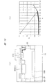
図6(a)は、図4に対応する模式図であり、図6(b)は、I−Vカーブを示すグラフである。図6(b)において、I−Vカーブの横軸は、サージ電荷が図2に示す入力端子INに入った場合に、図3および図5に示す抵抗領域RRの一端部ED1に印加される電圧を示している。一方、I−Vカーブの縦軸は、抵抗領域RRの一端部ED1に流れる電流を示している。この電流が大きいほど、多くのサージ電荷を図2に示すグランド端子GNDに受け流すことができることを示しており、静電破壊耐量が高いことになる。 FIG. 6A is a schematic diagram corresponding to FIG. 4, and FIG. 6B is a graph showing an IV curve. In FIG. 6B, the horizontal axis of the IV curve is applied to the one end portion ED1 of the resistance region RR shown in FIGS. 3 and 5 when the surge charge enters the input terminal IN shown in FIG. It shows the voltage. On the other hand, the vertical axis of the IV curve shows the current flowing through the one end ED1 of the resistance region RR. It is shown that the larger this current is, the more surge charges can be received and supplied to the ground terminal GND shown in FIG. 2, and the higher the electrostatic breakdown withstand capability is.
まず、図6(a)は、図2に示す入力端子INに入ったサージ電荷により、抵抗領域RRの一端部ED1に40Vの電位が印加された場合の説明図である。図6(a)に示すように、図2に示すグランド端子GNDと電気的に接続されている分離半導体領域ISOと半導体基板1Sには、0Vの基準電位が印加されている。一方、図2に示す入力端子INと電気的に接続されている抵抗領域RRとシンカー領域SKRと埋込半導体領域BSRとエピタキシャル層EPIには、40Vの電位が印加されている。この状態は、図6(b)に示すI−Vカーブのポイント(1)に対応しており、抵抗領域RRの一端部ED1には電流は流れていない。つまり、40Vの電位は、製品仕様上、通常動作で印加される範囲内の電位であり、図2に示す入力端子INに入ったサージ電荷による静電破壊は生じないレベルである。このことから、サージ電荷をグランド端子GNDに受け流すために抵抗領域RRの一端部ED1からグランド端子GNDへ流れる電流は発生していない。
First, FIG. 6A is an explanatory diagram in the case where a potential of 40 V is applied to the one end portion ED1 of the resistance region RR by the surge charge that has entered the input terminal IN shown in FIG. As shown in FIG. 6A, a reference potential of 0 V is applied to the isolation semiconductor region ISO and the
次に、図7(a)は、図4に対応する模式図であり、図7(b)は、I−Vカーブを示すグラフである。特に、図7(a)は、図2に示す入力端子INに入ったサージ電荷により、抵抗領域RRの一端部ED1に50Vの電位が印加された場合の説明図である。図7(a)に示すように、抵抗領域RRの一端部ED1は、50Vの電位に固定されている。一方、本実施の形態における半導体素子SD1では、埋込半導体領域BSRと分離半導体領域ISOとの間に50Vの逆バイアスが印加される結果、埋込半導体領域BSRと分離半導体領域ISOとの間にリーク電流が流れ始める。したがって、図7(a)に示すように、エピタキシャル層EPIとシンカー領域SKRと埋込半導体領域BSRでは、リーク電流が流れるために。オームの法則に従った電位ドロップが発生する。これにより、例えば、図7(a)に示すように、エピタキシャル層EPIの電位は、約49.7Vとなり、埋込半導体領域BSRの電位は、49.5Vとなる。このように、図7(a)に示す状態では、抵抗領域RRの一端部ED1は、50Vの電位に固定されているが、抵抗領域RRに接するエピタキシャル層EPIの電位は、抵抗領域RRの一端部ED1よりも低い電位となる。この結果、抵抗領域RRの一端部ED1とエピタキシャル層EPIとの間のpn接合には順バイアスが印加されることになるが、この順バイアス(0.3V)は、pn接合のビルトインポテンシャル(0.7V)よりも小さいため、抵抗領域RRの一端部ED1からエピタキシャル層EPIへの電流は流れない。この図7(a)に示す状態は、図7(b)に示すI−Vカーブのポイント(2)に対応している。 Next, FIG. 7A is a schematic diagram corresponding to FIG. 4, and FIG. 7B is a graph showing an IV curve. In particular, FIG. 7A is an explanatory diagram in the case where a potential of 50 V is applied to the one end portion ED1 of the resistance region RR by the surge charge that has entered the input terminal IN shown in FIG. As shown in FIG. 7A, one end portion ED1 of the resistance region RR is fixed at a potential of 50V. On the other hand, in the semiconductor element SD1 in the present embodiment, a reverse bias of 50 V is applied between the embedded semiconductor region BSR and the isolation semiconductor region ISO, and as a result, the embedded semiconductor region BSR and the isolation semiconductor region ISO are applied. Leak current begins to flow. Therefore, as shown in FIG. 7A, a leak current flows in the epitaxial layer EPI, the sinker region SKR, and the buried semiconductor region BSR. A potential drop occurs according to Ohm's law. As a result, for example, as shown in FIG. 7A, the potential of the epitaxial layer EPI becomes about 49.7V and the potential of the buried semiconductor region BSR becomes 49.5V. Thus, in the state shown in FIG. 7A, the one end ED1 of the resistance region RR is fixed to the potential of 50 V, but the potential of the epitaxial layer EPI in contact with the resistance region RR is one end of the resistance region RR. The potential becomes lower than that of the portion ED1. As a result, a forward bias is applied to the pn junction between the one end portion ED1 of the resistance region RR and the epitaxial layer EPI. This forward bias (0.3 V) is the built-in potential (0 V of the pn junction. 0.7 V), no current flows from the one end ED1 of the resistance region RR to the epitaxial layer EPI. The state shown in FIG. 7A corresponds to the point (2) of the IV curve shown in FIG. 7B.
続いて、図8(a)は、図4に対応する模式図であり、図8(b)は、I−Vカーブを示すグラフである。特に、図8(a)は、図2に示す入力端子INに入ったサージ電荷により、抵抗領域RRの一端部ED1に110Vの電位が印加された場合の説明図である。図8(a)に示すように、抵抗領域RRの一端部ED1は、110Vの電位に固定されている。一方、本実施の形態における半導体素子SD1では、埋込半導体領域BSRと分離半導体領域ISOとの間に110Vの逆バイアスが印加される結果、埋込半導体領域BSRと分離半導体領域ISOとの間に流れるリーク電流が増加する。この結果、図8(a)に示すように、エピタキシャル層EPIとシンカー領域SKRと埋込半導体領域BSRでは、リーク電流が増加するためにオームの法則に従った電位ドロップが大きくなる。これにより、例えば、図8(a)に示すように、エピタキシャル層EPIの電位は、約109.3Vとなり、埋込半導体領域BSRの電位は、109Vとなる。このように、図8(a)に示す状態では、抵抗領域RRの一端部ED1は、110Vの電位に固定されているが、抵抗領域RRに接するエピタキシャル層EPIの電位は、抵抗領域RRの一端部ED1よりもかなり低い電位となる。この結果、抵抗領域RRの一端部ED1とエピタキシャル層EPIとの間のpn接合には順バイアスが印加されることになり、この順バイアス(0.7V)は、pn接合のビルトインポテンシャル(0.7V)に達することになり、抵抗領域RRの一端部ED1からエピタキシャル層EPIへ電流が流れ始める。つまり、図8(a)に示す状態では、抵抗領域RRをエミッタとし、かつ、エピタキシャル層EPIをベースとし、半導体基板1Sをコレクタとする寄生バイポーラトランジスタ(PNPバイポーラトランジスタ)において、エミッタからベースに向かって電流が流れ始める。この図8(a)に示す状態は、図8(b)に示すI−Vカーブのポイント(3)に対応しており、寄生バイポーラトランジスタが動作し始める直前のポイントに対応する。
Subsequently, FIG. 8A is a schematic diagram corresponding to FIG. 4, and FIG. 8B is a graph showing an IV curve. In particular, FIG. 8A is an explanatory diagram in the case where a potential of 110 V is applied to the one end portion ED1 of the resistance region RR by the surge charge that has entered the input terminal IN shown in FIG. As shown in FIG. 8A, one end portion ED1 of the resistance region RR is fixed at a potential of 110V. On the other hand, in semiconductor device SD1 in the present embodiment, a reverse bias of 110 V is applied between embedded semiconductor region BSR and isolation semiconductor region ISO, and as a result, embedded semiconductor region BSR and isolation semiconductor region ISO are applied. The leak current that flows increases. As a result, as shown in FIG. 8 (a), the epitaxial layer EPI and sinker region SKR embedded semiconductor region BSR, the potential drops in accordance with the law of O over arm for leakage current increases increases. As a result, for example, as shown in FIG. 8A, the potential of the epitaxial layer EPI becomes about 109.3V and the potential of the embedded semiconductor region BSR becomes 109V. Thus, in the state shown in FIG. 8A, the one end ED1 of the resistance region RR is fixed to the potential of 110 V, but the potential of the epitaxial layer EPI in contact with the resistance region RR is one end of the resistance region RR. The potential is considerably lower than that of the portion ED1. As a result, a forward bias is applied to the pn junction between the one end portion ED1 of the resistance region RR and the epitaxial layer EPI, and this forward bias (0.7 V) is the built-in potential (0. 7V), and a current starts to flow from the one end ED1 of the resistance region RR to the epitaxial layer EPI. That is, in the state shown in FIG. 8A, in the parasitic bipolar transistor (PNP bipolar transistor) having the resistance region RR as the emitter, the epitaxial layer EPI as the base, and the
その後、図9(a)は、図4に対応する模式図であり、図9(b)は、I−Vカーブを示すグラフである。特に、図9(a)は、図2に示す入力端子INに入ったサージ電荷により、抵抗領域RRの一端部ED1に110Vの電位が印加された場合において、寄生バイポーラトランジスタがオン動作する状態を示す説明図である。図9(a)に示すように、抵抗領域RRをエミッタとし、かつ、エピタキシャル層EPIをベースとし、半導体基板1Sをコレクタとする寄生バイポーラトランジスタ(PNPバイポーラトランジスタ)において、エミッタからベースに向かって電流が流れる結果、寄生バイポーラトランジスタがオン動作する。これにより、抵抗領域RRの一端部ED1から、エピタキシャル層EPIおよび埋込半導体領域BSRを介して、半導体基板1Sに大電流が流れる。この図9(a)に示す状態は、図9(b)に示すI−Vカーブの範囲(4)に対応する。図9(b)に示すように、寄生バイポーラトランジスタがオン動作することにより、抵抗領域RRの一端部ED1(エミッタ)から半導体基板1S(コレクタ)に向かって大電流が流れる。この結果、図2に示す入力端子INに入ったサージ電荷がグランド端子GNDに受け流されるため、抵抗領域RRの一端部ED1に印加される電位は低下することになる。そして、図9(b)に示すポイント(5)は、大電流によって、本実施の形態における半導体素子SD1が熱破壊した結果、これ以上の電流を流すことができなくなったポイントを示しており、この電流値が本実施の形態における半導体素子SD1の静電破壊耐量を示している。
After that, FIG. 9A is a schematic diagram corresponding to FIG. 4, and FIG. 9B is a graph showing an IV curve. In particular, FIG. 9A shows a state in which the parasitic bipolar transistor is turned on when a potential of 110 V is applied to the one end ED1 of the resistance region RR due to the surge charge that has entered the input terminal IN shown in FIG. FIG. As shown in FIG. 9A, in a parasitic bipolar transistor (PNP bipolar transistor) having the resistance region RR as an emitter, the epitaxial layer EPI as a base, and the
以上のようにして、本実施の形態における半導体素子SD1によれば、図2に示す入力端子INに入ったサージ電荷が所定の電荷量に達すると、寄生バイポーラトランジスタがオン動作することにより、サージ電荷をグランド端子GNDに流すことができる。すなわち、本実施の形態における半導体素子SD1によれば、半導体素子SD1に設けられている寄生バイポーラトランジスタがオン動作することによって、サージ電荷に起因する入力端子INの電位の上昇が、入力端子INに接続されている入力トランジスタTrの破壊電圧に達する前に抑制される結果、サージ電荷に起因する入力トランジスタTrの破壊を効果的に抑制することができる。 As described above, according to the semiconductor device SD1 in the present embodiment, when the surge charge that has entered the input terminal IN shown in FIG. 2 reaches a predetermined charge amount, the parasitic bipolar transistor is turned on to cause the surge. The electric charge can flow to the ground terminal GND. That is, according to the semiconductor device SD1 in the present embodiment, the parasitic bipolar transistor provided in the semiconductor device SD1 is turned on, so that the potential increase of the input terminal IN due to the surge charge is caused to the input terminal IN. As a result of being suppressed before reaching the breakdown voltage of the connected input transistor Tr, breakdown of the input transistor Tr due to surge charge can be effectively suppressed.
<実施の形態における特徴>
次に、本実施の形態における特徴点について説明する。本実施の形態における第1特徴点は、専用の静電保護素子を設けるのではなく、別の機能を有する他の半導体素子に静電保護素子の機能を付加する点にある。すなわち、本実施の形態では、別の機能を有する半導体素子に静電保護素子としての機能も追加する。これにより、本実施の形態における第1特徴点によれば、専用の静電保護素子を設ける必要がなくなるため、半導体装置の静電破壊耐量を向上しながらも、半導体装置の小型化を実現することができる。
<Characteristics of the embodiment>
Next, the features of the present embodiment will be described. The first feature of the present embodiment is that a dedicated electrostatic protection element is not provided, but the function of the electrostatic protection element is added to another semiconductor element having another function. That is, in this embodiment, a function as an electrostatic protection element is added to a semiconductor element having another function. As a result, according to the first feature of the present embodiment, it is not necessary to provide a dedicated electrostatic protection element, so that the semiconductor device can be downsized while improving the electrostatic breakdown withstand capability of the semiconductor device. be able to.
特に、本実施の形態では、例えば、図2に示すように、静電保護機能とは別の機能を有する抵抗素子Rに、静電保護機能を有する寄生バイポーラトランジスタQを付加したデバイス構造を有する半導体素子SD1を形成している。具体的に、本実施の形態では、図4に示すように、抵抗素子として機能する抵抗領域RRを有するデバイス構造に、静電保護素子として機能する寄生バイポーラトランジスタのデバイス構造を付加している。つまり、図4に示す半導体素子SD1のデバイス構造において、抵抗領域RRをエミッタとし、エピタキシャル層EPIおよび埋込半導体領域BSRをベースとし、半導体基板1SをコレクタとするPNPバイポーラトランジスタによって、寄生バイポーラトランジスタが形成されている。そして、本実施の形態では、この寄生バイポーラトランジスタが静電保護素子として機能するように、寄生バイポーラトランジスタのデバイス構造に工夫を施しており、この工夫点が本実施の形態における第2特徴点である。
In particular, this embodiment has a device structure in which a parasitic bipolar transistor Q having an electrostatic protection function is added to a resistance element R having a function different from the electrostatic protection function, as shown in FIG. The semiconductor element SD1 is formed. Specifically, in the present embodiment, as shown in FIG. 4, a device structure of a parasitic bipolar transistor functioning as an electrostatic protection element is added to a device structure having a resistance region RR functioning as a resistance element. That is, in the device structure of the semiconductor element SD1 shown in FIG. 4, the parasitic region becomes a parasitic bipolar transistor by the PNP bipolar transistor having the resistance region RR as the emitter, the epitaxial layer EPI and the buried semiconductor region BSR as the base, and the
すなわち、本実施の形態における第2特徴点は、例えば、図4に示すように、埋込半導体領域BSRと接触し、かつ、エピタキシャル層EPIの表面にまで達し、かつ、エピタキシャル層EPIよりも不純物濃度の高いn型半導体領域からなるシンカー領域SKRを形成している点にある。つまり、本実施の形態における第2特徴点は、エピタキシャル層EPI内に、n型半導体領域NR2を含むシンカー領域SKRを形成している点にある。 That is, the second characteristic point in the present embodiment is, for example, as shown in FIG. 4, in contact with the buried semiconductor region BSR, reaching the surface of the epitaxial layer EPI, and being more impurity than the epitaxial layer EPI. The point is that the sinker region SKR formed of the n-type semiconductor region with high concentration is formed. That is, the second characteristic point of the present embodiment is that the sinker region SKR including the n-type semiconductor region NR2 is formed in the epitaxial layer EPI.
これにより、上述した<半導体素子の動作>の欄で説明したように、本実施の形態における半導体素子SD1によれば、図2に示す入力端子INに入ったサージ電荷が所定の電荷量に達した場合に、寄生バイポーラトランジスタをオン動作させることによって、サージ電荷をグランド端子GNDに流すことができる。すなわち、本実施の形態における半導体素子SD1によれば、半導体素子SD1に設けられている寄生バイポーラトランジスタがオン動作することによって、サージ電荷に起因する入力端子INの電位の上昇が、入力端子INに接続されている入力トランジスタTrの破壊電圧に達する前に抑制される結果、サージ電荷に起因する入力トランジスタTrの破壊を効果的に抑制することができる。 As a result, as described above in the section <Operation of semiconductor device>, according to the semiconductor device SD1 of the present embodiment, the surge charge that has entered the input terminal IN shown in FIG. 2 reaches a predetermined charge amount. In such a case, by turning on the parasitic bipolar transistor, surge charge can flow to the ground terminal GND. That is, according to the semiconductor device SD1 in the present embodiment, the parasitic bipolar transistor provided in the semiconductor device SD1 is turned on, so that the potential increase of the input terminal IN due to the surge charge is caused to the input terminal IN. As a result of being suppressed before reaching the breakdown voltage of the connected input transistor Tr, breakdown of the input transistor Tr due to surge charge can be effectively suppressed.
特に、本実施の形態では、リーク電流経路(図7(a)におけるシンカー領域SKR→埋込半導体領域BSR→分離半導体領域ISOの電流経路)に、n型半導体領域NR2を含むシンカー領域SKRを設けている(第2特徴点)。このため、本実施の形態によれば、シンカー領域SKRを設けないデバイス構造に比べて、寄生バイポーラトランジスタを安定的に動作させることができる。以下に、この点について説明する。 In particular, in the present embodiment, the sinker region SKR including the n-type semiconductor region NR2 is provided in the leak current route (current path of sinker region SKR→embedded semiconductor region BSR→isolation semiconductor region ISO in FIG. 7A) . (Second feature point). Therefore, according to the present embodiment, the parasitic bipolar transistor can be operated more stably than in the device structure in which the sinker region SKR is not provided. This point will be described below.
図10は、n型半導体領域NR2を含むシンカー領域SKRが形成されていない検討技術を示す図である。特に、図10(a)は、検討技術におけるデバイス構造を示す模式図であり、図10(b)は、検討技術におけるI−Vカーブを示すグラフである。 FIG. 10 is a diagram showing a study technique in which the sinker region SKR including the n-type semiconductor region NR2 is not formed. In particular, FIG. 10A is a schematic diagram showing a device structure in the study technique, and FIG. 10B is a graph showing an IV curve in the study technique.
まず、図10(a)に示す検討技術おいて、シンカー領域SKRが形成されていない場合を考える。この場合、サージ電荷によって、突発的な電位変動が生じると、pn接合に逆バイアスが加わることになり、この逆バイアスに起因するpn接合の降伏は、図10(a)に示す埋込半導体領域BSRと分離半導体領域ISOとの間の局所的な深い領域で生じる。ただし、検討技術では、降伏が生じた後、降伏によるリーク電流が増加するにしたがって、図10(a)の矢印の経路に示すように、n型半導体領域NR2→エピタキシャル層EPIの表面→分離半導体領域ISOの電流経路でリーク電流が流れるようになる。このように、エピタキシャル層EPIの表面がリーク電流の電流経路となると、小さな電流でもエピタキシャル層EPIの表面に「ミミズ」の這ったような「電流焼け跡」が形成されてしまい、この「電流焼け跡」に沿って、エピタキシャル層EPIと分離半導体領域ISOとの間にショート不良が発生する。すなわち、検討技術では、リーク電流がエピタキシャル層EPIの表面を流れる結果、エピタキシャル層EPIの表面に「電流焼け跡」が形成され、この「電流焼け跡」によって、エピタキシャル層EPIと分離半導体領域ISOとが電気的に導通してしまうのである。 First, consider the case where the sinker region SKR is not formed in the study technique shown in FIG. In this case, when a sudden potential change occurs due to the surge charge, a reverse bias is applied to the pn junction, and the breakdown of the pn junction due to this reverse bias is caused by the buried semiconductor region shown in FIG. It occurs in a locally deep region between the BSR and the isolation semiconductor region ISO. However, in the study technique, after the breakdown occurs, as the leakage current due to the breakdown increases, as shown by the path of the arrow in FIG. 10A, the n-type semiconductor region NR2→the surface of the epitaxial layer EPI→the isolation semiconductor A leak current flows in the current path of the region ISO. In this way, when the surface of the epitaxial layer EPI serves as a current path for the leak current, a “current burn trace” like “earthworm” is formed on the surface of the epitaxial layer EPI even with a small current, and this “current burn trace” is formed. A short circuit defect occurs between the epitaxial layer EPI and the isolation semiconductor region ISO along the line. That is, in the study technique, as a result of the leak current flowing on the surface of the epitaxial layer EPI, a “current burn trace” is formed on the surface of the epitaxial layer EPI, and the “current burn trace” electrically connects the epitaxial layer EPI and the isolation semiconductor region ISO. It will be electrically conducted.
これに対し、例えば、図4に示す本実施の形態における半導体素子SD1のデバイス構造では、n型半導体領域NR1を含むシンカー領域SKRが形成されている。この場合、図7(a)に示すように、サージ電荷に起因するpn接合の降伏は、埋込半導体領域BSRと分離半導体領域ISOとの間の局所的な深い領域で生じる。その後、本実施の形態では、エピタキシャル層EPIよりも不純物濃度の高いシンカー領域SKRが形成されているため、リーク電流が増加しても、リーク電流は、抵抗の高いエピタキシャル層EPIの表面を流れるのではなく、抵抗の低いシンカー領域SKRに流れ込む。すなわち、n型半導体領域NR1を含むシンカー領域SKRを形成するという本実施の形態における第2特徴点を採用すると、エピタキシャル層EPIの表面がリーク電流の電流経路とならないのである。この結果、本実施の形態における半導体素子SD1によれば、エピタキシャル層EPIの表面に「電流焼け跡」が形成されることを回避することができ、これによって、「電流焼け跡」に起因するエピタキシャル層EPIと分離半導体領域ISOとの間の導通不良を防止できることになる。したがって、本実施の形態における半導体素子SD1によれば、n型半導体領域NR1を含むシンカー領域SKRが形成されていることから、大きなリーク電流を流すことができる結果、「電流焼け跡」を形成することなく、寄生バイポーラトランジスタを動作させることができるのである。 On the other hand, for example, in the device structure of the semiconductor element SD1 in the present embodiment shown in FIG. 4, the sinker region SKR including the n-type semiconductor region NR1 is formed. In this case, as shown in FIG. 7A , the breakdown of the pn junction due to the surge charge occurs in a locally deep region between the buried semiconductor region BSR and the isolation semiconductor region ISO. After that, in the present embodiment, since the sinker region SKR having the impurity concentration higher than that of the epitaxial layer EPI is formed, even if the leak current increases, the leak current flows on the surface of the epitaxial layer EPI having high resistance. Instead, it flows into the sinker region SKR having a low resistance. That is, if the second characteristic point of the present embodiment of forming the sinker region SKR including the n-type semiconductor region NR1 is adopted, the surface of the epitaxial layer EPI does not serve as a current path for the leak current. As a result, according to the semiconductor device SD1 in the present embodiment, it is possible to avoid the formation of the “current burn mark” on the surface of the epitaxial layer EPI, whereby the epitaxial layer EPI caused by the “current burn mark” is caused. It is possible to prevent a conduction failure between the isolation semiconductor region ISO and the isolation semiconductor region ISO. Therefore, according to the semiconductor element SD1 in the present embodiment, since the sinker region SKR including the n-type semiconductor region NR1 is formed, a large leakage current can be passed, and as a result, a “current burn mark” is formed. Instead, the parasitic bipolar transistor can be operated.
このように、本実施の形態によれば、検討技術と比較して、pn接合の降伏後のリーク電流経路を安定的に、埋込半導体領域BSRと分離半導体領域ISOとの間の局所的な深い位置に保つことができるのは、n型半導体領域NR1を含むシンカー領域SKRを設けるからである。すなわち、本実施の形態では、不純物濃度が高く、抵抗値の低いシンカー領域SKRを設けることによって、埋込半導体領域BSRの電位が安定的に固定される結果、埋込半導体領域BSRと分離半導体領域ISOとの間の電界を大きく保つことができるからである。つまり、エピタキシャル層EPIよりも不純物濃度の高いn型半導体領域NR1を含むシンカー領域SKRによって、シンカー領域SKRを流れるリーク電流経路の抵抗値が低下する。この結果、埋込半導体領域BSRの電位が、電圧降下の影響を受けにくくなり、埋込半導体領域BSRと分離半導体領域ISOとの間の電位差を安定的に維持できることになり、これによって、埋込半導体領域BSRと分離半導体領域ISOとの間の電界を大きく維持することができるのである。 As described above, according to the present embodiment, the leakage current path after breakdown of the pn junction is stably and locally between the buried semiconductor region BSR and the isolation semiconductor region ISO as compared with the studied technique. The deep position can be maintained because the sinker region SKR including the n-type semiconductor region NR1 is provided. That is, in the present embodiment, by providing the sinker region SKR having a high impurity concentration and a low resistance value, the potential of the embedded semiconductor region BSR is stably fixed. As a result, the embedded semiconductor region BSR and the isolation semiconductor region are separated. This is because the electric field with ISO can be kept large. That is, the resistance value of the leak current path flowing through the sinker region SKR is reduced by the sinker region SKR including the n-type semiconductor region NR1 having a higher impurity concentration than the epitaxial layer EPI. As a result, the potential of the embedded semiconductor region BSR is less likely to be affected by the voltage drop, and the potential difference between the embedded semiconductor region BSR and the isolation semiconductor region ISO can be stably maintained. It is possible to maintain a large electric field between the semiconductor region BSR and the isolation semiconductor region ISO.
これに対し、シンカー領域SKRが設けられていない検討技術においては、例えば、図10(a)に示すn型半導体領域NR2と埋込半導体領域BSRとの間には、不純物濃度が低く、抵抗値の高いエピタキシャル層EPIしか存在しない。このため、リーク電流が増加すると、エピタキシャル層EPIによる電圧降下が大きくなる結果、埋込半導体領域BSRの電位が、電圧降下の影響を大きく受けることになり、埋込半導体領域BSRと分離半導体領域ISOとの間の電位差が小さくなる。このことは、埋込半導体領域BSRと分離半導体領域ISOとの間の電界を大きく維持することが困難になることを意味する。これにより、検討技術においては、リーク電流が増加すると、埋込半導体領域BSRと分離半導体領域ISOとの間の局所的な深い領域ではなく、図10(a)の矢印で示すリーク電流経路の方が、降伏しやすくなるため、この矢印の経路に沿ってリーク電流が流れるようになる。この結果、エピタキシャル層EPIの表面に「ミミズ」の這ったような「電流焼け跡」が形成されてしまい、この「電流焼け跡」に沿って、エピタキシャル層EPIと分離半導体領域ISOとの間のショート不良が発生する。すなわち、検討技術では、リーク電流がエピタキシャル層EPIの表面を流れる結果、エピタキシャル層EPIの表面に「電流焼け跡」が形成され、この「電流焼け跡」によって、エピタキシャル層EPIと分離半導体領域ISOとが電気的に導通してしまうのである。 On the other hand, in the study technique in which the sinker region SKR is not provided, for example, the impurity concentration is low between the n-type semiconductor region NR2 and the embedded semiconductor region BSR shown in FIG. There is only the epitaxial layer EPI having a high thickness. Therefore, when the leak current increases, the voltage drop due to the epitaxial layer EPI increases, and as a result, the potential of the buried semiconductor region BSR is greatly affected by the voltage drop, and the buried semiconductor region BSR and the isolation semiconductor region ISO. The potential difference between and becomes smaller. This means that it becomes difficult to maintain a large electric field between the buried semiconductor region BSR and the isolation semiconductor region ISO. As a result, in the study technique, when the leak current increases, the leak current path indicated by the arrow in FIG. 10A is not the local deep region between the buried semiconductor region BSR and the isolation semiconductor region ISO. However, since breakdown easily occurs, a leak current flows along the path indicated by the arrow. As a result, a "current burn trace" like "earthworm" is formed on the surface of the epitaxial layer EPI, and a short defect between the epitaxial layer EPI and the isolation semiconductor region ISO is formed along the "current burn trace". Occurs. That is, in the study technique, as a result of the leak current flowing on the surface of the epitaxial layer EPI, a “current burn trace” is formed on the surface of the epitaxial layer EPI, and the “current burn trace” electrically connects the epitaxial layer EPI and the isolation semiconductor region ISO. It will be electrically conducted.
図10(b)は、検討技術におけるI−Vカーブを示すグラフである。図10(b)に示すポイント(6)において、急激に電流が増加して、電圧が低下していることがわかる。これは、上述したように、検討技術においては、リーク電流がエピタキシャル層EPIの表面に沿ってリーク電流が流れる結果、エピタキシャル層EPIの表面に「電流焼け跡」が形成されてしまい、これによって、エピタキシャル層EPIと分離半導体領域ISOとが導通してしまったことによるものである。つまり、検討技術においては、寄生バイポーラトランジスタがオン動作する前に、「電流焼け跡」によって、エピタキシャル層EPIと分離半導体領域ISOとの間にショート不良が発生してしまうのである。したがって、検討技術においては、ポイント(6)に示す電流値がサージ電荷を受け流す能力を示しており、この電流値は、本実施の形態におけるサージ電荷を受け流す能力(図9(b)のポイント(5))の1/10程度しかないことがわかる。 FIG. 10B is a graph showing an IV curve in the study technique. It can be seen that at point (6) shown in FIG. 10B, the current sharply increases and the voltage drops. This is because, as described above, in the study technique, as a result of the leak current flowing along the surface of the epitaxial layer EPI, a "current burn mark" is formed on the surface of the epitaxial layer EPI, which causes the epitaxial current to grow. This is because the layer EPI and the isolation semiconductor region ISO are electrically connected. That is, in the study technique, a short-circuit defect occurs between the epitaxial layer EPI and the isolation semiconductor region ISO due to “current burn mark” before the parasitic bipolar transistor is turned on. Therefore, in the study technique, the current value indicated by the point (6) indicates the ability to accept the surge charge, and this current value is the ability to accept the surge charge in the present embodiment (point ((b) in FIG. 9B). It is understood that there is only about 1/10 of 5)).
このことから、サージ電荷を受け流す能力を向上させるためには、寄生バイポーラトランジスタを安定的にオン動作させることが重要であることがわかる。この点において、実施の形態における半導体素子SD1では、エピタキシャル層EPIよりも不純物濃度の高いn型半導体領域NR1を含むシンカー領域SKRを形成しているため、エピタキシャル層EPIの表面に「電流焼け跡」が形成されることなく、寄生バイポーラトランジスタをオン動作させることができる。したがって、n型半導体領域NR1を含むシンカー領域SKRを形成するという本実施の形態における第2特徴点によれば、サージ電荷を受け流す機能を有する寄生バイポーラトランジスタが安定的にオン動作する。このことから、本実施の形態によれば、サージ電荷に起因する入力端子INの電位の上昇が、入力端子INに接続されている入力トランジスタTrの破壊電圧に達する前に抑制される結果、サージ電荷に起因する入力トランジスタTrの破壊を効果的に抑制することができるのである。 From this, it is understood that it is important to stably turn on the parasitic bipolar transistor in order to improve the ability to receive the surge charge. In this respect, in the semiconductor element SD1 in the embodiment, since the sinker region SKR including the n-type semiconductor region NR1 having a higher impurity concentration than the epitaxial layer EPI is formed, the “current burn mark” is formed on the surface of the epitaxial layer EPI. The parasitic bipolar transistor can be turned on without being formed. Therefore, according to the second characteristic feature of the present embodiment that the sinker region SKR including the n-type semiconductor region NR1 is formed, the parasitic bipolar transistor having a function of supplying surge charges stably operates on. From this, according to the present embodiment, the rise in the potential of the input terminal IN due to the surge charge is suppressed before reaching the breakdown voltage of the input transistor Tr connected to the input terminal IN, resulting in the surge. The destruction of the input transistor Tr due to the electric charge can be effectively suppressed.
<半導体装置の製造方法>
次に、本実施の形態における半導体素子SD1を含む半導体装置の製造方法について、図面を参照しながら説明する。
<Method of manufacturing semiconductor device>
Next, a method of manufacturing a semiconductor device including the semiconductor element SD1 according to the present embodiment will be described with reference to the drawings.
図11(a)は、図4に対応する半導体装置の製造工程を示す断面図であり、図11(b)は、図5に対応する半導体装置の製造工程を示す断面図である。まず、図11(a)および図11(b)に示すように、例えば、ボロン(B)などのp型不純物を導入した半導体基板1Sを用意する。そして、フォトリソグラフィ技術およびイオン注入法を使用することにより、半導体基板1Sの表面に、n型半導体領域からなる埋込半導体領域BSRと、p型半導体領域PR1とを形成する。そして、エピタキシャル成長法を使用することにより、半導体基板1S上にn型半導体層からなるエピタキシャル層EPIを形成する。このときの熱処理によって、図11(a)および図11(b)に示すように、埋込半導体領域BSRおよびp型半導体領域PR1は、半導体基板1Sとエピタキシャル層EPIに跨って形成されることになる。その後、例えば、熱酸化法を使用することにより、エピタキシャル層EPIの表面に酸化シリコン膜OXFを形成する。
11A is a sectional view showing a manufacturing process of the semiconductor device corresponding to FIG. 4, and FIG. 11B is a sectional view showing a manufacturing process of the semiconductor device corresponding to FIG. First, as shown in FIGS. 11A and 11B, a
次に、図12(a)は、図11(a)に続く半導体装置の製造工程を示す断面図であり、図12(b)は、図11(b)に続く半導体装置の製造工程を示す断面図である。図12(a)および図12(b)に示すように、フォトリソグラフィ技術およびイオン注入法を使用することにより、エピタキシャル層EPIの表面にn型半導体領域NRおよびp型半導体領域PRを形成する。 Next, FIG. 12A is a cross-sectional view showing the manufacturing process of the semiconductor device following FIG. 11A, and FIG. 12B shows the manufacturing process of the semiconductor device following FIG. 11B. FIG. As shown in FIGS. 12A and 12B, the photolithography technique and the ion implantation method are used to form the n-type semiconductor region NR and the p-type semiconductor region PR on the surface of the epitaxial layer EPI.
続いて、図13(a)は、図12(a)に続く半導体装置の製造工程を示す断面図であり、図13(b)は、図12(b)に続く半導体装置の製造工程を示す断面図である。図13(a)および図13(b)に示すように、エピタキシャル層EPIを形成した半導体基板1Sに対して、熱処理を実施する。これにより、エピタキシャル層EPIの表面に形成されているn型半導体領域NRからn型不純物(リンなど)が拡散して、埋込半導体領域BSRと繋がるn型半導体領域NR1が形成される。このn型半導体領域NR1の不純物濃度は、エピタキシャル層EPIの不純物濃度よりも高くなっている。また、エピタキシャル層EPIの表面に形成されているp型半導体領域PRからp型不純物(ボロンなど)が拡散して、p型半導体領域PR1と繋がるp型半導体領域PR2が形成される。
Subsequently, FIG. 13A is a cross-sectional view showing the manufacturing process of the semiconductor device following FIG. 12A, and FIG. 13B shows the manufacturing process of the semiconductor device following FIG. 12B. FIG. As shown in FIGS. 13A and 13B, heat treatment is performed on the
その後、図14(a)は、図13(a)に続く半導体装置の製造工程を示す断面図であり、図14(b)は、図13(b)に続く半導体装置の製造工程を示す断面図である。図14(a)および図14(b)に示すように、例えば、選択酸化法を使用することにより、エピタキシャル層EPIの表面の一部領域に分離絶縁膜LSを形成する。 After that, FIG. 14A is a cross-sectional view showing the manufacturing process of the semiconductor device following FIG. 13A, and FIG. 14B is a cross-sectional view showing the manufacturing process of the semiconductor device following FIG. 13B. It is a figure. As shown in FIGS. 14A and 14B, the isolation insulating film LS is formed in a partial region of the surface of the epitaxial layer EPI by using, for example, the selective oxidation method.
次に、図15(a)は、図14(a)に続く半導体装置の製造工程を示す断面図であり、図15(b)は、図14(b)に続く半導体装置の製造工程を示す断面図である。図15(a)および図15(b)に示すように、フォトリソグラフィ技術およびイオン注入法を使用することにより、エピタキシャル層EPIの表面の一部領域にp型半導体領域からなる抵抗領域RRを形成し、かつ、p型半導体領域PR2と平面的に重なる位置にp型半導体領域PR3を形成する。これにより、p型半導体領域PR1とp型半導体領域PR2とp型半導体領域PR3とからなる分離半導体領域ISOが形成される。 Next, FIG. 15A is a sectional view showing the manufacturing process of the semiconductor device following FIG. 14A, and FIG. 15B shows the manufacturing process of the semiconductor device following FIG. 14B. FIG. As shown in FIGS. 15A and 15B, a resistance region RR made of a p-type semiconductor region is formed in a partial region of the surface of the epitaxial layer EPI by using a photolithography technique and an ion implantation method. Then, the p-type semiconductor region PR3 is formed at a position overlapping the p-type semiconductor region PR2 in plan view. Thereby, the isolation semiconductor region ISO including the p-type semiconductor region PR1, the p-type semiconductor region PR2, and the p-type semiconductor region PR3 is formed.
続いて、図16(a)は、図15(a)に続く半導体装置の製造工程を示す断面図であり、図16(b)は、図15(b)に続く半導体装置の製造工程を示す断面図である。図16(a)および図16(b)に示すように、エピタキシャル層EPIの表面に形成された分離絶縁膜LS上に、例えば、CVD(Chemical Vapor Deposition)法を使用することにより、窒化シリコン膜SNFを形成する。そして、フォトリソグラフィ技術およびエッチング技術を使用することにより、n型半導体領域NR1上の窒化シリコン膜SNFと分離絶縁膜LSとを除去する。これにより、n型半導体領域NR1を露出する開口部OPが形成される。 Subsequently, FIG. 16A is a cross-sectional view showing the manufacturing process of the semiconductor device following FIG. 15A, and FIG. 16B shows the manufacturing process of the semiconductor device following FIG. 15B. FIG. As shown in FIGS. 16A and 16B, a silicon nitride film is formed on the isolation insulating film LS formed on the surface of the epitaxial layer EPI by using, for example, a CVD (Chemical Vapor Deposition) method. Form SNF. Then, the silicon nitride film SNF and the isolation insulating film LS on the n-type semiconductor region NR1 are removed by using the photolithography technique and the etching technique. As a result, the opening OP that exposes the n-type semiconductor region NR1 is formed.
その後、図17(a)は、図16(a)に続く半導体装置の製造工程を示す断面図であり、図17(b)は、図16(b)に続く半導体装置の製造工程を示す断面図である。図17(a)および図17(b)に示すように、開口部OP内を含む窒化シリコン膜SNF上にポリシリコン膜PFを形成する。ポリシリコン膜PFは、例えば、CVD法を使用することにより形成される。そして、例えば、イオン注入法を使用することにより、ポリシリコン膜PFに砒素(As)などのn型不純物を導入する。 After that, FIG. 17A is a cross-sectional view showing the manufacturing process of the semiconductor device following FIG. 16A, and FIG. 17B is a cross-sectional view showing the manufacturing process of the semiconductor device following FIG. 16B. It is a figure. As shown in FIGS. 17A and 17B, the polysilicon film PF is formed on the silicon nitride film SNF including the inside of the opening OP. The polysilicon film PF is formed by using, for example, the CVD method. Then, for example, by using an ion implantation method, an n-type impurity such as arsenic (As) is introduced into the polysilicon film PF.
次に、図18(a)は、図17(a)に続く半導体装置の製造工程を示す断面図であり、図18(b)は、図17(b)に続く半導体装置の製造工程を示す断面図である。図18(a)および図18(b)に示すように、半導体基板1Sに対して熱処理を施すことにより、開口部OP内において、ポリシリコン膜PFに導入されている砒素(As)などのn型不純物をエピタキシャル層EPIの表面に形成されているn型半導体領域NR1に拡散させて、n型半導体領域NR2を形成する。これにより、n型半導体領域NR1とn型半導体領域NR2とからなるシンカー領域SKRを形成することができる。
Next, FIG. 18A is a cross-sectional view showing the manufacturing process of the semiconductor device following FIG. 17A, and FIG. 18B shows the manufacturing process of the semiconductor device following FIG. 17B. FIG. As shown in FIGS. 18A and 18B, by performing heat treatment on the
続いて、図19(a)は、図18(a)に続く半導体装置の製造工程を示す断面図であり、図19(b)は、図18(b)に続く半導体装置の製造工程を示す断面図である。図19(a)および図19(b)に示すように、フォトリソグラフィ技術およびエッチング技術を使用することにより、ポリシリコン膜PFと窒化シリコン膜SNFをパターニングする。このパターニングにより、抵抗領域RR上および分離半導体領域ISO上のポリシリコン膜PFと窒化シリコン膜SNFとが除去される。 Subsequently, FIG. 19A is a cross-sectional view showing the manufacturing process of the semiconductor device following FIG. 18A, and FIG. 19B shows the manufacturing process of the semiconductor device following FIG. 18B. FIG. As shown in FIGS. 19A and 19B, the polysilicon film PF and the silicon nitride film SNF are patterned by using the photolithography technique and the etching technique. By this patterning, the polysilicon film PF and the silicon nitride film SNF on the resistance region RR and the isolation semiconductor region ISO are removed.
次に、図20(a)は、図19(a)に続く半導体装置の製造工程を示す断面図であり、図20(b)は、図19(b)に続く半導体装置の製造工程を示す断面図である。図20(a)および図20(b)に示すように、例えば、酸化シリコン膜からなる層間絶縁膜ILを形成する。そして、図20(b)に示すように、抵抗領域RRの一端部ED1と接続するプラグPLG1を形成するとともに、抵抗領域RRの他端部ED2と接続するプラグPLG2を形成する。また、図20(a)に示すように、シンカー領域SKRと電気的に接続するポリシリコン膜PFと接続されるプラグPLG3を形成する。 Next, FIG. 20A is a cross-sectional view showing the manufacturing process of the semiconductor device following FIG. 19A, and FIG. 20B shows the manufacturing process of the semiconductor device following FIG. 19B. FIG. As shown in FIGS. 20A and 20B, the interlayer insulating film IL made of, for example, a silicon oxide film is formed. Then, as shown in FIG. 20B, a plug PLG1 connected to one end ED1 of the resistance region RR is formed, and a plug PLG2 connected to the other end ED2 of the resistance region RR is formed. Further, as shown in FIG. 20A, a plug PLG3 connected to the polysilicon film PF electrically connected to the sinker region SKR is formed.
続いて、図21(a)は、図20(a)に続く半導体装置の製造工程を示す断面図であり、図21(b)は、図20(b)に続く半導体装置の製造工程を示す断面図である。図21(a)および図21(b)に示すように、例えば、スパッタリング法を使用することにより、層間絶縁膜IL上にアルミニウム膜を形成する。そして、フォトリソグラフィ技術およびエッチング技術を使用することにより、アルミニウム膜をパターニングする。これにより、アルミニウム膜からなる配線WL1および配線WL2を形成することができる。このとき、配線WL1は、プラグPLG1およびプラグPLG3と電気的に接続されるように形成されるとともに、配線WL2は、プラグPLG2と電気的に接続されるように形成される。以上のようにして、本実施の形態における半導体装置を製造することができる。 Subsequently, FIG. 21A is a cross-sectional view showing the manufacturing process of the semiconductor device following FIG. 20A, and FIG. 21B shows the manufacturing process of the semiconductor device following FIG. 20B. FIG. As shown in FIGS. 21A and 21B, an aluminum film is formed on the interlayer insulating film IL by using, for example, a sputtering method. Then, the aluminum film is patterned by using the photolithography technique and the etching technique. Thus, the wiring WL1 and the wiring WL2 made of an aluminum film can be formed. At this time, the wiring WL1 is formed so as to be electrically connected to the plugs PLG1 and PLG3, and the wiring WL2 is formed so as to be electrically connected to the plug PLG2. As described above, the semiconductor device according to the present embodiment can be manufactured.
<変形例1>
次に、本実施の形態の変形例1における半導体素子SD2のデバイス構造について説明する。図22は、本変形例1における半導体素子SD2の平面デバイス構造を示す平面図である。図22に示すように、本変形例1における半導体素子SD2は、分離半導体領域ISOで囲まれたエピタキシャル層EPIを有しており、平面視において、このエピタキシャル層EPIに内包される埋込半導体領域BSRがx方向に延在するように形成されている。そして、平面視において、この埋込半導体領域BSRに内包されるように抵抗領域RRとシンカー領域SKRとが形成されており、抵抗領域RRとシンカー領域SKRとは、x方向に沿って一直線状に配置されている。これにより、本変形例1によれば、半導体素子SD2の平面サイズを縮小することができる。
<
Next, the device structure of the semiconductor element SD2 in the first modification of the present embodiment will be described. FIG. 22 is a plan view showing the planar device structure of the semiconductor element SD2 in the first modification. As shown in FIG. 22, the semiconductor element SD2 in
図23は、図22のA−A線で切断した断面図である。図23に示すように、埋込半導体領域BSRは、シンカー領域SKRとポリシリコン膜PFとプラグPLG3を介して、配線WL1と接続されている。一方、x方向に並ぶように、シンカー領域SKRと離間して抵抗領域RRが形成されており、抵抗領域RRの一端部ED1は、プラグPLG1を介して、配線WL1と接続されている。したがって、抵抗領域RRと埋込半導体領域BSRとは、電気的に接続されていることになる。また、抵抗領域RRの他端部ED2は、プラグPLG2を介して、配線WL2と接続されている。 23 is a cross-sectional view taken along the line AA of FIG. As shown in FIG. 23, the buried semiconductor region BSR is connected to the wiring WL1 via the sinker region SKR, the polysilicon film PF, and the plug PLG3. On the other hand, a resistance region RR is formed separately from the sinker region SKR so as to be aligned in the x direction, and one end ED1 of the resistance region RR is connected to the wiring WL1 via the plug PLG1. Therefore, the resistance region RR and the buried semiconductor region BSR are electrically connected. The other end ED2 of the resistance region RR is connected to the wiring WL2 via the plug PLG2.
以上のようにして、本変形例1における半導体素子SD2が構成されている。このように構成されている本変形例1における半導体素子SD2では、例えば、図22に示すように、シンカー領域SKRを抵抗領域RRの一端部ED1と離間して隣り合う位置に配置しているので、シンカー領域SKRと抵抗領域RRとは、x方向に沿って一直線状に配置されていることになる。この結果、本変形例1によれば、半導体素子SD2の平面レイアウト面積の縮小化を図ることができる。つまり、本変形例1では、静電保護機能とは別の機能を有する抵抗素子に、静電保護機能を有する寄生バイポーラトランジスタを付加するという基本思想によるサイズの縮小効果と、シンカー領域SKRと抵抗領域RRとをx方向に沿って一直線状に配置するという構成による平面サイズの縮小効果とによって、半導体素子SD2の小型化を実現することができる。
As described above, the semiconductor element SD2 in
<変形例2>
続いて、本実施の形態の変形例2における半導体素子SD3のデバイス構造について説明する。図24は、本変形例2における半導体素子SD3の平面デバイス構造を示す平面図である。図24に示すように、本変形例2における半導体素子SD3は、分離半導体領域ISOで囲まれたエピタキシャル層EPIを有している。そして、平面視において、エピタキシャル層EPIに内包されるように埋込半導体領域BSRが形成されている。さらに、平面視において、この埋込半導体領域BSRに内包され、かつ、x方向に延在する抵抗領域RRが形成されている。また、平面視において、埋込半導体領域BSRに内包されるシンカー領域SKRも形成されている。このとき、図24に示すように、シンカー領域SKRは、平面視において、x方向に延在する部位P1と、平面視において、部位P1と並行して、x方向に延在する部位P2とを有する。そして、図24に示すように、平面視において、抵抗領域RRは、シンカー領域SKRの部位P1と部位P2とによって挟まれる位置に配置されている。
<
Subsequently, a device structure of the semiconductor element SD3 in the second modification of the present embodiment will be described. FIG. 24 is a plan view showing the planar device structure of the semiconductor element SD3 in the second modification. As shown in FIG. 24, the semiconductor element SD3 in
図25は、図24のA−A線で切断した断面図である。図25に示すように、埋込半導体領域BSRの左端部には、シンカー領域SKRの部位P1が接続されているとともに、埋込半導体領域BSRの右端部には、シンカー領域SKRの部位P2が接続されている。そして、埋込半導体領域BSRの上方のエピタキシャル層EPIの表面に抵抗領域RRが形成されている。したがって、図25に示すように、抵抗領域RRは、シンカー領域SKRの部位P1と部位P2とによって挟まれるように形成されていることがわかる。 25 is a cross-sectional view taken along the line AA of FIG. As shown in FIG. 25, the part P1 of the sinker region SKR is connected to the left end of the buried semiconductor region BSR, and the part P2 of the sinker region SKR is connected to the right end of the buried semiconductor region BSR. Has been done. Then, the resistance region RR is formed on the surface of the epitaxial layer EPI above the buried semiconductor region BSR. Therefore, as shown in FIG. 25, it can be seen that the resistance region RR is formed so as to be sandwiched between the site P1 and the site P2 of the sinker region SKR.
このように、実施の形態における技術的思想は、図24および図25に示す本変形例2における半導体素子SD3の構成としても具現化することができる。 As described above, the technical idea of the embodiment can be embodied also as the configuration of the semiconductor element SD3 in the second modification shown in FIGS. 24 and 25.
<変形例3>
次に、本実施の形態の変形例3における半導体素子SD4のデバイス構造について説明する。図26は、本変形例3における半導体素子SD4の断面デバイス構造を示す断面図である。図26に示すように、本変形例3における半導体素子SD4の特徴点は、断面視において、埋込半導体領域BSRの一端部A1と分離半導体領域ISOの一端部B1との間の距離L1が、埋込半導体領域BSRの他端部A2と分離半導体領域ISOの他端部B2との間の距離L2よりも小さくなっている点にある。
<
Next, a device structure of the semiconductor element SD4 in
この場合、埋込半導体領域BSRの一端部A1と分離半導体領域ISOの一端部B1との間の電界強度は、埋込半導体領域BSRの他端部A2と分離半導体領域ISOの他端部B2との間の電界強度よりも大きくなる。この結果、埋込半導体領域BSRの一端部A1と分離半導体領域ISOの一端部B1との間でだけ降伏してリーク電流が流れる。つまり、本変形例3によれば、リーク電流経路が固定されるため、安定した電流を得ることができ、これによって、安定して寄生バイポーラトランジスタをオン動作させることができる。 In this case, the electric field strength between the one end A1 of the embedded semiconductor region BSR and the one end B1 of the isolation semiconductor region ISO is the same as the other end A2 of the embedded semiconductor region BSR and the other end B2 of the isolation semiconductor region ISO. It becomes larger than the electric field strength between. As a result, the leak current flows by breaking down only between the one end A1 of the buried semiconductor region BSR and the one end B1 of the isolation semiconductor region ISO. That is, according to the third modification, since the leak current path is fixed, a stable current can be obtained, and thus the parasitic bipolar transistor can be stably turned on.
以上、本発明者によってなされた発明をその実施の形態に基づき具体的に説明したが、本発明は前記実施の形態に限定されるものではなく、その要旨を逸脱しない範囲で種々変更可能であることは言うまでもない。 Although the invention made by the present inventor has been specifically described based on the embodiment, the invention is not limited to the embodiment, and various modifications can be made without departing from the scope of the invention. Needless to say.
1S 半導体基板
BSR 埋込半導体領域
EPI エピタキシャル層
IL 層間絶縁膜
IN 入力端子
ISO 分離半導体領域
PLG1 プラグ
PLG2 プラグ
PLG3 プラグ
P1 部位
P2 部位
RR 抵抗領域
SKR シンカー領域
Tr 入力トランジスタ
WL1 配線
WL2 配線
1S semiconductor substrate BSR buried semiconductor region EPI epitaxial layer IL interlayer insulating film IN input terminal ISO isolation semiconductor region PLG1 plug PLG2 plug PLG3 plug P1 part P2 part RR resistance region SKR sinker region Tr input transistor WL1 wiring WL2 wiring
Claims (18)
前記第1導電型とは反対の第2導電型のエピタキシャル層と、
前記エピタキシャル層に形成された前記第1導電型の抵抗領域と、
前記半導体基板と前記エピタキシャル層の境界に跨って形成され、かつ、前記エピタキシャル層よりも不純物濃度の高い前記第2導電型の埋込半導体領域と、
前記埋込半導体領域と接触し、かつ、前記エピタキシャル層の表面にまで達し、かつ、前記抵抗領域と電気的に接続され、かつ、前記エピタキシャル層よりも不純物濃度の高い前記第2導電型の第1半導体領域と、
前記埋込半導体領域と離間して形成され、かつ、前記半導体基板と接触する前記第1導電型の分離半導体領域と、
を備え、
平面視において、前記抵抗領域は、第1方向に延在し、
平面視において、前記第1半導体領域は、前記抵抗領域と並行して、前記第1方向に延在している、半導体装置。 A first conductivity type semiconductor substrate;
An epitaxial layer of a second conductivity type opposite to the first conductivity type;
A resistance region of the first conductivity type formed in the epitaxial layer,
A buried semiconductor region of the second conductivity type which is formed over the boundary between the semiconductor substrate and the epitaxial layer and has a higher impurity concentration than the epitaxial layer;
The second conductivity type second semiconductor element that is in contact with the buried semiconductor region, reaches the surface of the epitaxial layer, is electrically connected to the resistance region, and has a higher impurity concentration than the epitaxial layer. 1 semiconductor region,
An isolation semiconductor region of the first conductivity type which is formed apart from the embedded semiconductor region and is in contact with the semiconductor substrate;
Bei to give a,
In a plan view, the resistance region extends in the first direction,
In a plan view, the first semiconductor region extends in the first direction in parallel with the resistance region .
前記半導体装置は、
抵抗素子としての機能と、
静電保護素子としての機能と、
を有する、半導体装置。 The semiconductor device according to claim 1,
The semiconductor device is
Function as a resistance element,
Function as an electrostatic protection element,
A semiconductor device having:
前記抵抗素子は、前記抵抗領域から構成され、
前記静電保護素子は、
前記抵抗領域をエミッタとし、
前記エピタキシャル層および前記埋込半導体領域をベースとし、
前記半導体基板をコレクタとする、
寄生バイポーラトランジスタから構成される、半導体装置。 The semiconductor device according to claim 2,
The resistance element is composed of the resistance region,
The electrostatic protection element,
With the resistance region as an emitter,
Based on the epitaxial layer and the buried semiconductor region,
Using the semiconductor substrate as a collector,
A semiconductor device composed of a parasitic bipolar transistor.
前記半導体装置は、さらに、
前記エピタキシャル層を覆う層間絶縁膜と、
前記層間絶縁膜を貫通して、前記抵抗領域に達する第1プラグと、
前記層間絶縁膜を貫通して、前記第1半導体領域に達する第2プラグと、
前記層間絶縁膜上に形成され、かつ、前記第1プラグおよび前記第2プラグと電気的に接続された配線と、
を有する、半導体装置。 The semiconductor device according to claim 1,
The semiconductor device further includes
An interlayer insulating film covering the epitaxial layer,
A first plug that penetrates the interlayer insulating film and reaches the resistance region;
A second plug penetrating the interlayer insulating film and reaching the first semiconductor region;
A wiring formed on the interlayer insulating film and electrically connected to the first plug and the second plug;
A semiconductor device having:
前記第1プラグは、平面視において、前記第1方向に垂直な方向に延在しており、The first plug extends in a direction perpendicular to the first direction in a plan view,
前記第2プラグは、平面視において、前記第1方向に延在している、半導体装置。The semiconductor device in which the second plug extends in the first direction in a plan view.
前記第1導電型とは反対の第2導電型のエピタキシャル層と、
前記エピタキシャル層に形成された前記第1導電型の抵抗領域と、
前記半導体基板と前記エピタキシャル層の境界に跨って形成され、かつ、前記エピタキシャル層よりも不純物濃度の高い前記第2導電型の埋込半導体領域と、
前記埋込半導体領域と接触し、かつ、前記エピタキシャル層の表面にまで達し、かつ、前記抵抗領域と電気的に接続され、かつ、前記エピタキシャル層よりも不純物濃度の高い前記第2導電型の第1半導体領域と、
前記埋込半導体領域と離間して形成され、かつ、前記半導体基板と接触する前記第1導電型の分離半導体領域と、
を備え、
平面視において、前記抵抗領域と前記第1半導体領域とは、一直線状に配置されている、半導体装置。 A first conductivity type semiconductor substrate;
An epitaxial layer of a second conductivity type opposite to the first conductivity type;
A resistance region of the first conductivity type formed in the epitaxial layer,
A buried semiconductor region of the second conductivity type which is formed over the boundary between the semiconductor substrate and the epitaxial layer and has a higher impurity concentration than the epitaxial layer;
The second conductivity type second semiconductor element that is in contact with the buried semiconductor region, reaches the surface of the epitaxial layer, is electrically connected to the resistance region, and has a higher impurity concentration than the epitaxial layer. 1 semiconductor region,
An isolation semiconductor region of the first conductivity type which is formed apart from the embedded semiconductor region and is in contact with the semiconductor substrate;
Equipped with
The semiconductor device, wherein the resistance region and the first semiconductor region are arranged in a straight line in a plan view.
前記第1半導体領域は、
平面視において、前記第1方向に延在する第1部位と、
平面視において、前記第1部位と並行して、前記第1方向に延在する第2部位と、
を有し、
平面視において、前記抵抗領域は、前記第1半導体領域の前記第1部位と前記第1半導体領域の前記第2部位とによって挟まれている、半導体装置。 The semiconductor device according to claim 1 ,
The first semiconductor region before Symbol is,
A first portion extending in the first direction in plan view,
In a plan view, a second portion extending in the first direction in parallel with the first portion,
Have
In a plan view, the resistance region is sandwiched between the first portion of the first semiconductor region and the second portion of the first semiconductor region.
前記第1部位は、前記埋込半導体領域と直接的に接触しており、The first portion is in direct contact with the buried semiconductor region,
前記第2部位は、前記埋込半導体領域と直接的に接触している、半導体装置。The semiconductor device in which the second portion is in direct contact with the embedded semiconductor region.
平面視において、前記分離半導体領域は、前記埋込半導体領域を囲む、半導体装置。 The semiconductor device according to claim 1,
The semiconductor device, wherein the isolation semiconductor region surrounds the embedded semiconductor region in a plan view.
断面視において、前記埋込半導体領域の一端部と前記分離半導体領域との間の第1距離と、前記埋込半導体領域の他端部と前記分離半導体領域との間の第2距離とは、互いに等しい、半導体装置。 The semiconductor device according to claim 9 ,
In a cross-sectional view, a first distance between one end of the embedded semiconductor region and the isolation semiconductor region and a second distance between the other end of the embedded semiconductor region and the isolation semiconductor region are: Semiconductor devices that are equal to each other.
断面視において、前記埋込半導体領域の一端部と前記分離半導体領域との間の第1距離は、前記埋込半導体領域の他端部と前記分離半導体領域との間の第2距離よりも小さい、半導体装置。 The semiconductor device according to claim 9 ,
In a cross-sectional view, a first distance between one end of the embedded semiconductor region and the isolation semiconductor region is smaller than a second distance between the other end of the embedded semiconductor region and the isolation semiconductor region. , Semiconductor devices.
半導体装置は、
入力端子と、
前記入力端子と電気的に接続された入力トランジスタと、
を有し、
前記抵抗領域の一端部は、前記入力端子と電気的に接続され、
前記抵抗領域の他端部は、前記入力トランジスタと電気的に接続される、半導体装置。 The semiconductor device according to claim 1,
Semiconductor device
Input terminal,
An input transistor electrically connected to the input terminal,
Have
One end of the resistance region is electrically connected to the input terminal,
The other end of the resistance region is a semiconductor device electrically connected to the input transistor.
前記抵抗領域は、ローパスフィルタの構成要素としても機能する、半導体装置。 The semiconductor device according to claim 1,
A semiconductor device in which the resistance region also functions as a component of a low-pass filter.
前記第1導電型は、p型であり、
前記第2導電型は、n型である、半導体装置。 The semiconductor device according to claim 1,
The first conductivity type is p-type,
A semiconductor device in which the second conductivity type is n-type.
前記埋込半導体領域は、平面視において、前記第1半導体領域および前記抵抗領域を内包している、半導体装置。The semiconductor device, wherein the embedded semiconductor region includes the first semiconductor region and the resistance region in a plan view.
前記第1半導体領域は、前記埋込半導体領域と直接的に接触している、半導体装置。The semiconductor device, wherein the first semiconductor region is in direct contact with the embedded semiconductor region.
前記半導体基板上に形成されたエピタキシャル層と、
前記エピタキシャル層内に形成された半導体領域からなる抵抗素子と、
前記半導体領域を構成要素とするバイポーラトランジスタからなる静電保護素子と、
を備える、半導体装置であって、
前記半導体装置は、前記エピタキシャル層内に形成され、かつ、前記エピタキシャル層よりも不純物濃度が高く、かつ、前記抵抗素子と電気的に接続され、かつ、前記半導体領域とは逆導電型の高濃度半導体領域を有し、
前記バイポーラトランジスタは、
エミッタとして機能する前記抵抗素子と、
ベースとして機能する前記高濃度半導体領域と、
コレクタとして機能する前記半導体基板と、
から構成されている、半導体装置。 A semiconductor substrate,
An epitaxial layer formed on the semiconductor substrate,
A resistance element formed of a semiconductor region formed in the epitaxial layer,
An electrostatic protection element comprising a bipolar transistor having the semiconductor region as a component,
A semiconductor device comprising:
The semiconductor device is formed in the epitaxial layer, has a higher impurity concentration than the epitaxial layer, is electrically connected to the resistance element, and has a high conductivity type opposite to that of the semiconductor region. Has a semiconductor region,
The bipolar transistor is
The resistance element that functions as an emitter,
The high-concentration semiconductor region that functions as a base;
The semiconductor substrate functioning as a collector;
A semiconductor device comprising:
前記半導体装置は、さらに、
平面視において前記高濃度半導体領域を囲み、かつ、前記半導体基板と電気的に接続され、かつ、前記半導体基板と同じ導電型である分離半導体領域を有する、半導体装置。 The semiconductor device according to claim 17 ,
The semiconductor device further includes
A semiconductor device, which includes an isolation semiconductor region that surrounds the high-concentration semiconductor region in plan view, is electrically connected to the semiconductor substrate, and has the same conductivity type as the semiconductor substrate.
Priority Applications (3)
| Application Number | Priority Date | Filing Date | Title |
|---|---|---|---|
| JP2016179331A JP6705726B2 (en) | 2016-09-14 | 2016-09-14 | Semiconductor device |
| US15/635,441 US10229903B2 (en) | 2016-09-14 | 2017-06-28 | Semiconductor device with a resistance element and an electrostatic protection element |
| CN201710784798.7A CN107818976B (en) | 2016-09-14 | 2017-09-04 | Semiconductor device with a semiconductor layer having a plurality of semiconductor layers |
Applications Claiming Priority (1)
| Application Number | Priority Date | Filing Date | Title |
|---|---|---|---|
| JP2016179331A JP6705726B2 (en) | 2016-09-14 | 2016-09-14 | Semiconductor device |
Publications (3)
| Publication Number | Publication Date |
|---|---|
| JP2018046136A JP2018046136A (en) | 2018-03-22 |
| JP2018046136A5 JP2018046136A5 (en) | 2019-04-04 |
| JP6705726B2 true JP6705726B2 (en) | 2020-06-03 |
Family
ID=61560784
Family Applications (1)
| Application Number | Title | Priority Date | Filing Date |
|---|---|---|---|
| JP2016179331A Active JP6705726B2 (en) | 2016-09-14 | 2016-09-14 | Semiconductor device |
Country Status (3)
| Country | Link |
|---|---|
| US (1) | US10229903B2 (en) |
| JP (1) | JP6705726B2 (en) |
| CN (1) | CN107818976B (en) |
Families Citing this family (2)
| Publication number | Priority date | Publication date | Assignee | Title |
|---|---|---|---|---|
| CN109887912B (en) * | 2019-03-06 | 2021-07-13 | 西安微电子技术研究所 | Electrostatic protection circuit for application of bipolar integrated circuit of cold backup system |
| JP7086018B2 (en) | 2019-03-12 | 2022-06-17 | ルネサスエレクトロニクス株式会社 | Semiconductor devices and their manufacturing methods |
Family Cites Families (11)
| Publication number | Priority date | Publication date | Assignee | Title |
|---|---|---|---|---|
| DE3276513D1 (en) * | 1982-11-26 | 1987-07-09 | Ibm | Self-biased resistor structure and application to interface circuits realization |
| GB2204445B (en) * | 1987-03-06 | 1991-04-24 | Texas Instruments Ltd | Semiconductor switch |
| DE58908843D1 (en) * | 1989-10-30 | 1995-02-09 | Siemens Ag | Input protection structure for integrated circuits. |
| US5521783A (en) * | 1993-09-17 | 1996-05-28 | Analog Devices, Inc. | Electrostatic discharge protection circuit |
| JPH07211510A (en) | 1994-01-27 | 1995-08-11 | Nippondenso Co Ltd | Semiconductor device |
| JPH1079472A (en) * | 1996-09-05 | 1998-03-24 | Mitsubishi Electric Corp | Semiconductor integrated circuit |
| JP4067346B2 (en) * | 2002-06-25 | 2008-03-26 | 三洋電機株式会社 | Semiconductor integrated circuit device |
| JP3760945B2 (en) * | 2004-04-01 | 2006-03-29 | セイコーエプソン株式会社 | Semiconductor device and manufacturing method thereof |
| US20070173026A1 (en) * | 2006-01-23 | 2007-07-26 | Bcd Semiconductor Manufacturing Limited | Method for fabricating bipolar integrated circuits |
| JP4209432B2 (en) * | 2006-06-12 | 2009-01-14 | Necエレクトロニクス株式会社 | ESD protection device |
| JP5749616B2 (en) * | 2011-09-27 | 2015-07-15 | セミコンダクター・コンポーネンツ・インダストリーズ・リミテッド・ライアビリティ・カンパニー | Semiconductor device |
-
2016
- 2016-09-14 JP JP2016179331A patent/JP6705726B2/en active Active
-
2017
- 2017-06-28 US US15/635,441 patent/US10229903B2/en active Active
- 2017-09-04 CN CN201710784798.7A patent/CN107818976B/en active Active
Also Published As
| Publication number | Publication date |
|---|---|
| US20180076191A1 (en) | 2018-03-15 |
| CN107818976A (en) | 2018-03-20 |
| US10229903B2 (en) | 2019-03-12 |
| CN107818976B (en) | 2024-02-09 |
| JP2018046136A (en) | 2018-03-22 |
Similar Documents
| Publication | Publication Date | Title |
|---|---|---|
| JP4209432B2 (en) | ESD protection device | |
| JP5041749B2 (en) | Semiconductor device | |
| US9018705B2 (en) | ESD transistor | |
| US11145642B2 (en) | Single-stack bipolar-based ESD protection device | |
| TWI557876B (en) | Semiconductor device | |
| JP4209433B2 (en) | ESD protection device | |
| US9620496B2 (en) | Stacked protection devices with overshoot protection and related fabrication methods | |
| KR100311578B1 (en) | Semiconductor device | |
| JP6296535B2 (en) | Diode and signal output circuit including the same | |
| JP2010182727A (en) | Semiconductor device | |
| KR100336154B1 (en) | Semiconductor device | |
| JP2009064883A (en) | Semiconductor device | |
| JP6705726B2 (en) | Semiconductor device | |
| JP4017573B2 (en) | diode | |
| US9129806B2 (en) | Protection device and related fabrication methods | |
| US9343558B1 (en) | Silicon controlled rectifier | |
| JP5156331B2 (en) | Semiconductor device | |
| US20070145484A1 (en) | Regulator circuit and semiconductor device therewith | |
| JP2018046136A5 (en) | ||
| JP2014038922A (en) | Semiconductor device | |
| US9252592B2 (en) | Semiconductor device | |
| JP2009038101A (en) | Semiconductor device | |
| JP2012028380A (en) | Semiconductor device | |
| US9997642B2 (en) | Diode, diode string circuit, and electrostatic discharge protection device having doped region and well isolated from each other | |
| US20110156169A1 (en) | Semiconductor apparatus capable of reducing plasma damage |
Legal Events
| Date | Code | Title | Description |
|---|---|---|---|
| A521 | Request for written amendment filed |
Free format text: JAPANESE INTERMEDIATE CODE: A523 Effective date: 20190220 |
|
| A621 | Written request for application examination |
Free format text: JAPANESE INTERMEDIATE CODE: A621 Effective date: 20190220 |
|
| A977 | Report on retrieval |
Free format text: JAPANESE INTERMEDIATE CODE: A971007 Effective date: 20191114 |
|
| A131 | Notification of reasons for refusal |
Free format text: JAPANESE INTERMEDIATE CODE: A131 Effective date: 20191119 |
|
| A521 | Request for written amendment filed |
Free format text: JAPANESE INTERMEDIATE CODE: A523 Effective date: 20200117 |
|
| TRDD | Decision of grant or rejection written | ||
| A01 | Written decision to grant a patent or to grant a registration (utility model) |
Free format text: JAPANESE INTERMEDIATE CODE: A01 Effective date: 20200428 |
|
| A61 | First payment of annual fees (during grant procedure) |
Free format text: JAPANESE INTERMEDIATE CODE: A61 Effective date: 20200514 |
|
| R150 | Certificate of patent or registration of utility model |
Ref document number: 6705726 Country of ref document: JP Free format text: JAPANESE INTERMEDIATE CODE: R150 |