EP0421889B1 - Method for forming a continuous oxide superconductor layer having different thickness portions for superconductor device - Google Patents
Method for forming a continuous oxide superconductor layer having different thickness portions for superconductor device Download PDFInfo
- Publication number
- EP0421889B1 EP0421889B1 EP90402787A EP90402787A EP0421889B1 EP 0421889 B1 EP0421889 B1 EP 0421889B1 EP 90402787 A EP90402787 A EP 90402787A EP 90402787 A EP90402787 A EP 90402787A EP 0421889 B1 EP0421889 B1 EP 0421889B1
- Authority
- EP
- European Patent Office
- Prior art keywords
- thin film
- oxide superconductor
- superconductor thin
- thickness
- layer
- Prior art date
- Legal status (The legal status is an assumption and is not a legal conclusion. Google has not performed a legal analysis and makes no representation as to the accuracy of the status listed.)
- Expired - Lifetime
Links
Images

Classifications
-
- H—ELECTRICITY
- H10—SEMICONDUCTOR DEVICES; ELECTRIC SOLID-STATE DEVICES NOT OTHERWISE PROVIDED FOR
- H10N—ELECTRIC SOLID-STATE DEVICES NOT OTHERWISE PROVIDED FOR
- H10N60/00—Superconducting devices
- H10N60/01—Manufacture or treatment
- H10N60/0268—Manufacture or treatment of devices comprising copper oxide
- H10N60/0661—After-treatment, e.g. patterning
- H10N60/0688—Etching
-
- H—ELECTRICITY
- H10—SEMICONDUCTOR DEVICES; ELECTRIC SOLID-STATE DEVICES NOT OTHERWISE PROVIDED FOR
- H10N—ELECTRIC SOLID-STATE DEVICES NOT OTHERWISE PROVIDED FOR
- H10N60/00—Superconducting devices
- H10N60/01—Manufacture or treatment
- H10N60/0912—Manufacture or treatment of Josephson-effect devices
- H10N60/0941—Manufacture or treatment of Josephson-effect devices comprising high-Tc ceramic materials
-
- Y—GENERAL TAGGING OF NEW TECHNOLOGICAL DEVELOPMENTS; GENERAL TAGGING OF CROSS-SECTIONAL TECHNOLOGIES SPANNING OVER SEVERAL SECTIONS OF THE IPC; TECHNICAL SUBJECTS COVERED BY FORMER USPC CROSS-REFERENCE ART COLLECTIONS [XRACs] AND DIGESTS
- Y10—TECHNICAL SUBJECTS COVERED BY FORMER USPC
- Y10S—TECHNICAL SUBJECTS COVERED BY FORMER USPC CROSS-REFERENCE ART COLLECTIONS [XRACs] AND DIGESTS
- Y10S505/00—Superconductor technology: apparatus, material, process
- Y10S505/725—Process of making or treating high tc, above 30 k, superconducting shaped material, article, or device
- Y10S505/728—Etching
Definitions
- the present invention relates to a method for manufacturing a superconductor device, and more specifically to a method for forming an oxide superconductor thin film having different thickness portions, in a process for manufacturing a superconductor device.
- a superconductor used in the superconductor devices is composed of an oxide superconductor such as Y-Ba-Cu-O oxide superconductor typified by Y1Ba2Cu3O x , Bi-Sr-Ca-Cu-O oxide superconductor typified by Bi2Sr2Ca2Cu3O y , and Tl-Ba-Ca-Cu-O oxide superconductor typified by Tl2Ba2Ca2Cu3O z , formation and working of the thin film have been performed as follows:
- a thin film of an oxide superconductor is formed by using a physical vapor deposition process such as a sputtering and molecular beam epitaxy, or a chemical vapor deposition process such as metal organic chemical vapor deposition (MO-CVD).
- a heat treatment can be performed in order to improve characteristics of the oxide superconductor thin film.
- a thin film having a thickness equal to the thickness of the thinnest thickness portion of the different thickness portions is first formed, and thereafter, a mask is deposited on a portion to be left as the thinnest portion, and an oxide superconductor is further deposited on the thin film having a thickness equal to the thinnest thickness.
- an oxide superconductor thin film having a central portion of 400nm thickness and opposite side portions of 100nm thickness is formed on the substrate by sputtering or another process.
- a portion of the thus deposited oxide superconductor thin film other than a central portion is masked with a photoresist, and an oxide superconductor is further deposited by sputtering or another thickness, so that the central portion is constituted of an oxide superconductor thin film having a thickness of 400nm.
- the conventional process is featured in which an oxide superconductor thin film having a thickness of the thinnest thickness portion is formed on a whole surface of the substrate, and thereafter, an unnecessary portion of the formed oxide superconductor thin film is covered with a mask and an oxide superconductor is selectively further deposited on only a required portion of the formed oxide superconductor thin film.
- the oxide superconductor thin film having different thickness portions is formed.
- the above mentioned process has been disadvantageous in that reaction occurs at an boundary between a photoresist used as the mask and a firstly formed oxide superconductor thin film, so that the characteristics of the oxide superconductor is deteriorated.
- a surface of the first formed oxide superconductor thin film is in contact with an alkaline developing liquid, a resist removing liquid and a cleaning water.
- An upper oxide superconductor layer is deposited on the surface of the lower oxide superconductor thin film which had once been in contact with these kinds of liquid.
- a discontinuous boundary is formed between the upper oxide superconductor layer and the lower oxide superconductor thin film, and a uniform oxide superconductor thin film having a thick portion and a thin portion cannot be obtained.
- European patent application n° 0 366 949 which is a document under Article 54(3) EPC, discloses a method for forming a superconducting device having different thickness portions, said method comprising the step of depositing on a substrate a first superconducting thin film, forming a barrier layer on said superconducting thin film, forming a second superconducting film on said barrier layer and etching said second superconducting film and portions of said first superconducting film with an Ar-ion beam.
- Journal of Physics D, Applied Physics, Vol 20, N° 10 (1987) pp. 1330-1335 discloses a method for forming a superconducting device having different thickness portions, said method comprising a first step of etching a Nb layer deposited on a superconducting double film using a CF4 plasma, and a second step of milling the superconducting double film to portions of different thickness using an Ar-ion beam.
- a process of manufacturing a superconductor device comprising a method of forming an oxide superconductor thin film having different thickness portions, wherein said oxide superconductor thin film is coated with a metal layer, characterised in that the method includes the step of etching together said oxide supercondutor thin film and said metal layer by means of photolithographic patterning so that the oxide superconductor thin film has a thin thickness portion.
- an oxide superconductor thin film is formed on a substrate, and a portion of the oxide superconductor thin film formed on the substrate is etched so that a convex portion having a thickness larger than a peripheral thin portion and having a contour defined by the peripheral thin portion is formed. At least a portion of an oxide superconductor thin film device is formed in the convex portion.
- the above mentioned method in accordance with the present invention is characterized in that only a portion of a relatively thick oxide superconductor thin film formed on a whole is etched so as to have a reduced thickness, in order to form an oxide superconductor thin film having different thickness portions in the process for manufacturing a superconductor device. Accordingly, in the case of forming an oxide superconductor thin film having different thickness portions on a given surface in accordance with the present invention, growth of an oxide superconductor thin film on the given surface can be performed in one step. Namely, an oxide superconductor thin film having a thickness equal to that of the thickest portion of the oxide superconductor thin film having different thickness portions is formed with the one step. Thereafter, a thin portion and/or unnecessary portion is formed or removed by electively etching the oxide superconductor thin film having the thickness equal to that of the thickest portion.
- the fact that the growth of an oxide superconductor thin film on the given surface is performed in one step, means that a single continuous or integral layer or sheet of an oxide superconductor thin film is grown in one step. Therefore, for a structure in which a non-superconductor is integrally sandwiched between a pair of superconductor thin films, for example a tunnel junction type superconducting weak link structure, a required number of superconductor thin films are formed in a single continuous step.
- these layers are preferably formed in a manner that the substrate is never taken out of a chamber of a film formation or deposition device until an uppermost layer is deposited, so that the oxide superconductor will never be contacted with air in the course of the oxide superconductor thin film formation process.
- a uniform oxide superconductor thin film having a good crystalline condition can be obtained. Therefore, in case of forming a junction such as superconducting weak link junction between an oxide superconductor thin film and another thin film, not only a uniform oxide superconductor thin film having a good crystalline condition can be obtained, but also a good boundary can be formed at the junction portion.
- the superconduction property of the oxide suporconductor thin film is greatly influenced by a crystalline orientation and composition. Therefore, an oxide superconductor thin film formed by many times of separate deposition cannot have a continuous crystal, and a boundary adversely occurs, with the result that a uniform superconduction property cannot be obtained. Needless to say, this oxide superconductor thin film is not suitable to form a superconducting weak link junction.
- the characteristics of the superconducting weak link junction is also greatly influenced by a condition of boundary in the junction portion. Particularly, if a surface or portion to be brought into the boundary is contacted with air in the manufacturing process and the surface condition is caused to adversely change, a desired characteristics of the superconducting weak link junction cannot be obtained. However, if the method in accordance with the present invention is used, this problem can be overcome.
- the method in accordance with the present invention can be applied to any type of oxide superconductor.
- the present invention can be applied to Y-Ba-Cu-O oxide superconductor typified by Y1Ba2Cu3O x (6 ⁇ x ⁇ 7), Bi-Sr-Ca-Cu-O oxide superconductor typified by Bi2Sr2Ca2Cu3O y (7 ⁇ y ⁇ 10), and Tl-Ba-Ca-Cu-O oxide superconductor typified by Tl2Ba2Ca2Cu3O z (7 ⁇ z ⁇ 10).
- the present invention is in no way limited to these oxide superconductors.
- the etching is preferably performed by a dry etching process, for example, an ion beam etching using inert gas such as Ar (argon), an ECR (electron cycroton resonance) etching, an RF (radio frequency) plasma etching, etc.
- Ar argon
- ECR electron cycroton resonance
- RF radio frequency
- an acceleration voltage for Ar-ions is preferred to be in a range of 600 V to 800 V. If the acceleration voltage is less than 600 V, the time for etching becomes too long, and if the acceleration voltage is greater than 800 V, the oxide superconductor crystal of a region in proximity of a surface is destroyed.
- a surface of the oxide superconductor thin film is preferably protected by covering the thin film surface with a film of metal which does not give an adverse influence to the oxide superconductor.
- This is particularly advantageous in the case of performing the etching after patterning a mask by use of a photolithography. If the oxide superconductor thin film surface is covered with the metal film, the oxide superconductor thin film will never be contacted with an alkaline developing liquid, a resist removing liquid and a cleaning water which are used in the photolithography process of the mask patterning. Therefore, even after the shaping of the oxide superconductor thin film, the superconducting characteristics will be not deteriorated.
- the metal used as the protection metal film is preferably Ag (silver), since Ag is remarkably low in reactivity to the oxide superconductor, and since Ag has a low contact resistance with the oxide superconductor and an excellent adhesion or bonding property to the oxide superconductor.
- a metal material having a low reactivity to oxide superconductors for example, Al, In, Zn, Cu, Ni, Au, Pt, Ti, Pd, etc.
- the protection metal film can be formed by means of an evaporation process.
- Oxide superconductor thin films were worked in accordance with the method of the present invention, and superconducting characteristics of the worked oxide superconductor thin films was measured.
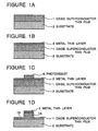
- Figures 1A to 1D illustrate the process for forming on a substrate an oxide superconductor thin filin having a central portion of 400nm thickness and opposite side portions of 100nm thickness, similarly to that formed in the conventional process explained hereinbefore.
- an oxide superconductor thin film 1 having a thickness of 400nm was formed on a substrate 2 by sputtering.
- a metal film 3 of 100nm thickness was formed on an upper surface of the oxide superconductor thin film 1 by a vacuum evaporation process.
- a photoresist mask 8 was formed on a central portion of the metal film 3.
- Ar-ion beam etching was performed using the photoresist layer 8 as a mask, until opposite side portions of the oxide superconductor thin film 1 have a thickness of 100nm, as shown in Figure 1D.
- a remaining photoresist mask 8 is ashed by using O2 plasma, so that the remaining photoresist mask 8 is completely removed. With removal of the remaining photoresist mask 8 by a dry process, the oxide superconductor thin film 1 will in no way be in contact with a photoresist removing liquid and a cleaning water.
- the oxide superconductor thin film having a thick portion 1A and a thin portion 1B is formed.
- a superconducting device is formed on or in the thick portion 1A, and the thin portion 1B constitutes a lower side electrode of the superconducting device, or a lead conductor from the thick portion 1A.
- an electrode or contact for connection is formed on the thin portion 1B.
- the oxide superconductor thin film 1 was formed of Y1Ba2Cu3O x oxide superconductor, Bi2Sr2Ca2Cu3O y oxide superconductor and Tl2Ba2Ca2Cu3O z oxide superconductor, respectively.
- a MgO single crystalline substrate (100) is used as the substrate 2.
- the metal film 3 was formed of Au (gold).
- oxide superconductor thin films having the same shape were formed in accordance with the conventional method explained hereinbefore, and the superconducting characteristics of these thin films were measured.
- the following table shows the superconducting characteristics of the oxide superconductor thin films worked in accordance with the present invention method and in accordance with the conventional method.
- the oxide superconductor thin films worked in accordance with the present invention method have the superconducting characteristics more excellent than the conventional ones.
- FIG. 2 there is shown a diagrammatic section view illustrating one example of a superconducting device formed by utilizing the method in accordance with the present invention.
- the superconducting device shown in Figure 2 is a so-called Josephson mixer.
- the shown device includes a first superconducting electrode 11 formed of Y1Ba2Cu3O x thin film formed on a MgO substrate 2, an Au thin layer 4 formed on a central portion of the first superconducting electrode 11, and a second superconducting electrode 12 formed of Y1Ba2Cu3O x thin film formed on the Au thin layer 4 without directly contacting with the first superconducting electrode 11.
- a pair of metal electrodes 5 and 6 are located on the second superconducting electrode 12.
- another pair of metal electrodes 7 and 8 having connecting terminals 17 and 18, respectively, are provided respectively on opposite end portions of the first superconducting electrode 11 on which the Au layer 4 is not formed.
- the metal electrodes 5 and 6 excluding an upper surface thereof are covered with an insulating layer 9, and metal layers 15 and 16 are formed on the insulating layer 9 so as to extend from the upper surfaces of the metal electrode 5 and 6 and to be connected to connecting terminals 27 and 28 in proximity of the metal electrodes 7 and 8, respectively.
- the maximum thickness of each of the first and second superconducting electroes 11 and 12 was 400nm, and the thickness of the Au layer 4 was 10nm.
- the metal electrodes 5 and 6 formed on the second superconducting electrode 12 were formed in a double-layered structure having an lower layer of Ag in contact with the second superconducting electrode 12 and an upper layer Au formed on the Ag lower layer. This double-layered metal electrode does not give an adverse influence to the compound oxide superconductor, and has an excellent adhesion or bonding property to the compound oxide superconductor.
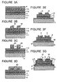
- a first Y1Ba2Cu3O x superconductor thin film 111, an Au layer 4, a second Y1Ba2Cu3O x superconductor thin film 112 and a metal layer 114 were formed on the MgO substrate 2 in the named order in such a manner that each layer completely covers an upper surface of a just-lower layer.
- the first Y1Ba2Cu3O x superconductor thin film 111 and the second Y1Ba2Cu3O x superconductor thin film 112 were deposited to have a thickness of 400nm by sputtering, respectively.
- the Au layer 4 was deposited to have a thickness of 10nm by vacuum evaporation.
- the metal layer 114 was formed by depositing an Ag layer of 150nm thickness by vacuum evaporation and also depositing an Au layer of 150nm thickness on the Ag layer by vacuum evaporation. Thereafter, a photoresist layer 8 is deposited on the metal layer 114, as shown in Figure 3A.
- the photoresist layer 114 was patterned so that resist masks 81 and 82 are left on portions of the metal layer 114 which become the metal electrodes in future.
- Ar-ion etching was performed by using the remaining resists 81 and 82 as a mask, so that the metal layer 114 not covered with the remaining resists 81 and 82 are completely removed.
- the metal electrodes 5 and 6 are formed as shown in Figure 3C.
- a photoresist layer 83 is deposited on the second Y1Ba2Cu3O x superconductor thin film 112 so as to cover the metal electrodes 5 and 6.
- Ar-ion etching was performed by using the photoresist 83 as a mask, so that the second Y1Ba2Cu3O x superconductor thin film 112 and the Au layer 4 which are not covered with the photoresist 83, were completely removed, and the first Y1Ba2Cu3O x superconductor thin film 111 which is not covered with the photoresist 83, was partially removed, with the result that the first superconducting electrode 11 and the second superconducting electrode 12 are formed as shown in Figure 3E.
- an insulating layer 9 is formed to cover portions excluding opposite end portions 37 and 38 of the first superconducting electrode 11 and an upper surface of each of the metal electrodes 5 and 6.
- metal electrodes 7 and 8 are formed on exposed opposite end portions 37 and 38 of the first superconducting electrode 11, and metal layers 15 and 16 are formed to cover the upper surface of the metal electrodes 5 and 6 and to extend from the upper surface of the metal electrodes 5 and 6 on the surface of the insulating layer 9.
- the superconducting device shown in Figure 2 is completed.
- the above mentioned superconducting device responded to a microwave of 9GHz and stably operated with a clear Shapiro step.
- the Au layer 4 can be replaced with a SrTiO3 layer of 1nm thickness.
- This superconducting device can be formed by depositing the SrTiO3 layer of 1nm thickness on the first Y1Ba2Cu3O x superconductor thin film 111 by sputtering, in place of depositing the Au layer 4, when the stacked structure illustrated in Figure 3A is formed.
- the method in accordance with the present invention can work an oxide superconductor thin film without deteriorating characteristics of the oxide superconductor. Therefore, the method in accordance with the present invention makes it easy to form a superconducting device by a fine working of a superconductor thin film, and therefore, utilization of superconduction technique is further facilitated.
Description
- The present invention relates to a method for manufacturing a superconductor device, and more specifically to a method for forming an oxide superconductor thin film having different thickness portions, in a process for manufacturing a superconductor device.
- In a process of manufacturing superconductor devices such as Josephson devices and superconductor transistors, it is necessary to form a superconductor in the form of a thin film, and to work the superconductor thin film into a desired shape.
- When a superconductor used in the superconductor devices is composed of an oxide superconductor such as Y-Ba-Cu-O oxide superconductor typified by Y₁Ba₂Cu₃Ox, Bi-Sr-Ca-Cu-O oxide superconductor typified by Bi₂Sr₂Ca₂Cu₃Oy, and Tl-Ba-Ca-Cu-O oxide superconductor typified by Tl₂Ba₂Ca₂Cu₃Oz, formation and working of the thin film have been performed as follows:
- In an ordinary practice, a thin film of an oxide superconductor is formed by using a physical vapor deposition process such as a sputtering and molecular beam epitaxy, or a chemical vapor deposition process such as metal organic chemical vapor deposition (MO-CVD). After formation of the thin film, a heat treatment can be performed in order to improve characteristics of the oxide superconductor thin film. Regardless of the kind of the thin film formation process, it is necessary to unify the crystal orientation in the formed oxide superconductor thin film. The reason for this is that the above mentioned oxide superconductor generally has directivity in superconduction critical current density.
- In the case of forming an oxide superconductor thin film having different thickness portions, a thin film having a thickness equal to the thickness of the thinnest thickness portion of the different thickness portions is first formed, and thereafter, a mask is deposited on a portion to be left as the thinnest portion, and an oxide superconductor is further deposited on the thin film having a thickness equal to the thinnest thickness.
- In the following, there will be explained an example of a conventional process for forming on a substrate an oxide superconductor thin film having a central portion of 400nm thickness and opposite side portions of 100nm thickness. First, an oxide superconductor thin film having a thickness of 100nm is formed on the substrate by sputtering or another process. A portion of the thus deposited oxide superconductor thin film other than a central portion is masked with a photoresist, and an oxide superconductor is further deposited by sputtering or another thickness, so that the central portion is constituted of an oxide superconductor thin film having a thickness of 400nm.
- As seen from the above, the conventional process is featured in which an oxide superconductor thin film having a thickness of the thinnest thickness portion is formed on a whole surface of the substrate, and thereafter, an unnecessary portion of the formed oxide superconductor thin film is covered with a mask and an oxide superconductor is selectively further deposited on only a required portion of the formed oxide superconductor thin film. As a result, the oxide superconductor thin film having different thickness portions is formed.
- The above mentioned process has been disadvantageous in that reaction occurs at an boundary between a photoresist used as the mask and a firstly formed oxide superconductor thin film, so that the characteristics of the oxide superconductor is deteriorated. In a photolithography process, a surface of the first formed oxide superconductor thin film is in contact with an alkaline developing liquid, a resist removing liquid and a cleaning water. An upper oxide superconductor layer is deposited on the surface of the lower oxide superconductor thin film which had once been in contact with these kinds of liquid. In this case, a discontinuous boundary is formed between the upper oxide superconductor layer and the lower oxide superconductor thin film, and a uniform oxide superconductor thin film having a thick portion and a thin portion cannot be obtained.
- European patent application n° 0 366 949, which is a document under Article 54(3) EPC, discloses a method for forming a superconducting device having different thickness portions, said method comprising the step of depositing on a substrate a first superconducting thin film, forming a barrier layer on said superconducting thin film, forming a second superconducting film on said barrier layer and etching said second superconducting film and portions of said first superconducting film with an Ar-ion beam.
- Journal of Physics D, Applied Physics, Vol 20, N° 10 (1987) pp. 1330-1335, discloses a method for forming a superconducting device having different thickness portions, said method comprising a first step of etching a Nb layer deposited on a superconducting double film using a CF4 plasma, and a second step of milling the superconducting double film to portions of different thickness using an Ar-ion beam.
- Accordingly, it is an object of the present invention to provide a method for working an oxide superconductor thin film without deteriorating characteristics of the oxide superconductor, which method has overcome the above mentioned defects in the conventional oxide superconductor device manufacturing process.
- The above and other objects of the present invention are achieved in accordance with the present invention by, a process of manufacturing a superconductor device, comprising a method of forming an oxide superconductor thin film having different thickness portions, wherein said oxide superconductor thin film is coated with a metal layer, characterised in that the method includes the step of etching together said oxide supercondutor thin film and said metal layer by means of photolithographic patterning so that the oxide superconductor thin film has a thin thickness portion.
- According to another aspect of the present invention, an oxide superconductor thin film is formed on a substrate, and a portion of the oxide superconductor thin film formed on the substrate is etched so that a convex portion having a thickness larger than a peripheral thin portion and having a contour defined by the peripheral thin portion is formed. At least a portion of an oxide superconductor thin film device is formed in the convex portion.
- The above mentioned method in accordance with the present invention is characterized in that only a portion of a relatively thick oxide superconductor thin film formed on a whole is etched so as to have a reduced thickness, in order to form an oxide superconductor thin film having different thickness portions in the process for manufacturing a superconductor device. Accordingly, in the case of forming an oxide superconductor thin film having different thickness portions on a given surface in accordance with the present invention, growth of an oxide superconductor thin film on the given surface can be performed in one step. Namely, an oxide superconductor thin film having a thickness equal to that of the thickest portion of the oxide superconductor thin film having different thickness portions is formed with the one step. Thereafter, a thin portion and/or unnecessary portion is formed or removed by electively etching the oxide superconductor thin film having the thickness equal to that of the thickest portion.
- The fact that the growth of an oxide superconductor thin film on the given surface is performed in one step, means that a single continuous or integral layer or sheet of an oxide superconductor thin film is grown in one step. Therefore, for a structure in which a non-superconductor is integrally sandwiched between a pair of superconductor thin films, for example a tunnel junction type superconducting weak link structure, a required number of superconductor thin films are formed in a single continuous step. In addition, in the oxide superconductor thin film of a stacked-layer structure in which a plurality of layers of oxide superconductor thin films and a non-superconductor thin film are stacked, these layers are preferably formed in a manner that the substrate is never taken out of a chamber of a film formation or deposition device until an uppermost layer is deposited, so that the oxide superconductor will never be contacted with air in the course of the oxide superconductor thin film formation process.
- In the method in accordance with the present invention, since the growth of the thin film is performed in one step, a uniform oxide superconductor thin film having a good crystalline condition can be obtained. Therefore, in case of forming a junction such as superconducting weak link junction between an oxide superconductor thin film and another thin film, not only a uniform oxide superconductor thin film having a good crystalline condition can be obtained, but also a good boundary can be formed at the junction portion.
- The superconduction property of the oxide suporconductor thin film is greatly influenced by a crystalline orientation and composition. Therefore, an oxide superconductor thin film formed by many times of separate deposition cannot have a continuous crystal, and a boundary adversely occurs, with the result that a uniform superconduction property cannot be obtained. Needless to say, this oxide superconductor thin film is not suitable to form a superconducting weak link junction. The characteristics of the superconducting weak link junction is also greatly influenced by a condition of boundary in the junction portion. Particularly, if a surface or portion to be brought into the boundary is contacted with air in the manufacturing process and the surface condition is caused to adversely change, a desired characteristics of the superconducting weak link junction cannot be obtained. However, if the method in accordance with the present invention is used, this problem can be overcome.
- The method in accordance with the present invention can be applied to any type of oxide superconductor. For example, the present invention can be applied to Y-Ba-Cu-O oxide superconductor typified by Y₁Ba₂Cu₃Ox (6<x≤7), Bi-Sr-Ca-Cu-O oxide superconductor typified by Bi₂Sr₂Ca₂Cu₃Oy (7≤y≤10), and Tl-Ba-Ca-Cu-O oxide superconductor typified by Tl₂Ba₂Ca₂Cu₃Oz (7≤z≤10). However, it should be noted that the present invention is in no way limited to these oxide superconductors.
- Furthermore, in the method of the present invention, the etching is preferably performed by a dry etching process, for example, an ion beam etching using inert gas such as Ar (argon), an ECR (electron cycroton resonance) etching, an RF (radio frequency) plasma etching, etc. These etching processes are very preferable, since a physical etching is realized by charged particles without chemical reaction, and therefore with less influence to the oxide superconductor. In the case of the Ar ion beam etching, an acceleration voltage for Ar-ions is preferred to be in a range of 600 V to 800 V. If the acceleration voltage is less than 600 V, the time for etching becomes too long, and if the acceleration voltage is greater than 800 V, the oxide superconductor crystal of a region in proximity of a surface is destroyed.
- In the method of the present invention, after formation of the uniform oxide superconductor thin film, a surface of the oxide superconductor thin film is preferably protected by covering the thin film surface with a film of metal which does not give an adverse influence to the oxide superconductor. This is particularly advantageous in the case of performing the etching after patterning a mask by use of a photolithography. If the oxide superconductor thin film surface is covered with the metal film, the oxide superconductor thin film will never be contacted with an alkaline developing liquid, a resist removing liquid and a cleaning water which are used in the photolithography process of the mask patterning. Therefore, even after the shaping of the oxide superconductor thin film, the superconducting characteristics will be not deteriorated. The metal used as the protection metal film is preferably Ag (silver), since Ag is remarkably low in reactivity to the oxide superconductor, and since Ag has a low contact resistance with the oxide superconductor and an excellent adhesion or bonding property to the oxide superconductor. However, it is possible to use, as the metal for the protection metal film, a metal material having a low reactivity to oxide superconductors, for example, Al, In, Zn, Cu, Ni, Au, Pt, Ti, Pd, etc. In addition, the protection metal film can be formed by means of an evaporation process.
- The above and other objects, features and advantages of the present invention will be apparent from the following description of preferred embodiments of the invention with reference to the accompanying drawings. However, the examples explained hereinafter are only for illustration of the present invention, and therefore, it should be understood that the present invention is in no way limited to the following examples.
-
- Figures 1A to 1D are diagrammatic section views illustrating the process in accordance with the present invention for working an oxide superconductor thin film;
- Figure 2 is a diagrammatic section view illustrating one example of a superconducting device formed by utilizing the method in accordance with the present invention; and
- Figures 3A to 3G are diagrammatic section views illustrating the process for manufacturing the superconducting device shown in Figure 2.
- Oxide superconductor thin films were worked in accordance with the method of the present invention, and superconducting characteristics of the worked oxide superconductor thin films was measured.
- First, the process of the method of the present invention will be described with reference to Figures 1A to 1D, which illustrate the process for forming on a substrate an oxide superconductor thin filin having a central portion of 400nm thickness and opposite side portions of 100nm thickness, similarly to that formed in the conventional process explained hereinbefore.
- First, as shown in Figure 1A, an oxide superconductor
thin film 1 having a thickness of 400nm was formed on asubstrate 2 by sputtering. As shown in Figure 1B, ametal film 3 of 100nm thickness was formed on an upper surface of the oxide superconductorthin film 1 by a vacuum evaporation process. Thereafter, as shown in Figure 1C, aphotoresist mask 8 was formed on a central portion of themetal film 3. Then, Ar-ion beam etching was performed using thephotoresist layer 8 as a mask, until opposite side portions of the oxide superconductorthin film 1 have a thickness of 100nm, as shown in Figure 1D. - A remaining
photoresist mask 8 is ashed by using O₂ plasma, so that the remainingphotoresist mask 8 is completely removed. With removal of the remainingphotoresist mask 8 by a dry process, the oxide superconductorthin film 1 will in no way be in contact with a photoresist removing liquid and a cleaning water. - Thus, the oxide superconductor thin film having a
thick portion 1A and athin portion 1B is formed. For example, a superconducting device is formed on or in thethick portion 1A, and thethin portion 1B constitutes a lower side electrode of the superconducting device, or a lead conductor from thethick portion 1A. In this case, an electrode or contact for connection is formed on thethin portion 1B. - The oxide superconductor
thin film 1 was formed of Y₁Ba₂Cu₃Ox oxide superconductor, Bi₂Sr₂Ca₂Cu₃Oy oxide superconductor and Tl₂Ba₂Ca₂Cu₃Oz oxide superconductor, respectively. A MgO single crystalline substrate (100) is used as thesubstrate 2. Themetal film 3 was formed of Au (gold). - For comparison, oxide superconductor thin films having the same shape were formed in accordance with the conventional method explained hereinbefore, and the superconducting characteristics of these thin films were measured. The following table shows the superconducting characteristics of the oxide superconductor thin films worked in accordance with the present invention method and in accordance with the conventional method.
Superconductor Thin Film Tc(K) Jc (A/cm) Invention Y₁Ba₂Cu₃Ox 89 1.0 × 10⁶ Bi₂Sr₂Ca₂Cu₃Oy 103 7.0 × 10⁵ Tl₂Ba₂Ca₂Cu₃Oz 110 3.8 × 10⁵ Comparative Y₁Ba₂Cu₃Ox 79 4.0 × 10⁵ Bi₂Sr₂Ca₂Cu₃Oy 80 1.0 × 10⁵ Tl₂Ba₂Ca₂Cu₃Oz 90 3.0 × 10⁴ - As seen from the above table, the oxide superconductor thin films worked in accordance with the present invention method have the superconducting characteristics more excellent than the conventional ones.
- Referring to Figure 2, there is shown a diagrammatic section view illustrating one example of a superconducting device formed by utilizing the method in accordance with the present invention. The superconducting device shown in Figure 2 is a so-called Josephson mixer. The shown device includes a first
superconducting electrode 11 formed of Y₁Ba₂Cu₃Ox thin film formed on aMgO substrate 2, an Authin layer 4 formed on a central portion of the firstsuperconducting electrode 11, and a secondsuperconducting electrode 12 formed of Y₁Ba₂Cu₃Ox thin film formed on the Authin layer 4 without directly contacting with the firstsuperconducting electrode 11. A pair ofmetal electrodes superconducting electrode 12. In addition, another pair ofmetal electrodes 7 and 8 having connecting terminals 17 and 18, respectively, are provided respectively on opposite end portions of the firstsuperconducting electrode 11 on which theAu layer 4 is not formed. Themetal electrodes layer 9, andmetal layers layer 9 so as to extend from the upper surfaces of themetal electrode terminals 27 and 28 in proximity of themetal electrodes 7 and 8, respectively. - In the above mentioned superconducting device, the maximum thickness of each of the first and
second superconducting electroes Au layer 4 was 10nm. In addition, themetal electrodes superconducting electrode 12 were formed in a double-layered structure having an lower layer of Ag in contact with the secondsuperconducting electrode 12 and an upper layer Au formed on the Ag lower layer. This double-layered metal electrode does not give an adverse influence to the compound oxide superconductor, and has an excellent adhesion or bonding property to the compound oxide superconductor. - Now, a process for forming the above mentioned superconducting device will be explained with reference to Figures 3A to 3G.
- As shown in Figure 3A, a first Y₁Ba₂Cu₃Ox superconductor
thin film 111, anAu layer 4, a second Y₁Ba₂Cu₃Ox superconductorthin film 112 and ametal layer 114 were formed on theMgO substrate 2 in the named order in such a manner that each layer completely covers an upper surface of a just-lower layer. The first Y₁Ba₂Cu₃Ox superconductorthin film 111 and the second Y₁Ba₂Cu₃Ox superconductorthin film 112 were deposited to have a thickness of 400nm by sputtering, respectively. TheAu layer 4 was deposited to have a thickness of 10nm by vacuum evaporation. Themetal layer 114 was formed by depositing an Ag layer of 150nm thickness by vacuum evaporation and also depositing an Au layer of 150nm thickness on the Ag layer by vacuum evaporation. Thereafter, aphotoresist layer 8 is deposited on themetal layer 114, as shown in Figure 3A. - Then, as shown in Figure 3B, the
photoresist layer 114 was patterned so that resist masks 81 and 82 are left on portions of themetal layer 114 which become the metal electrodes in future. Ar-ion etching was performed by using the remaining resists 81 and 82 as a mask, so that themetal layer 114 not covered with the remaining resists 81 and 82 are completely removed. As a result, themetal electrodes - Thereafter, as shown in Figure 3D, a
photoresist layer 83 is deposited on the second Y₁Ba₂Cu₃Ox superconductorthin film 112 so as to cover themetal electrodes photoresist 83 as a mask, so that the second Y₁Ba₂Cu₃Ox superconductorthin film 112 and theAu layer 4 which are not covered with thephotoresist 83, were completely removed, and the first Y₁Ba₂Cu₃Ox superconductorthin film 111 which is not covered with thephotoresist 83, was partially removed, with the result that the firstsuperconducting electrode 11 and the secondsuperconducting electrode 12 are formed as shown in Figure 3E. - Furthermore, as shown in Figure 3F, an insulating
layer 9 is formed to cover portions excludingopposite end portions superconducting electrode 11 and an upper surface of each of themetal electrodes - As shown in Figure 3G,
metal electrodes 7 and 8 are formed on exposedopposite end portions superconducting electrode 11, andmetal layers metal electrodes metal electrodes layer 9. Thus, the superconducting device shown in Figure 2 is completed. - At a temperature of 40K, the above mentioned superconducting device responded to a microwave of 9GHz and stably operated with a clear Shapiro step.
- In the superconducting device shown in Figure 2, the
Au layer 4 can be replaced with a SrTiO₃ layer of 1nm thickness. This superconducting device can be formed by depositing the SrTiO₃ layer of 1nm thickness on the first Y₁Ba₂Cu₃Ox superconductorthin film 111 by sputtering, in place of depositing theAu layer 4, when the stacked structure illustrated in Figure 3A is formed. - As seen from the above description, the method in accordance with the present invention can work an oxide superconductor thin film without deteriorating characteristics of the oxide superconductor. Therefore, the method in accordance with the present invention makes it easy to form a superconducting device by a fine working of a superconductor thin film, and therefore, utilization of superconduction technique is further facilitated.
- The invention has thus been shown and described with reference to the specific embodiments. However, it should be noted that the present invention is in no way limited to the details of the illustrated structures but changes and modifications may be made within the scope of the appended claims.
Claims (9)
- A process of manufacturing a superconductor device, comprising a method of forming an oxide superconductor thin film having different thickness portions, wherein said oxide superconductor thin film is coated with a metal layer, characterised in that the method includes the step of etching together said oxide superconductor thin film and said metal layer by means of photolithographic patterning so that the oxide superconductor thin film has a thin thickness portion.
- A method claimed in Claim 1 wherein said oxide superconductor thin film is formed in a single thin film growth process.
- A method claimed in Claim 1 wherein said oxide superconductor thin film is continuously formed without being taken out of a thin film deposition apparatus.
- A method claimed in any of claims 1 to 3 wherein said etching is performed by using a physical dry etching.
- A method claimed in Claim 4 wherein said physical dry etching is Ar-ion beam etching.
- A method claimed in Claim 5 wherein an Ar-ion acceleration voltage for said Ar-ion beam etching is in the range of 600V to 800V.
- A method claimed in any of Claims 1 to 6 wherein said oxide superconductor thin film is composed of Y₁Ba₂Cu₃Ox (6<x≤7), Bi₂Sr₂Ca₂Cu₃Oy (7≤y≤10), or Tl₂Ba₂Ca₂Cu₃Oz (7≤z≤10).
- A method claimed in any of Claims 1 to 7 wherein said oxide superconductor thin film is formed on a substrate, and wherein a portion of the oxide superconductor thin film formed on the substrate is etched so that a convex portion having a thickness larger than a peripheral thin portion and having a contour defined by the peripheral thin portion is formed, and at least a portion of an oxide superconductor thin film device is formed in said convex portion.
- A method claimed in any of Claims 1 to 8 wherein said oxide superconductor thin film has a uniform thickness and a portion of said oxide superconductor thin film having the uniform thickness is etch-removed so that said oxide superconductor thin film has a portion thinner than the uniform thickness.
Applications Claiming Priority (4)
| Application Number | Priority Date | Filing Date | Title |
|---|---|---|---|
| JP1261491A JPH03124077A (en) | 1989-10-06 | 1989-10-06 | Manufacture of superconducting element |
| JP261491/89 | 1989-10-06 | ||
| JP296740/89 | 1989-11-15 | ||
| JP1296740A JPH03156983A (en) | 1989-11-15 | 1989-11-15 | Superconducting device |
Publications (3)
| Publication Number | Publication Date |
|---|---|
| EP0421889A2 EP0421889A2 (en) | 1991-04-10 |
| EP0421889A3 EP0421889A3 (en) | 1991-12-11 |
| EP0421889B1 true EP0421889B1 (en) | 1996-03-27 |
Family
ID=26545106
Family Applications (1)
| Application Number | Title | Priority Date | Filing Date |
|---|---|---|---|
| EP90402787A Expired - Lifetime EP0421889B1 (en) | 1989-10-06 | 1990-10-08 | Method for forming a continuous oxide superconductor layer having different thickness portions for superconductor device |
Country Status (4)
| Country | Link |
|---|---|
| US (1) | US5418213A (en) |
| EP (1) | EP0421889B1 (en) |
| CA (1) | CA2027067C (en) |
| DE (1) | DE69026179T2 (en) |
Families Citing this family (15)
| Publication number | Priority date | Publication date | Assignee | Title |
|---|---|---|---|---|
| JPH03270280A (en) * | 1990-03-09 | 1991-12-02 | Univ California | Microelectron circuit element having superconductive crosspath and manu- facture thereof |
| CA2443792A1 (en) * | 2002-10-08 | 2004-04-08 | Bayer Healthcare Llc | Method and systems for data management in patient diagnoses and treatment |
| US7521932B2 (en) | 2003-05-06 | 2009-04-21 | The Penn State Research Foundation | Method and system for adjusting the fundamental symmetric mode of coupled high temperature superconductor coils |
| US7295085B2 (en) * | 2003-08-21 | 2007-11-13 | E.I. Du Pont De Nemours And Company | Process for making high temperature superconductor devices each having a line oriented in a spiral fashion |
| US20070245374A1 (en) * | 2003-11-24 | 2007-10-18 | Inventec Corporation | Video program subtitle tex recording method and system |
| US7332910B2 (en) * | 2003-11-24 | 2008-02-19 | E.I. Du Pont De Nemours And Company | Frequency detection system comprising circuitry for adjusting the resonance frequency of a high temperature superconductor self-resonant coil |
| US7301344B2 (en) | 2003-11-24 | 2007-11-27 | E.I. Du Pont De Nemours & Co. | Q-damping circuit including a high temperature superconductor coil for damping a high temperature superconductor self-resonant coil in a nuclear quadrupole resonance detection system |
| US7375525B2 (en) * | 2003-12-15 | 2008-05-20 | E.I. Du Pont De Nemours And Company | Use of multiple sensors in a nuclear quadropole resonance detection system to improve measurement speed |
| WO2005078469A1 (en) * | 2004-02-04 | 2005-08-25 | E.I. Dupont De Nemours And Company | The use of two or more sensors to detect different nuclear quadrupole resonance signals of a target compound |
| WO2005109023A2 (en) * | 2004-02-04 | 2005-11-17 | E.I. Dupont De Nemours And Company | Nqr rf coil assembly comprising two or more coils which may be made from hts |
| US7279897B2 (en) * | 2004-04-30 | 2007-10-09 | E. I. Du Pont De Nemours And Company | Scanning a band of frequencies using an array of high temperature superconductor sensors tuned to different frequencies |
| US7265549B2 (en) | 2004-04-30 | 2007-09-04 | E. I. Du Pont De Nemours And Company | Scanning a band of frequencies using an array of high temperature superconductor sensors tuned to the same frequency |
| WO2006073452A2 (en) * | 2004-04-30 | 2006-07-13 | E.I. Dupont De Nemours And Company | Methods and apparatus for scanning a band of frequencies by nqr using an array of high temperature superconductor sensors |
| EP1825288A2 (en) * | 2004-12-03 | 2007-08-29 | E.I. Dupont De Nemours And Company | Matual decoupling of excitation and receive coils of a nuclear quadrupole resonance detection system |
| EP1831714A1 (en) * | 2004-12-13 | 2007-09-12 | E.I. Dupont De Nemours And Company | Metal shield alarm in a nuclear quadrupole resonance/x-ray contraband detection system |
Family Cites Families (3)
| Publication number | Priority date | Publication date | Assignee | Title |
|---|---|---|---|---|
| US5047390A (en) * | 1988-10-03 | 1991-09-10 | Matsushita Electric Industrial Co., Ltd. | Josephson devices and process for manufacturing the same |
| US5041188A (en) * | 1989-03-02 | 1991-08-20 | Santa Barbara Research Center | High temperature superconductor detector fabrication process |
| DE69026301T2 (en) * | 1989-05-12 | 1996-09-05 | Matsushita Electric Ind Co Ltd | Superconducting device and its manufacturing process |
-
1990
- 1990-10-05 CA CA002027067A patent/CA2027067C/en not_active Expired - Fee Related
- 1990-10-08 EP EP90402787A patent/EP0421889B1/en not_active Expired - Lifetime
- 1990-10-08 DE DE69026179T patent/DE69026179T2/en not_active Expired - Fee Related
-
1993
- 1993-05-18 US US08/064,331 patent/US5418213A/en not_active Expired - Fee Related
Also Published As
| Publication number | Publication date |
|---|---|
| EP0421889A3 (en) | 1991-12-11 |
| DE69026179T2 (en) | 1996-10-10 |
| DE69026179D1 (en) | 1996-05-02 |
| CA2027067A1 (en) | 1991-04-07 |
| CA2027067C (en) | 1996-07-23 |
| US5418213A (en) | 1995-05-23 |
| EP0421889A2 (en) | 1991-04-10 |
Similar Documents
| Publication | Publication Date | Title |
|---|---|---|
| EP0421889B1 (en) | Method for forming a continuous oxide superconductor layer having different thickness portions for superconductor device | |
| US6066600A (en) | Method of making high-Tc SSNS and SNS Josephson junction | |
| US5801393A (en) | Superconductor-insulator-superconductor Josephson tunnel junction and method therefor | |
| EP0545816B1 (en) | Method for manufacturing a Josephson junction device having weak link of artificial grain boundary | |
| EP0545801B1 (en) | Superconducting device having an extremely thin superconducting channel formed of oxide superconductor material and method for manufacturing the same | |
| EP0572324B1 (en) | Josephson junction device formed of oxide superconductor and process for preparing the same | |
| EP0612114B1 (en) | Method for forming a patterned oxide superconductor thin film | |
| EP0660428B1 (en) | Method for forming a step on a deposition surface of a substrate for a superconducting device utilizing an oxide superconductor | |
| US5506197A (en) | Superconducting device having an extremely thin superconducting channel formed of oxide superconductor material | |
| EP0419361B2 (en) | Method for forming an electrode for electrical connection to oxide superconductor | |
| EP0546904B1 (en) | Method for manufacturing an artificial grain boundary type Josephson junction device | |
| EP0573340A1 (en) | Josephson junction device formed of oxide superconductor | |
| EP0551033B1 (en) | Superconducting device having an extremely thin superconducting channel formed of oxide superconductor material and method for manufacturing the same | |
| EP0484232B1 (en) | Superconducting device having an extremely short superconducting channel formed of oxide superconductor material and method for manufacturing the same | |
| EP0546957B1 (en) | Superconducting device having an extremely thin superconducting channel formed of oxide superconductor material and method for manufacturing the same | |
| EP0508844B1 (en) | Superconducting thin film having at least one isolated superconducting region formed of oxide superconductor material and method for manufacturing the same | |
| US5721196A (en) | Stacked tunneling and stepped grain boundary Josephson junction | |
| EP0422641B1 (en) | Superconductor device | |
| EP0533519B1 (en) | Superconducting device having an extremely thin superconducting channel formed of oxide superconductor material and method for manufacturing the same | |
| US5247189A (en) | Superconducting device composed of oxide superconductor material | |
| EP0546959B1 (en) | Superconducting device having an extremely thin superconducting channel formed of oxide superconductor material | |
| EP0545815B1 (en) | Josephson junction device formed of oxide superconductor material and process for preparing the same | |
| EP0509886B1 (en) | Process for patterning layered thin films including a superconductor layer | |
| EP0557207A1 (en) | Josephson junction device of oxide superconductor and process for preparing the same | |
| JPH03124077A (en) | Manufacture of superconducting element |
Legal Events
| Date | Code | Title | Description |
|---|---|---|---|
| PUAI | Public reference made under article 153(3) epc to a published international application that has entered the european phase |
Free format text: ORIGINAL CODE: 0009012 |
|
| 17P | Request for examination filed |
Effective date: 19901221 |
|
| AK | Designated contracting states |
Kind code of ref document: A2 Designated state(s): DE FR GB IT NL |
|
| PUAL | Search report despatched |
Free format text: ORIGINAL CODE: 0009013 |
|
| AK | Designated contracting states |
Kind code of ref document: A3 Designated state(s): DE FR GB IT NL |
|
| 17Q | First examination report despatched |
Effective date: 19940222 |
|
| GRAA | (expected) grant |
Free format text: ORIGINAL CODE: 0009210 |
|
| AK | Designated contracting states |
Kind code of ref document: B1 Designated state(s): DE FR GB IT NL |
|
| REF | Corresponds to: |
Ref document number: 69026179 Country of ref document: DE Date of ref document: 19960502 |
|
| ITF | It: translation for a ep patent filed |
Owner name: AVV. ANTONIO PETRUZZELLI |
|
| ET | Fr: translation filed | ||
| PLBE | No opposition filed within time limit |
Free format text: ORIGINAL CODE: 0009261 |
|
| STAA | Information on the status of an ep patent application or granted ep patent |
Free format text: STATUS: NO OPPOSITION FILED WITHIN TIME LIMIT |
|
| 26N | No opposition filed | ||
| REG | Reference to a national code |
Ref country code: GB Ref legal event code: IF02 |
|
| PGFP | Annual fee paid to national office [announced via postgrant information from national office to epo] |
Ref country code: GB Payment date: 20021002 Year of fee payment: 13 |
|
| PGFP | Annual fee paid to national office [announced via postgrant information from national office to epo] |
Ref country code: FR Payment date: 20021008 Year of fee payment: 13 |
|
| PGFP | Annual fee paid to national office [announced via postgrant information from national office to epo] |
Ref country code: DE Payment date: 20021011 Year of fee payment: 13 |
|
| PGFP | Annual fee paid to national office [announced via postgrant information from national office to epo] |
Ref country code: NL Payment date: 20021031 Year of fee payment: 13 |
|
| PG25 | Lapsed in a contracting state [announced via postgrant information from national office to epo] |
Ref country code: GB Free format text: LAPSE BECAUSE OF NON-PAYMENT OF DUE FEES Effective date: 20031008 |
|
| PG25 | Lapsed in a contracting state [announced via postgrant information from national office to epo] |
Ref country code: NL Free format text: LAPSE BECAUSE OF NON-PAYMENT OF DUE FEES Effective date: 20040501 Ref country code: DE Free format text: LAPSE BECAUSE OF NON-PAYMENT OF DUE FEES Effective date: 20040501 |
|
| GBPC | Gb: european patent ceased through non-payment of renewal fee |
Effective date: 20031008 |
|
| PG25 | Lapsed in a contracting state [announced via postgrant information from national office to epo] |
Ref country code: FR Free format text: LAPSE BECAUSE OF NON-PAYMENT OF DUE FEES Effective date: 20040630 |
|
| NLV4 | Nl: lapsed or anulled due to non-payment of the annual fee |
Effective date: 20040501 |
|
| REG | Reference to a national code |
Ref country code: FR Ref legal event code: ST |
|
| PG25 | Lapsed in a contracting state [announced via postgrant information from national office to epo] |
Ref country code: IT Free format text: LAPSE BECAUSE OF NON-PAYMENT OF DUE FEES;WARNING: LAPSES OF ITALIAN PATENTS WITH EFFECTIVE DATE BEFORE 2007 MAY HAVE OCCURRED AT ANY TIME BEFORE 2007. THE CORRECT EFFECTIVE DATE MAY BE DIFFERENT FROM THE ONE RECORDED. Effective date: 20051008 |