EP0484232B1 - Superconducting device having an extremely short superconducting channel formed of oxide superconductor material and method for manufacturing the same - Google Patents
Superconducting device having an extremely short superconducting channel formed of oxide superconductor material and method for manufacturing the same Download PDFInfo
- Publication number
- EP0484232B1 EP0484232B1 EP91402900A EP91402900A EP0484232B1 EP 0484232 B1 EP0484232 B1 EP 0484232B1 EP 91402900 A EP91402900 A EP 91402900A EP 91402900 A EP91402900 A EP 91402900A EP 0484232 B1 EP0484232 B1 EP 0484232B1
- Authority
- EP
- European Patent Office
- Prior art keywords
- superconducting
- thin film
- oxide
- substrate
- oxide superconductor
- Prior art date
- Legal status (The legal status is an assumption and is not a legal conclusion. Google has not performed a legal analysis and makes no representation as to the accuracy of the status listed.)
- Expired - Lifetime
Links
- 239000002887 superconductor Substances 0.000 title claims description 126
- 238000000034 method Methods 0.000 title claims description 42
- 239000000463 material Substances 0.000 title claims description 32
- 238000004519 manufacturing process Methods 0.000 title claims description 19
- 239000010409 thin film Substances 0.000 claims description 92
- 239000000758 substrate Substances 0.000 claims description 63
- 239000004065 semiconductor Substances 0.000 claims description 22
- 238000000151 deposition Methods 0.000 claims description 20
- 230000008021 deposition Effects 0.000 claims description 20
- 239000012212 insulator Substances 0.000 claims description 20
- 150000001875 compounds Chemical class 0.000 claims description 9
- 238000004544 sputter deposition Methods 0.000 claims description 9
- XUIMIQQOPSSXEZ-UHFFFAOYSA-N Silicon Chemical compound [Si] XUIMIQQOPSSXEZ-UHFFFAOYSA-N 0.000 claims description 6
- 229910052710 silicon Inorganic materials 0.000 claims description 4
- 239000010703 silicon Substances 0.000 claims description 4
- 229910015901 Bi-Sr-Ca-Cu-O Inorganic materials 0.000 claims description 3
- 229910002480 Cu-O Inorganic materials 0.000 claims description 3
- QPLDLSVMHZLSFG-UHFFFAOYSA-N Copper oxide Chemical compound [Cu]=O QPLDLSVMHZLSFG-UHFFFAOYSA-N 0.000 claims description 2
- 239000005751 Copper oxide Substances 0.000 claims description 2
- 229910000431 copper oxide Inorganic materials 0.000 claims description 2
- 229960004643 cupric oxide Drugs 0.000 claims description 2
- 238000005304 joining Methods 0.000 claims description 2
- 229910009203 Y-Ba-Cu-O Inorganic materials 0.000 claims 1
- 239000011810 insulating material Substances 0.000 claims 1
- 230000008569 process Effects 0.000 description 18
- 238000005530 etching Methods 0.000 description 14
- 239000010408 film Substances 0.000 description 8
- 230000000694 effects Effects 0.000 description 4
- 238000001451 molecular beam epitaxy Methods 0.000 description 4
- 238000010884 ion-beam technique Methods 0.000 description 3
- 229910002113 barium titanate Inorganic materials 0.000 description 2
- 230000004888 barrier function Effects 0.000 description 2
- 239000004020 conductor Substances 0.000 description 2
- 238000002161 passivation Methods 0.000 description 2
- 238000000059 patterning Methods 0.000 description 2
- 238000001020 plasma etching Methods 0.000 description 2
- 239000003870 refractory metal Substances 0.000 description 2
- 229910021332 silicide Inorganic materials 0.000 description 2
- FVBUAEGBCNSCDD-UHFFFAOYSA-N silicide(4-) Chemical compound [Si-4] FVBUAEGBCNSCDD-UHFFFAOYSA-N 0.000 description 2
- 238000000992 sputter etching Methods 0.000 description 2
- 238000007738 vacuum evaporation Methods 0.000 description 2
- 239000011248 coating agent Substances 0.000 description 1
- 238000000576 coating method Methods 0.000 description 1
- 239000000470 constituent Substances 0.000 description 1
- 239000013078 crystal Substances 0.000 description 1
- 230000007547 defect Effects 0.000 description 1
- 230000005684 electric field Effects 0.000 description 1
- 238000005516 engineering process Methods 0.000 description 1
- 238000001704 evaporation Methods 0.000 description 1
- 230000008020 evaporation Effects 0.000 description 1
- 230000005669 field effect Effects 0.000 description 1
- 238000009413 insulation Methods 0.000 description 1
- 238000012986 modification Methods 0.000 description 1
- 230000004048 modification Effects 0.000 description 1
- 238000000926 separation method Methods 0.000 description 1
Images


Classifications
-
- H—ELECTRICITY
- H10—SEMICONDUCTOR DEVICES; ELECTRIC SOLID-STATE DEVICES NOT OTHERWISE PROVIDED FOR
- H10N—ELECTRIC SOLID-STATE DEVICES NOT OTHERWISE PROVIDED FOR
- H10N60/00—Superconducting devices
- H10N60/20—Permanent superconducting devices
- H10N60/205—Permanent superconducting devices having three or more electrodes, e.g. transistor-like structures
- H10N60/207—Field effect devices
-
- Y—GENERAL TAGGING OF NEW TECHNOLOGICAL DEVELOPMENTS; GENERAL TAGGING OF CROSS-SECTIONAL TECHNOLOGIES SPANNING OVER SEVERAL SECTIONS OF THE IPC; TECHNICAL SUBJECTS COVERED BY FORMER USPC CROSS-REFERENCE ART COLLECTIONS [XRACs] AND DIGESTS
- Y10—TECHNICAL SUBJECTS COVERED BY FORMER USPC
- Y10S—TECHNICAL SUBJECTS COVERED BY FORMER USPC CROSS-REFERENCE ART COLLECTIONS [XRACs] AND DIGESTS
- Y10S505/00—Superconductor technology: apparatus, material, process
- Y10S505/825—Apparatus per se, device per se, or process of making or operating same
- Y10S505/873—Active solid-state device
Definitions
- the present invention relates to a superconducting device and a method for manufacturing the same, and more specifically to a superconducting device including an extremely short superconducting channel formed of oxide superconductor material, and a method for manufacturing the same.
- Typical three-terminal devices which utilize a superconductor include a so called superconducting-base transistor and a so called super-FET (field effect transistor).
- the superconducting-base transistor includes an emitter of a superconductor or a normal conductor, a tunnel barrier of an insulator, a base of a superconductor, a semiconductor isolator and a collector of a normal conductor, stacked in the named order.
- This superconducting-base transistor operates at a high speed with a low power consumption, by utilizing high speed electrons passing through the tunnel barrier.
- the super-FET includes a semiconductor layer, and a superconductor source electrode and a superconductor drain electrode which are formed closely to each other on the semiconductor layer.
- a portion of the semiconductor layer between the superconductor source electrode and the superconductor drain electrode has a greatly recessed or undercut war surface so as to have a reduced thickness.
- a gate electrode is formed through a gate insulating layer on the recessed or undercut rear surface of the portion of the semiconductor layer between the superconductor source electrode and the superconductor drain electrode.
- a superconducting current flows through the semiconductor layer portion between the superconductor source electrode and the superconductor drain electrode due to a proximity effect, and is controlled by an applied gate voltage.
- This super-FET also operates at a high speed with a low power consumption, (see for example IBM Technical Disclosure Bulletin, Vol. 32, No 3A, August 1989, pp. 77-78).
- Both of the above mentioned superconducting-base transistor and the super-FET have a portion in which a semiconductor layer and a superconducting layer are stacked to each other.
- the superconductor source electrode and the superconductor drain electrode have to be located close to each other at a distance which is not greater than a few times the coherence length of the superconductor materials of the superconductor source electrode and the superconductor drain electrode.
- the oxide superconductor has a short coherence length
- a distance between the superconductor source electrode and the superconductor drain electrode has to be not greater than a few ten nanometers.
- it is very difficult to conduct a fine processing such as a fine pattern etching so as to ensure the very short separation distance. Because of this, in the prior art, it has been impossible to manufacture the super-FET composed of the oxide superconductor material.
- the conventional three-terminal superconducting device having the superconducting channel shows a modulation operation.
- the conventional three-terminal superconducting device having the superconducting channel could not realize a complete ON/OFF operation, because a carrier density is too high.
- a thickness of the superconducting channel has to be made on the order of five nanometers or less.
- the operation speed of this device is determined by a gate length.
- this dimension of not greater than 0.1 f..lm by use of the conventional processing technique, and therefore, there has been a limit in speeding up the operation speed of the device.
- Another object of the present invention is to provide a superconducting device including a superconducting region constituted of an extremely thin oxide superconductor film, which can be manufactured by using existing established processing techniques with a good repeatability.
- Still another object of the present invention is to provide an FET type superconducting device including an extremely short superconducting channel composed of an oxide superconductor thin film, and a method for manufacturing the same with a good repeatability by using existing established processing techniques.
- a superconducting device comprising a substrate, a superconducting channel constituted of an oxide superconductor thin film formed to have an angle to a deposition surface of the substrate, a superconductor source electrode and a superconductor drain electrode formed at opposite ends of the superconducting channel, so that a superconducting current can flow through the superconducting channel between the superconductor source electrode and the superconductor drain electrode, and a gate electrode in the form of a sheet having an end abutted through an insulating layer on the superconducting channel so as to control the superconducting current flowing through the superconducting channel, the gate electrode being formed of an oxide superconductor thin film in parallel to the deposition surface of the substrate.
- the source electrode should be understood to include not only an electrode corresponding to the electrode which is called a "source electrode” in the field of a semiconductor MOSFET, but also a source region which is formed adjacent to and continuous to the superconducting channel and on which the source electrode is formed
- the drain electrode should be understood to include not only an electrode corresponding to the electrode which is called a “drain electrode” in the field of the semiconductor MOSFET, but also a drain region which is formed adjacent to and continuous to the superconducting channel and on which the drain electrode is formed.
- the angle of the oxide superconductor thin film of the superconducting channel to the deposition surface of the substrate is determined, in the range of greater than 0° but less than 180°, on the basis of the thickness of the oxide superconductor thin film constituting the gate electrode and the gate length to be obtained.
- this angle is preferably not less than 30° but not greater than 90°. Therefore, this angle should be 90° in order to obtain the shortest gate length in a given thickness of the oxide superconductor thin film constituting the gate electrode.
- a desired gate length can be obtained by controlling the thickness of the oxide superconductor thin film constituting the gate electrode.
- the superconducting device in accordance with the present invention is characterized in that the superconducting channel is constituted of the oxide superconductor thin film and formed to have some angle to the deposition surface of the substrate, and in that the gate electrode is formed of the oxide superconductor thin film in parallel to the deposition surface of the deposition surface of the substrate, so that an end of the oxide superconductor thin film of the gate electrode is in contact with the gate insulator so as to oppose through the insulating layer to the superconducting channel.
- the oxide superconductor thin film of the gate electrode can be formed to have a thickness of not greater than about 100nm.
- a gate length of the gate electrode is substantially determined by the thickness of the oxide superconductor thin film of the gate electrode.
- the super-FET in accordance with the present invention can have an extremely short superconducting channel which is controlled by the gate electrode, and accordingly, the current flowing through the superconducting channel can be turned on and off at a high speed.
- the superconducting device in accordance with the present invention can have the above mentioned shortened gate without using the fine-processing technique.
- a thickness of the superconducting channel has to be not greater than five nanometers in the direction of an electric field created by the voltage applied to the gate electrode. This extremely thin superconducting channel is realized in the superconducting device in accordance with the present invention.
- the superconducting device in accordance with the present invention is constructed so that a main current flows through the superconductor material. Therefore, the superconducting device in accordance with the present invention is not required to locate the pair of superconducting electrodes apart from each other by an extremely short distance.
- the shortened gate can be formed without using the fine-processing technique as mentioned above, and the superconducting channel can be also formed without using the fine-processing technique as will be explained hereinafter. Therefore, the limitation in the fine processing techniques required for manufacturing the super-FET can be relaxed.
- the above mentioned superconducting device in accordance with the present invention can be formed by the method in accordance with the present invention for manufacturing the superconducting device, which method includes the step of forming and stacking a first oxide superconducting thin film and a first insulating layer on an insulating surface of a substrate in the name order, partially removing the stacked structure of the first oxide superconducting thin film and the first insulating layer so as to have a smooth continuous end surface having an angle to the insulating surface of a substrate and extending from the first insulating layer at least to a bottom surface of the first oxide superconducting thin film, and forming and stacking a second insulating layer and a second oxide superconducting thin film in the name order on the end surface of the stacked structure of the first oxide superconducting thin film and the first insulating layer, so that the first oxide superconducting thin film functions as a gate electrode and the second insulating layer functions as a gate insulator and so that a first portion of the second oxide
- the first oxide superconducting thin film constituting the superconducting gate electrode is first formed on the substrate.
- a film of an insulator such as MgO can be formed on the substrate if necessary, and thereafter, the first oxide superconducting thin film can be formed on the insulator film.
- the first insulating layer is deposited on the first oxide superconducting thin film, and the stacked structure of the first oxide superconducting thin film and the first insulating layer is partially etched to have a smooth continuous end surface having an angle to the deposition surface of the substrate and extending from the first insulating layer at least to a bottom surface of the first oxide superconducting thin film.
- This etching can be performed by using, preferably, a scan type etching such as a focused ion beam etching.
- a second insulating layer constituting the gate insulator and the second oxide superconductor thin film constituting the superconducting channel are formed on the end surface of the stacked structure of the first oxide superconducting thin film and the first insulating layer.
- the oxide superconductor thin film constituting the superconducting channel has to have a thickness on the order of about five nanometers or less.
- Such an extremely thin oxide superconductor thin film can be formed in a conventional process by precisely controlling the growth speed and the growth time of the thin film. For this purpose, a sputtering can be used.
- the oxide superconductor crystal has a multi-layer structure in which respective constituent elements are stacked in a layered structure, it is possible to stack a desired number of units cells of oxide superconductor, by using a MBE (molecular beam epitaxy).
- MBE molecular beam epitaxy
- the oxide superconductor thin films is formed of a high-Tc (high critical temperature) oxide superconductor material.
- This high-Tc oxide superconductor material has been studied by many researchers since the discovery of Bednorz and Muller in 1986, and is said to indicate an oxide superconductor material having a critical temperature of not less than 30K.
- the oxide superconductor thin film is formed of a high-Tc copper-oxide type oxide superconductor material including a Y-Ba-Cu-0 type compound oxide superconductor material, a Bi-Sr-Ca-Cu-O type compound oxide superconductor material, and a TI-Ba-Ca-Cu-O the compound oxide superconductor material.
- the substrate, on which the oxide superconductor thin film is deposited can be formed of an insulating substrate, preferably an oxide single crystalline substrate such as MgO, SrTi0 3 , and CdNdAI0 4 . These substrate materials are very effective in forming or growing a crystalline film having a high orientation property.
- the superconducting device can be formed on a semiconductor substrate if an appropriate buffer layer is deposited thereon.
- the buffer layer on the semiconductor substrate can be formed of a double-layer coating formed of a MgA1 2 0 4 layer and a BaTi0 3 layer if a silicon substrate is used.
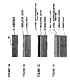
- a substrate 5 is prepared as shown in Figure 1A.
- This substrate 5 is formed of for example, an insulating substrate such as a MgO (100) substrate, a SrTi0 3 (100) substrate or others, or a semiconductor substrate such as a silicon (100) substrate having a principal surface coated with insulating films.
- an insulating substrate such as a MgO (100) substrate, a SrTi0 3 (100) substrate or others
- a semiconductor substrate such as a silicon (100) substrate having a principal surface coated with insulating films.
- a principal surface of the semiconductor substrate is continuously coated with MgA1 2 0 4 by a CVD process and with BaTi0 3 by a sputtering process.
- an insulating layer 7 such as a MgO and others is deposited on a principal surface or deposition surface 5A of the substrate 5 by a sputtering process, so as to have a thickness of about 200nm.
- the insulating layer 7 can be omitted.
- a c-axis oriented oxide superconductor thin film 11 which has a thickness of not greater than about 100nm and which will form a superconducting gate electrode, is deposited on the insulating layer 7, by for example an off-axis sputtering, a reactive evaporation, an MBE (molecular beam epitaxy), a CVD, etc.
- the oxide superconductor material is preferably formed of, for example, a Y-Ba-Cu-0 type compound oxide superconductor material, a Bi-Sr-Ca-Cu-O type compound oxide superconductor material, and a TI-Ba-Ca-Cu-O type compound oxide superconductor material.
- the c-axis orientated oxide superconductor thin film has a large critical current density in a direction parallel to the substrate.
- an insulating layer 8 such as a MgO and others is deposited on the principal surface of the oxide superconductor thin film 11 by a sputtering process, so as to have a thickness of about 300nm.
- the insulating layer 7, the oxide superconductor thin film 11 and the insulating layer 8 are continuously deposited without being taken out of a deposition chamber.
- an right portion (in the drawing) of a stacked structure of the insulating layer7, the oxide superconductor thin film 11 and the insulating layer 8 is completely removed by an etching process, so that the stacked structure has a vertical end surface 15 extending from an upper surface of the insulating layer 8 to a bottom surface of the insulating layer 7, and a right portion of the substrate 5 is exposed.
- the end surface 15 is perpendicular to the principal surface or deposition surface 5A of the substrate 5.
- This etching is performed by using a scan type etching such as a focused ion beam etching.
- a gate insulator layer 6 is formed to cover the vertical end surface 15, an upper surface of the insulating layer 8, and the exposed surface of the substrate 5.
- the gate insulator layer 6 is formed of, for example, MgO, Si a N 4 , etc., and has a thickness sufficient to prevent a tunnel current, for example, a thickness of not less than 10 nanometers.
- an a-axis orientated oxide superconductor thin film 1 is deposited on the gate insulator layer 6 by an off-axis sputtering at a temperature of not greater than 650°C.
- This oxide superconductor thin film 1 is formed of the same oxide superconductor material as that of the oxide superconductor thin film 11 and has a thickness of not greater than 5nm.
- a portion of the oxide superconductor thin film 1 deposited above the upper surface of the insulating layer 8 and the exposed surface of the substrate 5 has the a-axis perpendicular to the principal surface or deposition surface 5A of the substrate 5, a portion of the oxide superconductor thin film 1 deposited above the vertical end surface 15 has the a-axis in parallel to the vertical end surface and therefore has a large critical current density in a direction parallel to the vertical end surface 15.
- a left end portion (in the drawing) of the oxide superconductor thin film 1, the gate insulator layer 6 and the insulating layer 8 is removed by a reactive ion etching or an Ar ion milling, so that a left end portion 14 of the superconducting gate electrode 11 is exposed.
- a gate electrode 4, a source electrode 2 and a drain electrode 3 are formed on the exposed left end portion 14 of the superconducting gate electrode 11, and opposite end portions of the the oxide superconductor thin film 1, respectively.
- These electrodes are preferably formed of a refractory metal such as Ti, W, etc., or Au, or a silicide thereof, by any appropriate process such as a vacuum evaporation process.
- a passivation film can be formed to cover these electrodes. With this, the super-FET is completed.
- the limitation in the fine processing technique required for manufacturing the super-FET is relaxed. Accordingly, it is easy to manufacture the super-FET with good repeatability, and the manufactured super-FET has a stable performance.
- the first embodiment of the super-FET in accordance with the present invention includes the superconducting gate electrode 11 of the oxide superconductor material stacked on the insulating layer formed on the substrate 5.
- the gate electrode 4 is formed on the left portion of the superconducting gate electrode 11.
- the superconducting gate electrode 11 has a right portion having an upper surface coated with the insulating layer 8, so that the insulating layer 7, the superconducting gate electrode 11 and the insulating layer 8 from the stacked structure.
- the stacked structure of the insulating layer 7, the superconducting gate electrode 11 and the insulating layer 8 has a single common right end surface 15 perpendicularly to the principal surface or deposition surface 5A of the substrate 5.
- the gate insulator layer 6 and the oxide superconductor thin film 1 are formed in the named order, and the gate insulator layer 6 and the oxide superconductor thin film 1 extend continuously to extend on the upper surface of the insulating layer 8 and the upper surface of the substrate 5.
- This superconducting channel 10 has a large critical current density along a current flowing direction within the superconducting channel 10, since as mentioned above the portion of the oxide superconductor thin film 1 deposited above the vertical end surface 15 has the a-axis in parallel to the vertical end surface and therefore has a large critical current density in a direction parallel to the vertical end surface 15.
- the source electrode 2 and the drain electrode 3 are formed on opposite end portions of the oxide superconductor thin film 1.
- an right portion (in the drawing) of a stacked structure of the insulating layer 7, the oxide superconductor thin film 11 and the insulating layer 8 is removed by an etching process so as to have a common single inclined end surface 15, and a right portion of the substrate 5 is exposed.
- This etching is performed by using a scan type etching such as a focused ion beam etching.
- a gate insulator layer 6 is formed to cover the inclined end surface 15, an upper surface of the insulating layer 8, and the exposed surface of the substrate 5.
- the gate insulator layer 6 is formed of, for example, MgO, Si a N 4 , etc., and has a thickness sufficient to prevent a tunnel current, for example, a thickness of not less than 10 nanometers.
- a c-axis oriented oxide superconductor thin film 1 is deposited on the gate insulator layer 6 by an off-axis sputtering at a temperature of about 700°C.
- This oxide superconductor thin film 1 is formed of the same oxide superconductor material as that of the oxide superconductor thin film 11 and has a thickness of not greater than 5nm.
- a portion of the oxide superconductor thin film 1 deposited above the inclined end surface 15 has the c-axis perpendicular to the inclined end surface and therefore has a large critical current density in a direction parallel to the inclined end surface 15.
- a left end portion (in the drawing) of the oxide superconductor thin film 1, the gate insulator layer 6 and the insulating layer 8 is removed by a reactive ion etching or an Ar ion milling, so that a left end portion 14 of the superconducting gate electrode 11 is exposed.
- a gate electrode 4, a source electrode 2 and a drain electrode 3 are formed on the exposed left end portion 14 of the superconducting gate electrode 11, and opposite end portions of the the oxide superconductor thin film 1, respectively.
- These electrodes are preferably formed of refractory metal such as Ti, W, etc., or Au, or a silicide thereof, by any appropriate process such as a vacuum evaporation process.
- a passivation film can be formed to cover these electrodes. With this, the super-FET is completed.
- limitation in the fine processing technique required for manufacturing the super-FET is also relaxed. Accordingly, it is easy to manufacture the super-FET with good repeatability, and the manufactured super-FET has a stable performance.
- the second embodiment of the super-FET in accordance with the present invention includes the superconducting gate electrode 11 of the oxide superconductor material stacked on the insulating layer 7 formed on the substrate 5.
- the gate electrode 4 is formed on the left portion of the superconducting gate electrode 11.
- the superconducting gate electrode 11 has the right portion having an upper surface coated with the insulating layer 8 so that the insulating layer 7, the superconducting gate electrode 11 and the insulating layer 8 form the stacked structure.
- the stacked structure of the insulating layer 7, the superconducting gate electrode 11 and the insulating layer 8 has a single common end surface 15 inclined to the principal surface or deposition surface 5A of the substrate 5.
- the gate insulator layer 6 and the oxide superconductor thin film 1 are formed in the named or- derso as to continuously extend on the upper surface of the insulating layer 8 and the upper surface of the substrate 5.
- This superconducting channel 10 has a large critical current density along a current flowing direction within the superconducting channel 10, since as mentioned above the portion of the oxide superconductor thin film 1 deposited above the inclined end surface 15 has the c-axis perpendicular to the inclined end surface and therefore has a large critical current density in a direction parallel to the inclined end surface 15.
- the source electrode 2 and the drain electrode 3 are formed on the opposite end portions of the oxide superconductor thin film 1.
- the oxide superconductor thin film 11 forming the superconducting gate electrode is deposited to have a thickness of 50nm.
- the angle of the inclined end surface 15 to the deposition surface 5A of the substrate 5 and the thickness of the oxide superconductor thin film 11 constituting the gate electrode is determined on the basis of the gate length to be obtained.
- the superconducting device in accordance with the present invention a main current flows through the superconducting channel and is controlled by the gate voltage. Therefore, differently from the conventional super-FET in which a superconducting current flows through the semiconductor channel due to the superconducting proximity effect, the fine processing techniques which had been required for manufacturing the super-FET have become unnecessary. In addition, since it is not necessary to stack the superconductor and the semiconductor, high performance superconducting device can be realized by using an oxide superconductor. Furthermore, since the gate length can be shortened, the superconducting devise in accordance with the present invention can operate at a high speed. Therefore, the application of the superconduction technology to the electronic devices can be promoted.
Landscapes
- Superconductor Devices And Manufacturing Methods Thereof (AREA)
Description
- The present invention relates to a superconducting device and a method for manufacturing the same, and more specifically to a superconducting device including an extremely short superconducting channel formed of oxide superconductor material, and a method for manufacturing the same.
- Typical three-terminal devices which utilize a superconductor include a so called superconducting-base transistor and a so called super-FET (field effect transistor). The superconducting-base transistor includes an emitter of a superconductor or a normal conductor, a tunnel barrier of an insulator, a base of a superconductor, a semiconductor isolator and a collector of a normal conductor, stacked in the named order. This superconducting-base transistor operates at a high speed with a low power consumption, by utilizing high speed electrons passing through the tunnel barrier.
- The super-FET includes a semiconductor layer, and a superconductor source electrode and a superconductor drain electrode which are formed closely to each other on the semiconductor layer. A portion of the semiconductor layer between the superconductor source electrode and the superconductor drain electrode has a greatly recessed or undercut war surface so as to have a reduced thickness. In addition, a gate electrode is formed through a gate insulating layer on the recessed or undercut rear surface of the portion of the semiconductor layer between the superconductor source electrode and the superconductor drain electrode.
- In the above mentioned super-FET, a superconducting current flows through the semiconductor layer portion between the superconductor source electrode and the superconductor drain electrode due to a proximity effect, and is controlled by an applied gate voltage. This super-FET also operates at a high speed with a low power consumption, (see for example IBM Technical Disclosure Bulletin, Vol. 32, No 3A, August 1989, pp. 77-78).
- In addition, in the prior art, there has been proposed a three-terminal superconducting device having a channel of a superconductor formed between a source electrode and a drain electrode, so that a current flowing through the superconducting channel is controlled by a voltage applied to a gate formed above the superconducting channel.
- Both of the above mentioned superconducting-base transistor and the super-FET have a portion in which a semiconductor layer and a superconducting layer are stacked to each other. However, it is difficult to form a stacked structure of the semiconductor layer and the superconducting layer formed of an oxide superconductor which has been recently advanced in study. In addition, even if it is possible to form a stacked structure of the semiconductor layer and the oxide superconducting layer, it is difficult to control a boundary between the semiconductor layer and the oxide superconducting layer. Therefore, a satisfactory operation could not been obtained in these superconducting devices.
- In addition, since the super-FET utilizes the proximity effect, the superconductor source electrode and the superconductor drain electrode have to be located close to each other at a distance which is not greater than a few times the coherence length of the superconductor materials of the superconductor source electrode and the superconductor drain electrode. In particular, since the oxide superconductor has a short coherence length, if the superconductor source electrode and the superconductor drain electrode are formed of the oxide superconductor material, a distance between the superconductor source electrode and the superconductor drain electrode has to be not greater than a few ten nanometers. However, it is very difficult to conduct a fine processing such as a fine pattern etching so as to ensure the very short separation distance. Because of this, in the prior art, it has been impossible to manufacture the super-FET composed of the oxide superconductor material.
- Furthermore, it has been confirmed that the conventional three-terminal superconducting device having the superconducting channel shows a modulation operation. However, the conventional three-terminal superconducting device having the superconducting channel could not realize a complete ON/OFF operation, because a carrier density is too high. In this correction, since an oxide superconductor material has a low carrier density, it is expected to form a three-terminal superconducting device which has a superconducting channel and which can realize the complete ON/OFF operation, by forming the superconducting channel of the oxide superconductor material. In this case, however, a thickness of the superconducting channel has to be made on the order of five nanometers or less.
- Furthermore, the operation speed of this device is determined by a gate length. However, it is difficult to realize this dimension of not greater than 0.1 f..lm by use of the conventional processing technique, and therefore, there has been a limit in speeding up the operation speed of the device.
- Accordingly, it is an object of the present invention to provide a superconducting device and a method for manufacturing the same, which have overcome the above mentioned defects of the conventional ones.
- Another object of the present invention is to provide a superconducting device including a superconducting region constituted of an extremely thin oxide superconductor film, which can be manufactured by using existing established processing techniques with a good repeatability.
- Still another object of the present invention is to provide an FET type superconducting device including an extremely short superconducting channel composed of an oxide superconductor thin film, and a method for manufacturing the same with a good repeatability by using existing established processing techniques.
- The above and other objects of the present invention are achieved in accordance with the present invention by a superconducting device comprising a substrate, a superconducting channel constituted of an oxide superconductor thin film formed to have an angle to a deposition surface of the substrate, a superconductor source electrode and a superconductor drain electrode formed at opposite ends of the superconducting channel, so that a superconducting current can flow through the superconducting channel between the superconductor source electrode and the superconductor drain electrode, and a gate electrode in the form of a sheet having an end abutted through an insulating layer on the superconducting channel so as to control the superconducting current flowing through the superconducting channel, the gate electrode being formed of an oxide superconductor thin film in parallel to the deposition surface of the substrate.
- Here, the source electrode should be understood to include not only an electrode corresponding to the electrode which is called a "source electrode" in the field of a semiconductor MOSFET, but also a source region which is formed adjacent to and continuous to the superconducting channel and on which the source electrode is formed, and the drain electrode should be understood to include not only an electrode corresponding to the electrode which is called a "drain electrode" in the field of the semiconductor MOSFET, but also a drain region which is formed adjacent to and continuous to the superconducting channel and on which the drain electrode is formed.
- In addition, the angle of the oxide superconductor thin film of the superconducting channel to the deposition surface of the substrate is determined, in the range of greater than 0° but less than 180°, on the basis of the thickness of the oxide superconductor thin film constituting the gate electrode and the gate length to be obtained. In practice, this angle is preferably not less than 30° but not greater than 90°. Therefore, this angle should be 90° in order to obtain the shortest gate length in a given thickness of the oxide superconductor thin film constituting the gate electrode. However, even if the angle is selected in the range of not less than 30° but not greater than 90°, a desired gate length can be obtained by controlling the thickness of the oxide superconductor thin film constituting the gate electrode.
- As seen from the above, the superconducting device in accordance with the present invention is characterized in that the superconducting channel is constituted of the oxide superconductor thin film and formed to have some angle to the deposition surface of the substrate, and in that the gate electrode is formed of the oxide superconductor thin film in parallel to the deposition surface of the deposition surface of the substrate, so that an end of the oxide superconductor thin film of the gate electrode is in contact with the gate insulator so as to oppose through the insulating layer to the superconducting channel. The oxide superconductor thin film of the gate electrode can be formed to have a thickness of not greater than about 100nm. Therefore, a gate length of the gate electrode is substantially determined by the thickness of the oxide superconductor thin film of the gate electrode. In the super-FET, since the channel length is substantially determined by the gate length of the gate electrode, the super-FET in accordance with the present invention can have an extremely short superconducting channel which is controlled by the gate electrode, and accordingly, the current flowing through the superconducting channel can be turned on and off at a high speed. In addition, the superconducting device in accordance with the present invention can have the above mentioned shortened gate without using the fine-processing technique.
- In order to ensure that the superconducting channel can be turned on and off by a voltage applied to the gate electrode, a thickness of the superconducting channel has to be not greater than five nanometers in the direction of an electric field created by the voltage applied to the gate electrode. This extremely thin superconducting channel is realized in the superconducting device in accordance with the present invention.
- Furthermore, differently film the conventional super-FET in which a superconducting current flows through the semiconductor channel due to the superconducting proximity effect, the superconducting device in accordance with the present invention is constructed so that a main current flows through the superconductor material. Therefore, the superconducting device in accordance with the present invention is not required to locate the pair of superconducting electrodes apart from each other by an extremely short distance. In addition, in the superconducting device in accordance with the present invention, the shortened gate can be formed without using the fine-processing technique as mentioned above, and the superconducting channel can be also formed without using the fine-processing technique as will be explained hereinafter. Therefore, the limitation in the fine processing techniques required for manufacturing the super-FET can be relaxed.
- The above mentioned superconducting device in accordance with the present invention can be formed by the method in accordance with the present invention for manufacturing the superconducting device, which method includes the step of forming and stacking a first oxide superconducting thin film and a first insulating layer on an insulating surface of a substrate in the name order, partially removing the stacked structure of the first oxide superconducting thin film and the first insulating layer so as to have a smooth continuous end surface having an angle to the insulating surface of a substrate and extending from the first insulating layer at least to a bottom surface of the first oxide superconducting thin film, and forming and stacking a second insulating layer and a second oxide superconducting thin film in the name order on the end surface of the stacked structure of the first oxide superconducting thin film and the first insulating layer, so that the first oxide superconducting thin film functions as a gate electrode and the second insulating layer functions as a gate insulator and so that a first portion of the second oxide superconducting thin film joining to the end surface of the first oxide superconducting thin film through the second insulating layer forms a superconducting channel, and second and third portions of the second oxide superconducting thin film at both sides of the first portion of the second oxide superconducting thin film form a source and a drain, respectively.
- As seen from the above, in the method of the present invention, the first oxide superconducting thin film constituting the superconducting gate electrode is first formed on the substrate. In this connection, a film of an insulator such as MgO can be formed on the substrate if necessary, and thereafter, the first oxide superconducting thin film can be formed on the insulator film.
- Then, the first insulating layer is deposited on the first oxide superconducting thin film, and the stacked structure of the first oxide superconducting thin film and the first insulating layer is partially etched to have a smooth continuous end surface having an angle to the deposition surface of the substrate and extending from the first insulating layer at least to a bottom surface of the first oxide superconducting thin film. This etching can be performed by using, preferably, a scan type etching such as a focused ion beam etching. Thereafter, a second insulating layer constituting the gate insulator and the second oxide superconductor thin film constituting the superconducting channel are formed on the end surface of the stacked structure of the first oxide superconducting thin film and the first insulating layer.
- The oxide superconductor thin film constituting the superconducting channel has to have a thickness on the order of about five nanometers or less. Such an extremely thin oxide superconductor thin film can be formed in a conventional process by precisely controlling the growth speed and the growth time of the thin film. For this purpose, a sputtering can be used. However, since the oxide superconductor crystal has a multi-layer structure in which respective constituent elements are stacked in a layered structure, it is possible to stack a desired number of units cells of oxide superconductor, by using a MBE (molecular beam epitaxy).
- In the method in accordance with the present invention for manufacturing the superconducting device, there is neither a fine-etching nor a fine-patterning of the superconducting thin film. Therefore, it is possible to relax the limitation in the fine processing techniques such as a fine-etching or a fine-patterning which has been required in the case that conventional super-FET is formed of an oxide superconductor material. In addition, the stacked structure of the oxide superconducting layer and the semiconductor layer is no longer necessary.
- In a preferred embodiment of the superconducting device in accordance with the present invention, the oxide superconductor thin films is formed of a high-Tc (high critical temperature) oxide superconductor material. This high-Tc oxide superconductor material has been studied by many researchers since the discovery of Bednorz and Muller in 1986, and is said to indicate an oxide superconductor material having a critical temperature of not less than 30K. More specifically, the oxide superconductor thin film is formed of a high-Tc copper-oxide type oxide superconductor material including a Y-Ba-Cu-0 type compound oxide superconductor material, a Bi-Sr-Ca-Cu-O type compound oxide superconductor material, and a TI-Ba-Ca-Cu-O the compound oxide superconductor material.
- In addition, the substrate, on which the oxide superconductor thin film is deposited, can be formed of an insulating substrate, preferably an oxide single crystalline substrate such as MgO, SrTi03, and CdNdAI04. These substrate materials are very effective in forming or growing a crystalline film having a high orientation property. However, the superconducting device can be formed on a semiconductor substrate if an appropriate buffer layer is deposited thereon. For example, the buffer layer on the semiconductor substrate can be formed of a double-layer coating formed of a MgA1204 layer and a BaTi03 layer if a silicon substrate is used.
- The above and other objects, features and advantages of the present invention will be apparent from the following description of preferred embodiments of the invention with reference to the accompanying drawings.
-
- Figures 1Ato 11 are diagrammatic sectional views for illustrating a first embodiment of the process in accordance with the present invention for manufacturing the super-FET; and
- Figures 2Ato 21 are diagrammatic sectional views for illustrating a second embodiment of the process in accordance with the present invention for manufacturing the super-FET.
- Referring to Figures 1A to 11, a first embodiment of the process in accordance with the present invention for manufacturing the super-FET will be described.
- First, a
substrate 5 is prepared as shown in Figure 1A. Thissubstrate 5 is formed of for example, an insulating substrate such as a MgO (100) substrate, a SrTi03 (100) substrate or others, or a semiconductor substrate such as a silicon (100) substrate having a principal surface coated with insulating films. However, if the semiconductor substrate is used, a principal surface of the semiconductor substrate is continuously coated with MgA1204 by a CVD process and with BaTi03 by a sputtering process. - Then, as shown in Figure 1 B, an insulating
layer 7 such as a MgO and others is deposited on a principal surface ordeposition surface 5A of thesubstrate 5 by a sputtering process, so as to have a thickness of about 200nm. However, if the substrate has good insulation property and good crystallinity, the insulatinglayer 7 can be omitted. - Then, as shown in Figure 1C, a c-axis oriented oxide superconductor
thin film 11, which has a thickness of not greater than about 100nm and which will form a superconducting gate electrode, is deposited on the insulatinglayer 7, by for example an off-axis sputtering, a reactive evaporation, an MBE (molecular beam epitaxy), a CVD, etc. The oxide superconductor material is preferably formed of, for example, a Y-Ba-Cu-0 type compound oxide superconductor material, a Bi-Sr-Ca-Cu-O type compound oxide superconductor material, and a TI-Ba-Ca-Cu-O type compound oxide superconductor material. The c-axis orientated oxide superconductor thin film has a large critical current density in a direction parallel to the substrate. - As shown in Figure 2D, an insulating
layer 8 such as a MgO and others is deposited on the principal surface of the oxide superconductorthin film 11 by a sputtering process, so as to have a thickness of about 300nm. In order to reduce a mechanical stress, it is preferred that the insulatinglayer 7, the oxide superconductorthin film 11 and the insulatinglayer 8 are continuously deposited without being taken out of a deposition chamber. - Thereafter, as shown in Figure 1 E, an right portion (in the drawing) of a stacked structure of the insulating layer7, the oxide superconductor
thin film 11 and the insulatinglayer 8 is completely removed by an etching process, so that the stacked structure has avertical end surface 15 extending from an upper surface of the insulatinglayer 8 to a bottom surface of the insulatinglayer 7, and a right portion of thesubstrate 5 is exposed. Theend surface 15 is perpendicular to the principal surface ordeposition surface 5A of thesubstrate 5. This etching is performed by using a scan type etching such as a focused ion beam etching. - As shown in Figure 1 F, a
gate insulator layer 6 is formed to cover thevertical end surface 15, an upper surface of the insulatinglayer 8, and the exposed surface of thesubstrate 5. Thegate insulator layer 6 is formed of, for example, MgO, SiaN4, etc., and has a thickness sufficient to prevent a tunnel current, for example, a thickness of not less than 10 nanometers. - As shown in Figure 1 G, an a-axis orientated oxide superconductor
thin film 1 is deposited on thegate insulator layer 6 by an off-axis sputtering at a temperature of not greater than 650°C. This oxide superconductorthin film 1 is formed of the same oxide superconductor material as that of the oxide superconductorthin film 11 and has a thickness of not greater than 5nm. Therefore, since a portion of the oxide superconductorthin film 1 deposited above the upper surface of the insulatinglayer 8 and the exposed surface of thesubstrate 5 has the a-axis perpendicular to the principal surface ordeposition surface 5A of thesubstrate 5, a portion of the oxide superconductorthin film 1 deposited above thevertical end surface 15 has the a-axis in parallel to the vertical end surface and therefore has a large critical current density in a direction parallel to thevertical end surface 15. - As shown in Figure 1 H, a left end portion (in the drawing) of the oxide superconductor
thin film 1, thegate insulator layer 6 and the insulatinglayer 8 is removed by a reactive ion etching or an Ar ion milling, so that aleft end portion 14 of thesuperconducting gate electrode 11 is exposed. - Thereafter, as shown in Figure 11, a gate electrode 4, a
source electrode 2 and adrain electrode 3 are formed on the exposedleft end portion 14 of thesuperconducting gate electrode 11, and opposite end portions of the the oxide superconductorthin film 1, respectively. These electrodes are preferably formed of a refractory metal such as Ti, W, etc., or Au, or a silicide thereof, by any appropriate process such as a vacuum evaporation process. In addition, if necessary, a passivation film can be formed to cover these electrodes. With this, the super-FET is completed. - According to the first embodiment of the method of the present invention, the limitation in the fine processing technique required for manufacturing the super-FET is relaxed. Accordingly, it is easy to manufacture the super-FET with good repeatability, and the manufactured super-FET has a stable performance.
- As seen from the above description and shown in Figure 11, the first embodiment of the super-FET in accordance with the present invention includes the
superconducting gate electrode 11 of the oxide superconductor material stacked on the insulating layer formed on thesubstrate 5. The gate electrode 4 is formed on the left portion of thesuperconducting gate electrode 11. On the other hand, thesuperconducting gate electrode 11 has a right portion having an upper surface coated with the insulatinglayer 8, so that the insulatinglayer 7, thesuperconducting gate electrode 11 and the insulatinglayer 8 from the stacked structure. - The stacked structure of the insulating
layer 7, thesuperconducting gate electrode 11 and the insulatinglayer 8 has a single commonright end surface 15 perpendicularly to the principal surface ordeposition surface 5A of thesubstrate 5. On the perpendicularright end surface 15, thegate insulator layer 6 and the oxide superconductorthin film 1 are formed in the named order, and thegate insulator layer 6 and the oxide superconductorthin film 1 extend continuously to extend on the upper surface of the insulatinglayer 8 and the upper surface of thesubstrate 5. - With this arrangement, a portion of the oxide superconductor
thin film 1 positioned just in front of the end of thesuperconducting gate electrode 11, forms asuperconducting channel 10. Thissuperconducting channel 10 has a large critical current density along a current flowing direction within thesuperconducting channel 10, since as mentioned above the portion of the oxide superconductorthin film 1 deposited above thevertical end surface 15 has the a-axis in parallel to the vertical end surface and therefore has a large critical current density in a direction parallel to thevertical end surface 15. Thesource electrode 2 and thedrain electrode 3 are formed on opposite end portions of the oxide superconductorthin film 1. - Referring to Figures 2A to 21, a second embodiment of the process in accordance with the present invention for manufacturing the super-FET will be described. In Figures 2A to 21, the elements similar or corresponding to those shown in Figures 1A to 11 are given the same References Numerals, and only portions or steps different from those of the first embodiments will be explained.
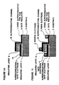
- The same processes as those shown in Figures 1 A to 1D are performed in steps shown in Figure 2A to 2D.
- The process shown in Figure 2E is different from that shown in Figure 1 E, only in that an
inclined end surface 15 is formed in the process shown in Figure 2E, in place of the vertical end surface shown in Figure 1 E. - Namely, as shown in Figure 2E, an right portion (in the drawing) of a stacked structure of the insulating
layer 7, the oxide superconductorthin film 11 and the insulatinglayer 8 is removed by an etching process so as to have a common singleinclined end surface 15, and a right portion of thesubstrate 5 is exposed. This etching is performed by using a scan type etching such as a focused ion beam etching. - As shown in Figure 2F, a
gate insulator layer 6 is formed to cover theinclined end surface 15, an upper surface of the insulatinglayer 8, and the exposed surface of thesubstrate 5. Thegate insulator layer 6 is formed of, for example, MgO, SiaN4, etc., and has a thickness sufficient to prevent a tunnel current, for example, a thickness of not less than 10 nanometers. - As shown in Figure 2G, a c-axis oriented oxide superconductor
thin film 1 is deposited on thegate insulator layer 6 by an off-axis sputtering at a temperature of about 700°C. This oxide superconductorthin film 1 is formed of the same oxide superconductor material as that of the oxide superconductorthin film 11 and has a thickness of not greater than 5nm. A portion of the oxide superconductorthin film 1 deposited above theinclined end surface 15 has the c-axis perpendicular to the inclined end surface and therefore has a large critical current density in a direction parallel to theinclined end surface 15. - As shown in Figure 2H, a left end portion (in the drawing) of the oxide superconductor
thin film 1, thegate insulator layer 6 and the insulatinglayer 8 is removed by a reactive ion etching or an Ar ion milling, so that aleft end portion 14 of thesuperconducting gate electrode 11 is exposed. - Thereafter, as shown in Figure 21, a gate electrode 4, a
source electrode 2 and adrain electrode 3 are formed on the exposedleft end portion 14 of thesuperconducting gate electrode 11, and opposite end portions of the the oxide superconductorthin film 1, respectively. These electrodes are preferably formed of refractory metal such as Ti, W, etc., or Au, or a silicide thereof, by any appropriate process such as a vacuum evaporation process. In addition, if necessary, a passivation film can be formed to cover these electrodes. With this, the super-FET is completed. - According to the second embodiment of the method of the present invention, limitation in the fine processing technique required for manufacturing the super-FET is also relaxed. Accordingly, it is easy to manufacture the super-FET with good repeatability, and the manufactured super-FET has a stable performance.
- As seen from the above description and shown in Figure 21, the second embodiment of the super-FET in accordance with the present invention includes the
superconducting gate electrode 11 of the oxide superconductor material stacked on the insulatinglayer 7 formed on thesubstrate 5. The gate electrode 4 is formed on the left portion of thesuperconducting gate electrode 11. On the other hand, thesuperconducting gate electrode 11 has the right portion having an upper surface coated with the insulatinglayer 8 so that the insulatinglayer 7, thesuperconducting gate electrode 11 and the insulatinglayer 8 form the stacked structure. - The stacked structure of the insulating
layer 7, thesuperconducting gate electrode 11 and the insulatinglayer 8 has a singlecommon end surface 15 inclined to the principal surface ordeposition surface 5A of thesubstrate 5. On the inclinedright end surface 15, thegate insulator layer 6 and the oxide superconductorthin film 1 are formed in the named or- derso as to continuously extend on the upper surface of the insulatinglayer 8 and the upper surface of thesubstrate 5. - With this arrangement, a portion of the oxide superconductor
thin film 1 positioned just in front of the end of thesuperconducting gate electrode 11, forms asuperconducting channel 10. Thissuperconducting channel 10 has a large critical current density along a current flowing direction within thesuperconducting channel 10, since as mentioned above the portion of the oxide superconductorthin film 1 deposited above theinclined end surface 15 has the c-axis perpendicular to the inclined end surface and therefore has a large critical current density in a direction parallel to theinclined end surface 15. Thesource electrode 2 and thedrain electrode 3 are formed on the opposite end portions of the oxide superconductorthin film 1. - In addition, in order to obtain a gate length of 100nm in the second embodiment, if the
inclined end surface 15 has an angle of 30° to the deposition surface of thesubstrate 5, the oxide superconductorthin film 11 forming the superconducting gate electrode is deposited to have a thickness of 50nm. Similarly, the angle of theinclined end surface 15 to thedeposition surface 5A of thesubstrate 5 and the thickness of the oxide superconductorthin film 11 constituting the gate electrode is determined on the basis of the gate length to be obtained. - As explained above, in the superconducting device in accordance with the present invention, a main current flows through the superconducting channel and is controlled by the gate voltage. Therefore, differently from the conventional super-FET in which a superconducting current flows through the semiconductor channel due to the superconducting proximity effect, the fine processing techniques which had been required for manufacturing the super-FET have become unnecessary. In addition, since it is not necessary to stack the superconductor and the semiconductor, high performance superconducting device can be realized by using an oxide superconductor. Furthermore, since the gate length can be shortened, the superconducting devise in accordance with the present invention can operate at a high speed. Therefore, the application of the superconduction technology to the electronic devices can be promoted.
- The invention has thus been shown and described with reference to the specific embodiments. However, it should be noted that the present invention is in no way limited to the details of the illustrated structures but changes and modifications may be made within the scope of the appended claims.
Claims (14)
Applications Claiming Priority (6)
| Application Number | Priority Date | Filing Date | Title |
|---|---|---|---|
| JP291197/90 | 1990-10-29 | ||
| JP2291198A JP2614940B2 (en) | 1990-10-29 | 1990-10-29 | Superconducting element and fabrication method |
| JP29119790 | 1990-10-29 | ||
| JP29119890 | 1990-10-29 | ||
| JP291198/90 | 1990-10-29 | ||
| JP2291197A JP2614939B2 (en) | 1990-10-29 | 1990-10-29 | Superconducting element and fabrication method |
Publications (4)
| Publication Number | Publication Date |
|---|---|
| EP0484232A2 EP0484232A2 (en) | 1992-05-06 |
| EP0484232A3 EP0484232A3 (en) | 1992-08-12 |
| EP0484232B1 true EP0484232B1 (en) | 1995-04-19 |
| EP0484232B2 EP0484232B2 (en) | 2001-10-10 |
Family
ID=26558442
Family Applications (1)
| Application Number | Title | Priority Date | Filing Date |
|---|---|---|---|
| EP91402900A Expired - Lifetime EP0484232B2 (en) | 1990-10-29 | 1991-10-29 | Superconducting device having an extremely short superconducting channel formed of oxide superconductor material and method for manufacturing the same |
Country Status (4)
| Country | Link |
|---|---|
| US (1) | US5854493A (en) |
| EP (1) | EP0484232B2 (en) |
| CA (1) | CA2054477C (en) |
| DE (1) | DE69109054T3 (en) |
Families Citing this family (7)
| Publication number | Priority date | Publication date | Assignee | Title |
|---|---|---|---|---|
| DE69118106T2 (en) * | 1990-10-31 | 1996-10-31 | Sumitomo Electric Industries | Superconducting device formed from extremely thin superconducting oxide film with an extremely short channel and method for its production |
| KR0148596B1 (en) * | 1994-11-28 | 1998-10-15 | 양승택 | Superconducting field effect element with grain boundary channel and its manufacturing method |
| KR0175359B1 (en) * | 1995-12-15 | 1999-02-01 | 양승택 | Method for fabricating superconductor-insulator-superconductor josephson tunnel junction structure |
| JP2002266072A (en) * | 2001-03-09 | 2002-09-18 | Sumitomo Electric Ind Ltd | Laminated film and film forming method |
| US20070254402A1 (en) * | 2006-04-27 | 2007-11-01 | Robert Rotzoll | Structure and fabrication of self-aligned high-performance organic fets |
| US10367134B2 (en) * | 2017-06-07 | 2019-07-30 | International Business Machines Corporation | Shadow mask sidewall tunnel junction for quantum computing |
| FR3068518B1 (en) * | 2017-06-28 | 2019-08-30 | Commissariat A L'energie Atomique Et Aux Energies Alternatives | METHOD FOR CONTROLLING A QUANTUM DEVICE WITH A QUANTITY OF SPIN |
Family Cites Families (6)
| Publication number | Priority date | Publication date | Assignee | Title |
|---|---|---|---|---|
| JPS6117983A (en) * | 1984-07-04 | 1986-01-25 | 日本原子力事業株式会社 | Emergency stop device for nuclear reactor |
| US4831421A (en) * | 1985-10-11 | 1989-05-16 | International Business Machines Corporation | Superconducting device |
| US5179426A (en) * | 1987-08-04 | 1993-01-12 | Seiko Epson Corporation | Josephson device |
| DE3876228T2 (en) * | 1988-01-15 | 1993-06-03 | Ibm | FIELD EFFECT ARRANGEMENT WITH SUPRAL-CONDUCTING CHANNEL. |
| JPH01268075A (en) * | 1988-04-19 | 1989-10-25 | Seiko Epson Corp | Josephson field-effect transistor |
| JPH01308086A (en) * | 1988-06-07 | 1989-12-12 | Fujitsu Ltd | Solid-state electronic device |
-
1991
- 1991-10-29 CA CA002054477A patent/CA2054477C/en not_active Expired - Fee Related
- 1991-10-29 EP EP91402900A patent/EP0484232B2/en not_active Expired - Lifetime
- 1991-10-29 DE DE69109054T patent/DE69109054T3/en not_active Expired - Lifetime
-
1997
- 1997-04-14 US US08/843,297 patent/US5854493A/en not_active Expired - Fee Related
Also Published As
| Publication number | Publication date |
|---|---|
| CA2054477A1 (en) | 1992-04-30 |
| CA2054477C (en) | 1996-12-24 |
| EP0484232A3 (en) | 1992-08-12 |
| DE69109054T2 (en) | 1995-11-30 |
| EP0484232A2 (en) | 1992-05-06 |
| DE69109054D1 (en) | 1995-05-24 |
| DE69109054T3 (en) | 2002-05-02 |
| EP0484232B2 (en) | 2001-10-10 |
| US5854493A (en) | 1998-12-29 |
Similar Documents
| Publication | Publication Date | Title |
|---|---|---|
| EP0480814B1 (en) | Superconducting device having an extremely thin superconducting channel formed of oxide superconductor material and method for manufacturing the same | |
| US5407903A (en) | Superconducting device having a reduced thickness of oxide superconducting layer | |
| EP0533568A1 (en) | Superconducting thin film formed of oxide superconductor material, superconducting device utilizing the superconducting thin film and method for manufacturing thereof | |
| EP0484253B1 (en) | Superconducting device having an extremely thin superconducting channel formed of oxide superconductor material and method for manufacturing the same | |
| EP0545801B1 (en) | Superconducting device having an extremely thin superconducting channel formed of oxide superconductor material and method for manufacturing the same | |
| EP0484232B1 (en) | Superconducting device having an extremely short superconducting channel formed of oxide superconductor material and method for manufacturing the same | |
| EP0477103B1 (en) | Method for manufacturing superconducting device having a reduced thickness of oxide superconducting layer and superconducting device manufactured thereby | |
| US5621223A (en) | Superconducting device having a reduced thickness of oxide superconducting layer and method for manufacturing the same | |
| EP0477063B1 (en) | Superconducting device having a reduced thickness of oxide superconducting layer and method for manufacturing the same | |
| US5714767A (en) | Method for manufacturing superconducting device having a reduced thickness of oxide superconducting layer and superconducting device manufactured thereby | |
| EP0551033B1 (en) | Superconducting device having an extremely thin superconducting channel formed of oxide superconductor material and method for manufacturing the same | |
| EP0533519B1 (en) | Superconducting device having an extremely thin superconducting channel formed of oxide superconductor material and method for manufacturing the same | |
| EP0478463B1 (en) | Superconducting device having an extremely thin superconducting channel formed of oxide superconductor material | |
| JP2614939B2 (en) | Superconducting element and fabrication method | |
| JP2614940B2 (en) | Superconducting element and fabrication method | |
| JP2641976B2 (en) | Superconducting element and fabrication method | |
| EP0790655B1 (en) | Superconducting field effect device having a superconducting channel and method for manufacturing the same | |
| JP2597743B2 (en) | Superconducting element fabrication method | |
| US5770470A (en) | High temperature superconducting electric field effect device and a method for fabricating the same | |
| JP2738144B2 (en) | Superconducting element and fabrication method |
Legal Events
| Date | Code | Title | Description |
|---|---|---|---|
| PUAI | Public reference made under article 153(3) epc to a published international application that has entered the european phase |
Free format text: ORIGINAL CODE: 0009012 |
|
| AK | Designated contracting states |
Kind code of ref document: A2 Designated state(s): DE FR GB |
|
| PUAL | Search report despatched |
Free format text: ORIGINAL CODE: 0009013 |
|
| AK | Designated contracting states |
Kind code of ref document: A3 Designated state(s): DE FR GB |
|
| 17P | Request for examination filed |
Effective date: 19920824 |
|
| 17Q | First examination report despatched |
Effective date: 19940829 |
|
| GRAA | (expected) grant |
Free format text: ORIGINAL CODE: 0009210 |
|
| AK | Designated contracting states |
Kind code of ref document: B1 Designated state(s): DE FR GB |
|
| REF | Corresponds to: |
Ref document number: 69109054 Country of ref document: DE Date of ref document: 19950524 |
|
| ET | Fr: translation filed | ||
| PLBI | Opposition filed |
Free format text: ORIGINAL CODE: 0009260 |
|
| 26 | Opposition filed |
Opponent name: SIEMENS AG Effective date: 19951213 |
|
| PLBF | Reply of patent proprietor to notice(s) of opposition |
Free format text: ORIGINAL CODE: EPIDOS OBSO |
|
| PLBF | Reply of patent proprietor to notice(s) of opposition |
Free format text: ORIGINAL CODE: EPIDOS OBSO |
|
| PLBO | Opposition rejected |
Free format text: ORIGINAL CODE: EPIDOS REJO |
|
| APAC | Appeal dossier modified |
Free format text: ORIGINAL CODE: EPIDOS NOAPO |
|
| APAE | Appeal reference modified |
Free format text: ORIGINAL CODE: EPIDOS REFNO |
|
| APAC | Appeal dossier modified |
Free format text: ORIGINAL CODE: EPIDOS NOAPO |
|
| APAE | Appeal reference modified |
Free format text: ORIGINAL CODE: EPIDOS REFNO |
|
| APAC | Appeal dossier modified |
Free format text: ORIGINAL CODE: EPIDOS NOAPO |
|
| PLAW | Interlocutory decision in opposition |
Free format text: ORIGINAL CODE: EPIDOS IDOP |
|
| PUAH | Patent maintained in amended form |
Free format text: ORIGINAL CODE: 0009272 |
|
| STAA | Information on the status of an ep patent application or granted ep patent |
Free format text: STATUS: PATENT MAINTAINED AS AMENDED |
|
| 27A | Patent maintained in amended form |
Effective date: 20011010 |
|
| AK | Designated contracting states |
Kind code of ref document: B2 Designated state(s): DE FR GB |
|
| REG | Reference to a national code |
Ref country code: GB Ref legal event code: IF02 |
|
| ET3 | Fr: translation filed ** decision concerning opposition | ||
| APAH | Appeal reference modified |
Free format text: ORIGINAL CODE: EPIDOSCREFNO |
|
| PGFP | Annual fee paid to national office [announced via postgrant information from national office to epo] |
Ref country code: DE Payment date: 20091022 Year of fee payment: 19 |
|
| PGFP | Annual fee paid to national office [announced via postgrant information from national office to epo] |
Ref country code: FR Payment date: 20091029 Year of fee payment: 19 Ref country code: GB Payment date: 20091028 Year of fee payment: 19 |
|
| GBPC | Gb: european patent ceased through non-payment of renewal fee |
Effective date: 20101029 |
|
| PG25 | Lapsed in a contracting state [announced via postgrant information from national office to epo] |
Ref country code: FR Free format text: LAPSE BECAUSE OF NON-PAYMENT OF DUE FEES Effective date: 20101102 |
|
| REG | Reference to a national code |
Ref country code: FR Ref legal event code: ST Effective date: 20110630 |
|
| PG25 | Lapsed in a contracting state [announced via postgrant information from national office to epo] |
Ref country code: GB Free format text: LAPSE BECAUSE OF NON-PAYMENT OF DUE FEES Effective date: 20101029 |
|
| REG | Reference to a national code |
Ref country code: DE Ref legal event code: R119 Ref document number: 69109054 Country of ref document: DE Effective date: 20110502 |
|
| PG25 | Lapsed in a contracting state [announced via postgrant information from national office to epo] |
Ref country code: DE Free format text: LAPSE BECAUSE OF NON-PAYMENT OF DUE FEES Effective date: 20110502 |