EP0420749A2 - Optical semiconductor device - Google Patents
Optical semiconductor device Download PDFInfo
- Publication number
- EP0420749A2 EP0420749A2 EP90402653A EP90402653A EP0420749A2 EP 0420749 A2 EP0420749 A2 EP 0420749A2 EP 90402653 A EP90402653 A EP 90402653A EP 90402653 A EP90402653 A EP 90402653A EP 0420749 A2 EP0420749 A2 EP 0420749A2
- Authority
- EP
- European Patent Office
- Prior art keywords
- layer
- well layer
- semiconductor device
- optical
- well
- Prior art date
- Legal status (The legal status is an assumption and is not a legal conclusion. Google has not performed a legal analysis and makes no representation as to the accuracy of the status listed.)
- Granted
Links
- 230000003287 optical effect Effects 0.000 title claims abstract description 109
- 239000004065 semiconductor Substances 0.000 title claims description 36
- 239000000203 mixture Substances 0.000 claims abstract description 25
- 238000010521 absorption reaction Methods 0.000 claims description 88
- 230000004888 barrier function Effects 0.000 claims description 43
- 229910000530 Gallium indium arsenide Inorganic materials 0.000 claims description 10
- KXNLCSXBJCPWGL-UHFFFAOYSA-N [Ga].[As].[In] Chemical compound [Ga].[As].[In] KXNLCSXBJCPWGL-UHFFFAOYSA-N 0.000 claims 8
- GPXJNWSHGFTCBW-UHFFFAOYSA-N Indium phosphide Chemical compound [In]#P GPXJNWSHGFTCBW-UHFFFAOYSA-N 0.000 claims 6
- AUCDRFABNLOFRE-UHFFFAOYSA-N alumane;indium Chemical compound [AlH3].[In] AUCDRFABNLOFRE-UHFFFAOYSA-N 0.000 claims 2
- 238000000862 absorption spectrum Methods 0.000 description 14
- 230000005684 electric field Effects 0.000 description 9
- 238000003475 lamination Methods 0.000 description 6
- 239000013078 crystal Substances 0.000 description 5
- 238000010586 diagram Methods 0.000 description 4
- 239000000463 material Substances 0.000 description 4
- 150000001875 compounds Chemical class 0.000 description 3
- 230000003247 decreasing effect Effects 0.000 description 2
- 230000000694 effects Effects 0.000 description 2
- 238000004519 manufacturing process Methods 0.000 description 2
- 238000005259 measurement Methods 0.000 description 2
- 238000001228 spectrum Methods 0.000 description 2
- 230000005540 biological transmission Effects 0.000 description 1
- 238000004364 calculation method Methods 0.000 description 1
- 238000005516 engineering process Methods 0.000 description 1
- 230000003993 interaction Effects 0.000 description 1
- 238000000034 method Methods 0.000 description 1
- 230000005610 quantum mechanics Effects 0.000 description 1
- 230000003068 static effect Effects 0.000 description 1
- 239000000758 substrate Substances 0.000 description 1
Images


Classifications
-
- H—ELECTRICITY
- H01—ELECTRIC ELEMENTS
- H01L—SEMICONDUCTOR DEVICES NOT COVERED BY CLASS H10
- H01L31/00—Semiconductor devices sensitive to infrared radiation, light, electromagnetic radiation of shorter wavelength or corpuscular radiation and specially adapted either for the conversion of the energy of such radiation into electrical energy or for the control of electrical energy by such radiation; Processes or apparatus specially adapted for the manufacture or treatment thereof or of parts thereof; Details thereof
- H01L31/0248—Semiconductor devices sensitive to infrared radiation, light, electromagnetic radiation of shorter wavelength or corpuscular radiation and specially adapted either for the conversion of the energy of such radiation into electrical energy or for the control of electrical energy by such radiation; Processes or apparatus specially adapted for the manufacture or treatment thereof or of parts thereof; Details thereof characterised by their semiconductor bodies
- H01L31/0352—Semiconductor devices sensitive to infrared radiation, light, electromagnetic radiation of shorter wavelength or corpuscular radiation and specially adapted either for the conversion of the energy of such radiation into electrical energy or for the control of electrical energy by such radiation; Processes or apparatus specially adapted for the manufacture or treatment thereof or of parts thereof; Details thereof characterised by their semiconductor bodies characterised by their shape or by the shapes, relative sizes or disposition of the semiconductor regions
- H01L31/035236—Superlattices; Multiple quantum well structures
-
- B—PERFORMING OPERATIONS; TRANSPORTING
- B82—NANOTECHNOLOGY
- B82Y—SPECIFIC USES OR APPLICATIONS OF NANOSTRUCTURES; MEASUREMENT OR ANALYSIS OF NANOSTRUCTURES; MANUFACTURE OR TREATMENT OF NANOSTRUCTURES
- B82Y20/00—Nanooptics, e.g. quantum optics or photonic crystals
-
- G—PHYSICS
- G02—OPTICS
- G02F—OPTICAL DEVICES OR ARRANGEMENTS FOR THE CONTROL OF LIGHT BY MODIFICATION OF THE OPTICAL PROPERTIES OF THE MEDIA OF THE ELEMENTS INVOLVED THEREIN; NON-LINEAR OPTICS; FREQUENCY-CHANGING OF LIGHT; OPTICAL LOGIC ELEMENTS; OPTICAL ANALOGUE/DIGITAL CONVERTERS
- G02F1/00—Devices or arrangements for the control of the intensity, colour, phase, polarisation or direction of light arriving from an independent light source, e.g. switching, gating or modulating; Non-linear optics
- G02F1/01—Devices or arrangements for the control of the intensity, colour, phase, polarisation or direction of light arriving from an independent light source, e.g. switching, gating or modulating; Non-linear optics for the control of the intensity, phase, polarisation or colour
- G02F1/015—Devices or arrangements for the control of the intensity, colour, phase, polarisation or direction of light arriving from an independent light source, e.g. switching, gating or modulating; Non-linear optics for the control of the intensity, phase, polarisation or colour based on semiconductor elements with at least one potential jump barrier, e.g. PN, PIN junction
- G02F1/017—Structures with periodic or quasi periodic potential variation, e.g. superlattices, quantum wells
-
- G—PHYSICS
- G02—OPTICS
- G02F—OPTICAL DEVICES OR ARRANGEMENTS FOR THE CONTROL OF LIGHT BY MODIFICATION OF THE OPTICAL PROPERTIES OF THE MEDIA OF THE ELEMENTS INVOLVED THEREIN; NON-LINEAR OPTICS; FREQUENCY-CHANGING OF LIGHT; OPTICAL LOGIC ELEMENTS; OPTICAL ANALOGUE/DIGITAL CONVERTERS
- G02F1/00—Devices or arrangements for the control of the intensity, colour, phase, polarisation or direction of light arriving from an independent light source, e.g. switching, gating or modulating; Non-linear optics
- G02F1/01—Devices or arrangements for the control of the intensity, colour, phase, polarisation or direction of light arriving from an independent light source, e.g. switching, gating or modulating; Non-linear optics for the control of the intensity, phase, polarisation or colour
- G02F1/015—Devices or arrangements for the control of the intensity, colour, phase, polarisation or direction of light arriving from an independent light source, e.g. switching, gating or modulating; Non-linear optics for the control of the intensity, phase, polarisation or colour based on semiconductor elements with at least one potential jump barrier, e.g. PN, PIN junction
- G02F1/0155—Devices or arrangements for the control of the intensity, colour, phase, polarisation or direction of light arriving from an independent light source, e.g. switching, gating or modulating; Non-linear optics for the control of the intensity, phase, polarisation or colour based on semiconductor elements with at least one potential jump barrier, e.g. PN, PIN junction modulating the optical absorption
- G02F1/0157—Devices or arrangements for the control of the intensity, colour, phase, polarisation or direction of light arriving from an independent light source, e.g. switching, gating or modulating; Non-linear optics for the control of the intensity, phase, polarisation or colour based on semiconductor elements with at least one potential jump barrier, e.g. PN, PIN junction modulating the optical absorption using electro-absorption effects, e.g. Franz-Keldysh [FK] effect or quantum confined stark effect [QCSE]
-
- G—PHYSICS
- G02—OPTICS
- G02F—OPTICAL DEVICES OR ARRANGEMENTS FOR THE CONTROL OF LIGHT BY MODIFICATION OF THE OPTICAL PROPERTIES OF THE MEDIA OF THE ELEMENTS INVOLVED THEREIN; NON-LINEAR OPTICS; FREQUENCY-CHANGING OF LIGHT; OPTICAL LOGIC ELEMENTS; OPTICAL ANALOGUE/DIGITAL CONVERTERS
- G02F1/00—Devices or arrangements for the control of the intensity, colour, phase, polarisation or direction of light arriving from an independent light source, e.g. switching, gating or modulating; Non-linear optics
- G02F1/01—Devices or arrangements for the control of the intensity, colour, phase, polarisation or direction of light arriving from an independent light source, e.g. switching, gating or modulating; Non-linear optics for the control of the intensity, phase, polarisation or colour
- G02F1/015—Devices or arrangements for the control of the intensity, colour, phase, polarisation or direction of light arriving from an independent light source, e.g. switching, gating or modulating; Non-linear optics for the control of the intensity, phase, polarisation or colour based on semiconductor elements with at least one potential jump barrier, e.g. PN, PIN junction
- G02F1/017—Structures with periodic or quasi periodic potential variation, e.g. superlattices, quantum wells
- G02F1/01708—Structures with periodic or quasi periodic potential variation, e.g. superlattices, quantum wells in an optical wavequide structure
-
- G—PHYSICS
- G02—OPTICS
- G02F—OPTICAL DEVICES OR ARRANGEMENTS FOR THE CONTROL OF LIGHT BY MODIFICATION OF THE OPTICAL PROPERTIES OF THE MEDIA OF THE ELEMENTS INVOLVED THEREIN; NON-LINEAR OPTICS; FREQUENCY-CHANGING OF LIGHT; OPTICAL LOGIC ELEMENTS; OPTICAL ANALOGUE/DIGITAL CONVERTERS
- G02F1/00—Devices or arrangements for the control of the intensity, colour, phase, polarisation or direction of light arriving from an independent light source, e.g. switching, gating or modulating; Non-linear optics
- G02F1/01—Devices or arrangements for the control of the intensity, colour, phase, polarisation or direction of light arriving from an independent light source, e.g. switching, gating or modulating; Non-linear optics for the control of the intensity, phase, polarisation or colour
- G02F1/015—Devices or arrangements for the control of the intensity, colour, phase, polarisation or direction of light arriving from an independent light source, e.g. switching, gating or modulating; Non-linear optics for the control of the intensity, phase, polarisation or colour based on semiconductor elements with at least one potential jump barrier, e.g. PN, PIN junction
- G02F1/017—Structures with periodic or quasi periodic potential variation, e.g. superlattices, quantum wells
- G02F1/01766—Strained superlattice devices; Strained quantum well devices
Definitions
- the present invention relates to an optical semiconductor device and, in particular, to an optical semiconductor device having a quantum well structure.
- band engineering regarding a quantum well structure made up of III-V compound semiconductor thin layers, super lattices, strained lattices or the like have been developed considerably.
- Optical devices such as lasers, optical sensing devices, optical modulating devices, and the like, in which band engineering is applied, have recently come into practical use.
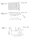
- FIG. 1(b) an energy band diagram of this structure is shown in FIG. 1(b). That is, a quantum well 48 which corresponds to the well layer 44 is sandwiched between barrier layers 46 of valence and conduction bands corresponding to the barrier layer 42, and well-type potential continues.
- the width L W of this well is as small as several 10 nm, the motion of the electrons and holes inside the well layer 44 in the z direction is limited, and respective energy levels are quantized.
- a well in such state is called a quantum well (QW), and a plurality of such wells when connected are called a multi-quantum well (MQW).
- QW quantum well
- MQW multi-quantum well
- a quantum well having such optical characteristics is utilized in optical devices such as optical modulators, optical bistable devices, and optical switches.
- a conventional optical modulator is a diode formed by an arrangement in which an active layer 50 formed from a MQW, in which the barrier layer 42 and the well layer 44 are laminated, is interposed between a p-type semiconductor 52 and an n-type semiconductor 54, as shown in FIG. 1(c).
- a p-type semiconductor 52 and the n-type semiconductor 54 InP, etc. is used.
- the energy band diagram of this diode is the same as that shown in FIG. 1(b). When a reverse bias is applied to this diode, the energy band diagram varies as shown in FIG. 1(d). That is, the energy level of the quantized electrons and holes in the quantum well 48 sandwiched by barrier walls 46 are decreased.
- the optical absorption spectrum is shown by the spectrum indicated by the broken line in FIG. 2.
- the absorption peak due to an exciton associated with an electron and a hole shifts several 10 meV toward the long wavelength side, i.e., a low energy side. This is called an electric-field on state.
- the light emission wavelength ⁇ L1 of a semiconductor laser has been set to a position indicated by an arrow in FIG. 2, i.e., to the optical absorption peak A′ of an exciton near the absorption edge in the electric-field on state.
- Optical modulation can be performed by causing this laser beam to enter the MQW active layer 50 of an optical modulator in which the electric field is turned on and off. That is, a laser beam is emitted from the MQW active layer 50 at a light intensity of I OFF , scarcely being absorbed in the off state. In the on state, however, the laser beam is absorbed in the quantum well 48 of the MQW active layer 50, and a light intensity I ON at which light is emitted on the outside is small.
- the strength of optical absorption due to an exciton should be as large as possible.
- a conventional optical bistable device is one called SEED (self electro-optic effect device) in which the diode shown in FIG. 1(c) is connected to a power supply via an external load resistance.
- SEED self electro-optic effect device
- an incident beam is made to enter from a p-type semiconductor layer and an emission beam is caused to be emitted from an n-type semiconductor layer.
- a reverse bias is applied to the SEED beforehand, and the wavelength ⁇ L2 of the incident beam is set to the wavelength of an exciton absorption A in the electric-field off state.
- This incident beam is absorbed in the quantum well 48 of the MQW active layer 50, and a photoelectric current flows in the SEED at almost 100% efficiency.
- the reverse bias voltage applied to the diode is decreased, and the optical absorption spectrum shown in FIG. 2 nears the solid line, i.e., the electric-field off state. Therefore, an optical absorption coefficient with respect to the incident beam is increased, thus causing a photoelectric current to increase and causing the reverse bias voltage to further decrease.
- optical bistable characteristics can be observed between the incident beam and the emission beam.
- the width of this bistable area depends on the ratio of the absorption coefficient of the exciton absorption A indicated by the solid line in FIG. 2 to the absorption coefficient of the spectra indicated by the broken line corresponding to the wavelength ⁇ L2 of the incident beam. The larger the ratio, the wider the bistable area.
- FIG. 3 explains an example of an optical switch using a diode having an MQW 60 as in FIG. 1(c).
- An n-type InP layer 63 and a p-type InP island 62 are formed on an n-type InP substrate 64 via the MQW 60.
- an X waveguide 61 of an n-type InP layer is disposed with the p-type InP island 62 in the middle.
- the black section of the upper section of the figure denotes an electrode.
- An incident beam I propagates along the waveguide and travels straight as a transmission beam T in a case where an electric field is not applied to the MQW.
- the optical absorption strength of an exciton should preferably be maximal in optical modulators, in optical bistable devices, and in optical switches.
- the optical absorption coefficient of an exciton is 1x104cm ⁇ 1 at most at room temperature, and in the case of InGaAs, it is 8x103cm ⁇ 1.
- the value of the exciton absorption coefficient must be further increased by 10% or more. A larger value of the absorption coefficient has also been desired to improve optical bistable device characteristics.
- An object of the present invention is to improve the characteristics of an optical semiconductor device.
- Another object of the present invention is to increase the optical absorption strength of an exciton in a III-V compound semiconductor.
- Compressive or tensile strain is introduced into a well layer by providing a difference between the lattice constants of a well layer and a barrier layer forming an MQW structure.
- the oscillator strength of an exciton is increased by causing the effective mass of a heavy hole inside a quantum well to be larger in order to increase the optical absorption coefficient.
- the band of a light hole is positioned above that of the heavy hole. This is made interchanging the position of the absorption peak due to an exciton associated with an electron and a heavy hole with the position of the absorption peak due to an exciton associated with an electron and a light hole.
- the ratio of the absorption coefficient due to an exciton near the absorption edge to the absorption coefficient of a low absorption region on the short wavelength side is thus increased.
- an MQW active layer is formed from an In 1-x Ga x As well layer and an InP barrier layer.
- the composition x of the In 1-x Ga x As well layer is made smaller than the composition whose lattices are matched with InP in order to increase its lattice constant, and a compressive strain is introduced into the In 1-x Ga x As well layer.
- an oscillator strength in a wavelength i.e., optical absorption strength, can be increased. Modulation efficiency is enhanced as the result of the production of a p-n diode light modulator in which such MQW active layer is disposed.
- the composition x of the In 1-x Ga x As well layer is made larger than the composition whose lattices are matched with InP in order to decrease its lattice constant, and a tensile strain is introduced into the In 1-x Ga x As well layer.
- the shift of the absorption peak due to an exciton associated with an electron and a light hole to the long wavelength side of the absorption peak wavelength due to an exciton associated with an electron and a heavy hole enables the ratio of the optical absorption coefficient in the optical absorption peak wavelength of an exciton associated with an electron and a heavy hole to the optical absorption coefficient in the low absorption region of the short wavelength side to be increased.
- an optical bistable characteristic which is more stable than was previously possible, can be obtained as the result of the production of an optical bistable device having an MQW active layer using such an In 1-x Ga x As well layer and an InP barrier layer.
- FIGS. 4(a) through 5(c) are views for explaining the principles of the present invention.
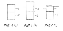
- FIGS. 4(a) to 4(c) are schematic views illustrating the crystal lattices of two types of laminated semiconductor layers (a barrier layer 2 and a well layer 4).
- FIGS. 4(a) to 4(c) are schematic views illustrating the band structure of the quantum wells which correspond to the crystal lattices of FIGS. 4(a) to 4(c).
- FIG. 4(a) the lattice constants of the barrier layer 2 and the well layer 4 are equal to each other, which indicates that their lattices are matched.
- FIG. 5(a) is an E-K curve in a direction of the in-plane of the quantum well of the well layer 4.
- the conduction band CB is almost parabolic.
- FIG. 4(b) shows a case where the lattice constant of the well layer 4 is greater than that of the barrier layer 2.
- FIG. 4(c) shows a case where the lattice constant of the well layer 4 is smaller than that of the barrier layer 2.
- a tensile strain occurs in the well layer 4 so as to cause the lattice constant of the in-plane in contact with the barrier layer 2 to be in agreement with that of the well layer 4.
- the band LH of the light hole is positioned above the band HH of the heavy hole, as in the E-K curve shown in FIG. 5(c).
- the position of the absorption peak due to an exciton associated with an electron and a heavy hole is interchanged with the position of the absorption peak due to an exciton associated with an electron and a light hole.
- the laminated structure of an InGaAs well layer and an InP barrier layer is produced. It is confirmed that the oscillator strength of an exciton is increased and the ratio of an absorption peak due to an exciton associated with an electron and a heavy hole to the absorption coefficient of a low absorption region on a shorter wavelength side than the peak,is increased with the lamination of the structure.
- FIG. 6 is a perspective view illustrating an optical modulator in the first embodiment.
- a laser beam of a wavelength ⁇ L is incident on an MQW active layer 6 interposed between a p-type InP 8 and an n-type InP 10 in the direction shown (in parallel to the MQW plane).
- a p-side electrode 12 and an n-side electrode 14 are disposed on the top surface of the p-type InP 8 and the bottom surface of the n-type InP 10, respectively.
- the MQW active layer 6 is formed from a lamination structure in which the In 1-x Ga x As well layer and an InP barrier layer are laminated.
- the thickness of the In 1-x Ga x As well layer is about 10nm.
- the value x representing the composition of the In 1-x Ga x As well layer is set at 0.44, which is chosen to be smaller than the x value 0.47 of a composition at which the lattice of the In 1-x Ga x As well layer is matched with that of the InP barrier layer, so that the lattice constant of the In 1-x Ga x As well layer is greater than that of the InP barrier layer.
- a compressive strain is introduced into the In 0.56 Ga 0.44 As well layer.
- the value x can range from 0.35 to 0.60
- FIG. 7(a) shows the optical absorption spectrum of an MQW active layer 6 consisting of a lamination structure of an In 0.56 Ga 0.44 As well layer and an InP barrier layer at room temperature.
- FIG. 7(b) shows, for comparison, the optical absorption spectrum of an MQW active layer 6 consisting of a lamination structure of an In 0.53 Ga 0.47 well layer and an InP barrier layer at room temperature, in which the lattice of the In 1-x Ga x As well layer is matched with that of the InP barrier layer.
- FIG. 8 is a graph in which is plotted the relation between an exciton optical absorption intensity and the absorption peak wavelength ⁇ P of an exciton at 77K temperature with respect to several In 1-x Ga x As well layers having different composition x.
- FIG. 9 is a graph in which is plotted the relation between ⁇ E and the absorption peak wavelength ⁇ P of an exciton at 77K temperature with respect to an In 1-x Ga x As well layers having a composition value x of 0.42 to 0.52.
- the solid line denotes the calculated value of ⁇ E of the In 1-x Ga x As well layer with respect to the composition x, the band gap variation and the amount of strain being taken into consideration.
- the measurement value of ⁇ E is quite in agreement with the calculation value. This fact indicates that a strain in accordance with a theory is introduced to the In 1-x Ga x As well layer in correspondence with the value of the composition x.
- the composition x of the In 1-x Ga x As well layer is made smaller than the composition value at which lattices are matched, and a compressive strain is introduced into the In 1-x Ga x As well layer.
- the amount of strain required to increase the effective mass of the band of an electron and a heavy hole to increase the exciton strength and its sense depends on the kind of a material used in the MQW. Consequently, if an amount and sense of strain is controlled in an arbitrary MQW, it is possible to increase the exciton strength.
- FIG. 10 is a schematic view of the SEED in the second embodiment.
- An MQW active layer 20 in which an In 1-x Ga x As well layer 16 and an InP barrier layer 18 are alternately laminated is interposed between a p-type InP layer 22 and an n-type InP layer 24, thus a diode is formed.
- a power supply V for applying a reverse bias is connected to this diode via an external load resistance R.
- the thickness of the In 1-x Ga x As well layer 16 is about 10 nm.
- the composition x is set at 0.55 so that the lattice constant of the In 1-x Ga x As well layer 16 is smaller than the lattice constant of the InP barrier layer 18. As a result, a tensile strain is introduced to the In 1-x Ga x As well layer 16.
- the well layer thickness can be from about 5 nm to 15 nm.
- An incident beam of a power of P IN is entered from above the p-type InP layer 22, and an emission beam of power P OUT is emitted beneath the n-type InP layer 24.
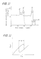
- FIG. 11 shows the optical absorption spectrum of an MQW constituting a SEED of FIG. 10.
- shown by the solid line is an optical absorption spectrum in a case where a tensile strain of an In 0.45 Ga 0.55 As well layer whose introduced.
- Shown by the broken line is the optical absorption spectrum of an In 0.56 Ga 0.44 As well layer whose lattice is matched with that of the InP barrier layer, which is shown for comparison.
- the optical absorption peak (the A region) due to an exciton associated with an electron and a heavy hole is present in the short wavelength side of the optical absorption peak (the B region) due to an exciton associated with an electron and a light hole.
- the optical absorption peak (the A′ region) due to an exciton associated with an electron and a heavy hole is present in the long wavelength side of the optical absorption peak (the B′ region) due to an exciton associated with an electron and a light hole.
- the position of the absorption peak A due to an exciton associated with an electron and a heavy hole is interchanged with the position of the absorption peak B due to an exciton associated with an electron and a light hole.
- an absorption coefficient in a low-absorption region in the wavelength shorter than the optical absorption peak wavelength ⁇ P of an exciton associated with an electron and a heavy hole in the A section is smaller than an optical absorption coefficient in a corresponding low-absorption region of the In 0.53 Ga 0.47 As well layer. Therefore, in the case of the In 0.45 Ga 0.55 As well layer, the ratio of an optical absorption coefficient in the peak wavelength ⁇ P to that in the low-absorption region of the short wavelength side is greater than in the case of the In 0.53 Ga 0.47 As well layer.
- FIG. 12 is a graph for explaining the bistable characteristics of the above-mentioned SEED, in which the optical bistable characteristics between an incident beam power (P IN ) and an emission beam power (P OUT ) are shown.
- the width (W) of this bistable area is larger than in the first embodiment, since the ratio of the optical absorption coefficient at the peak wavelength ⁇ P to the optical absorption coefficient in the low-absorption region of the short wavelength side is greater than in the case of the In 0.53 Ga 0.47 As well layer. Consequently, an optical bistable operation can be performed stably.
- the present invention is not limited to an optical modulator and an optical bistable device.
- the present invention can also be applied to the other optical semiconductor devices such as optical switches.
Abstract
Description
- The present invention relates to an optical semiconductor device and, in particular, to an optical semiconductor device having a quantum well structure.
- The technology of so-called band engineering regarding a quantum well structure made up of III-V compound semiconductor thin layers, super lattices, strained lattices or the like have been developed considerably. Optical devices such as lasers, optical sensing devices, optical modulating devices, and the like, in which band engineering is applied, have recently come into practical use.
- Regarding a structure in which there are two types of semiconductor layer, i.e., a
barrier layer 42 and awell layer 44 shown in FIG. 1(a), an energy band diagram of this structure is shown in FIG. 1(b). That is, aquantum well 48 which corresponds to thewell layer 44 is sandwiched betweenbarrier layers 46 of valence and conduction bands corresponding to thebarrier layer 42, and well-type potential continues. When the width LW of this well is as small as several 10 nm, the motion of the electrons and holes inside thewell layer 44 in the z direction is limited, and respective energy levels are quantized. A well in such state is called a quantum well (QW), and a plurality of such wells when connected are called a multi-quantum well (MQW). - In the optical absorption spectrum of a bulk semiconductor material, generally, a sharp absorption peak is observed in the vicinity of the absorption edge at low temperatures. This absorption peak is due to an absorption caused by an exciton in which an electron and a hole are combined with each other by the Coulomb force. In a model of an exciton in which an electron is distributed spherically around a hole, its diameter is determined by the reduced effective mass of the exciton and the static dielectric constant of a semiconductor material, and is usually 20 to 40 nm.
- When an exciton is produced in the
quantum well 48, the bonding energy increases since the exciton is compressed in a direction perpendicular to thewell layer 44, thus causing an increase in the oscillator strength of the exciton, i.e., the strength of optical absorption. A clear optical absorption peak is observed even at room temperature. An actually observed optical absorption spectrum is schematically shown in FIG. 2. - In FIG. 2, an absorption peak due to an exciton associated with an electron and a heavy hole is observed in the portion indicated by the letter A, and an absorption peak due to an exciton associated with an electron and a light hole is observed in the portion indicated by the letter B.
- A quantum well having such optical characteristics is utilized in optical devices such as optical modulators, optical bistable devices, and optical switches.
- A conventional optical modulator is a diode formed by an arrangement in which an
active layer 50 formed from a MQW, in which thebarrier layer 42 and thewell layer 44 are laminated, is interposed between a p-type semiconductor 52 and an n-type semiconductor 54, as shown in FIG. 1(c). For the p-type semiconductor 52 and the n-type semiconductor 54, InP, etc. is used. The energy band diagram of this diode is the same as that shown in FIG. 1(b). When a reverse bias is applied to this diode, the energy band diagram varies as shown in FIG. 1(d). That is, the energy level of the quantized electrons and holes in thequantum well 48 sandwiched bybarrier walls 46 are decreased. For this reason, the optical absorption spectrum is shown by the spectrum indicated by the broken line in FIG. 2. The absorption peak due to an exciton associated with an electron and a hole shifts several 10 meV toward the long wavelength side, i.e., a low energy side. This is called an electric-field on state. - Suppose that the light emission wavelength λL1 of a semiconductor laser has been set to a position indicated by an arrow in FIG. 2, i.e., to the optical absorption peak A′ of an exciton near the absorption edge in the electric-field on state. Optical modulation can be performed by causing this laser beam to enter the MQW
active layer 50 of an optical modulator in which the electric field is turned on and off. That is, a laser beam is emitted from the MQWactive layer 50 at a light intensity of IOFF, scarcely being absorbed in the off state. In the on state, however, the laser beam is absorbed in thequantum well 48 of the MQWactive layer 50, and a light intensity ION at which light is emitted on the outside is small. The intensity ratio η (=ION/IOFF) of an emission laser beam which is emitted in correspondence to the on or off state of an electric field should preferably be minimal from the viewpoint of modulation characteristics. For that purpose, the strength of optical absorption due to an exciton should be as large as possible. - A conventional optical bistable device is one called SEED (self electro-optic effect device) in which the diode shown in FIG. 1(c) is connected to a power supply via an external load resistance. In the SEED, an incident beam is made to enter from a p-type semiconductor layer and an emission beam is caused to be emitted from an n-type semiconductor layer. Now, a reverse bias is applied to the SEED beforehand, and the wavelength λL2 of the incident beam is set to the wavelength of an exciton absorption A in the electric-field off state. This incident beam is absorbed in the
quantum well 48 of the MQWactive layer 50, and a photoelectric current flows in the SEED at almost 100% efficiency. As a result, the reverse bias voltage applied to the diode is decreased, and the optical absorption spectrum shown in FIG. 2 nears the solid line, i.e., the electric-field off state. Therefore, an optical absorption coefficient with respect to the incident beam is increased, thus causing a photoelectric current to increase and causing the reverse bias voltage to further decrease. As the result of the occurrence of such a positive feedback, optical bistable characteristics can be observed between the incident beam and the emission beam. The width of this bistable area depends on the ratio of the absorption coefficient of the exciton absorption A indicated by the solid line in FIG. 2 to the absorption coefficient of the spectra indicated by the broken line corresponding to the wavelength λL2 of the incident beam. The larger the ratio, the wider the bistable area. - FIG. 3 explains an example of an optical switch using a diode having an
MQW 60 as in FIG. 1(c). An n-type InP layer 63 and a p-type InP island 62 are formed on an n-type InP substrate 64 via theMQW 60. Further, anX waveguide 61 of an n-type InP layer is disposed with the p-type InP island 62 in the middle. The black section of the upper section of the figure denotes an electrode. An incident beam I propagates along the waveguide and travels straight as a transmission beam T in a case where an electric field is not applied to the MQW. Conversely, when an electric field is applied to the MQW, since the exciton absorption peak shifts toward the long wavelength side, the index of refraction varies. As a result, the incident beam travels along another waveguide as a refraction beam R. The stronger absorption intensity by the exciton, the larger the variation in the index of refraction, and therefore switching characteristics are better. - As described above, the optical absorption strength of an exciton should preferably be maximal in optical modulators, in optical bistable devices, and in optical switches. In the case of a III-V compound semiconductor, the optical absorption coefficient of an exciton is 1x10⁴cm⁻¹ at most at room temperature, and in the case of InGaAs, it is 8x10³cm⁻¹. To obtain excellent characteristics of an optical modulator, the value of the exciton absorption coefficient must be further increased by 10% or more. A larger value of the absorption coefficient has also been desired to improve optical bistable device characteristics.
- An object of the present invention is to improve the characteristics of an optical semiconductor device.
- Another object of the present invention is to increase the optical absorption strength of an exciton in a III-V compound semiconductor.
- The above-mentioned objects can be achieved by using the optical semiconductor device defined in
claim 1. - Compressive or tensile strain is introduced into a well layer by providing a difference between the lattice constants of a well layer and a barrier layer forming an MQW structure. The oscillator strength of an exciton is increased by causing the effective mass of a heavy hole inside a quantum well to be larger in order to increase the optical absorption coefficient. Then the band of a light hole is positioned above that of the heavy hole. This is made interchanging the position of the absorption peak due to an exciton associated with an electron and a heavy hole with the position of the absorption peak due to an exciton associated with an electron and a light hole. The ratio of the absorption coefficient due to an exciton near the absorption edge to the absorption coefficient of a low absorption region on the short wavelength side is thus increased.
- The above is realized as follows: an MQW active layer is formed from an In1-xGaxAs well layer and an InP barrier layer. The composition x of the In1-xGaxAs well layer is made smaller than the composition whose lattices are matched with InP in order to increase its lattice constant, and a compressive strain is introduced into the In1-xGaxAs well layer. Thus, regarding the absorption peak due to an exciton associated with an electron and a heavy hole, an oscillator strength in a wavelength, i.e., optical absorption strength, can be increased. Modulation efficiency is enhanced as the result of the production of a p-n diode light modulator in which such MQW active layer is disposed.
- Conversely, the composition x of the In1-xGaxAs well layer is made larger than the composition whose lattices are matched with InP in order to decrease its lattice constant, and a tensile strain is introduced into the In1-xGaxAs well layer. Thus, the shift of the absorption peak due to an exciton associated with an electron and a light hole to the long wavelength side of the absorption peak wavelength due to an exciton associated with an electron and a heavy hole enables the ratio of the optical absorption coefficient in the optical absorption peak wavelength of an exciton associated with an electron and a heavy hole to the optical absorption coefficient in the low absorption region of the short wavelength side to be increased. Consequently, a wider bistable area, i.e., an optical bistable characteristic which is more stable than was previously possible, can be obtained as the result of the production of an optical bistable device having an MQW active layer using such an In1-xGaxAs well layer and an InP barrier layer.
- These and other objects, features and advantages of the present invention will become clear when reference is made to the following description of the preferred embodiments of the present invention, together with reference to the accompanying drawings.
-
- FIG. 1(a) is a cross-sectional schematic view illustrating a structure in which a barrier layer and a well layer are laminated;
- FIG. 1(b) is an energy band which corresponds to the structure in FIG. 1(a);
- FIG. 2 is a view schematically illustrating an optical absorption spectrum for explaining a conventional optical modulator;
- FIG. 1(c) is a cross-sectional schematic view for explaining the conventional optical modulator;
- FIG. 1(d) is an energy band diagram in a case where a reverse bias is applied to the diode of FIG. 1(c);
- FIG. 3 is a view for explaining a conventional optical switching device;
- FIG. 4(a) is a schematic view illustrating the crystal lattices of a barrier layer and a well layer in a case where the lattice constant of the barrier layer is equal to that of the well layer;
- FIG. 4(b) is a schematic view illustrating the crystal lattices of a barrier layer and a well layer in a case where the lattice constant of the well layer is greater than that of the barrier layer;
- FIG. 4(c) is a schematic view illustrating the crystal lattices of a barrier layer and a well layer in a case where the lattice constant of the well layer is smaller than that of the barrier layer;
- FIG. 5 (a) is an energy wave number (E-K) curve in the direction of the in-plane of the quantum well of the well layer;
- FIG. 5(b) is an E-K curve of an well layer having compressive strain;
- FIG. 5(c) is an E-K curve of an well layer having tensile strain;
- FIG. 6 is a perspective view illustrating an optical modulator in a first embodiment;
- FIG. 7(a) is a view showing an optical absorption spectrum of an MQW active layer consisting of a lamination structure of an In0.56Ga0.44As well layer and an InP barrier layer at room temperature;
- FIG. 7(b) is a view showing an optical absorption spectrum of an MQW
active layer 6 consisting of a lamination structure of an In0.53Ga0.47As well layer and an InP barrier layer at room temperature; - FIG. 8 is a graph in which is plotted the relation between an exciton optical absorption intensity and an absorption peak wavelength λPat 77K temperature with respect to several In1-xGaxAs well layers having different composition
- FIG. 9 is a graph in which is plotted the relation between ΔE and the absorption peak wavelength λP of an exciton at 77K temperature with respect to several In1-xGaxAs well layers having different composition x;
- FIG. 10 is a schematic view of a SEED in a second embodiment;
- FIG. 11 is a view illustrating the optical absorption spectrum of an MQW constituting the SEED for explaining the characteristics of the SEED of FIG. 10; and
- FIG. 12 is a graph for explaining the bistable characteristics of the SEED of FIG. 10.
- Two embodiments of the present invention will be explained hereunder with reference to FIGS. 4 through 12.
- In all the views, like numerals and characters designate like or corresponding parts.
- This is an embodiment in which the present invention is applied to an optical modulator.
- FIGS. 4(a) through 5(c) are views for explaining the principles of the present invention.
- FIGS. 4(a) to 4(c) are schematic views illustrating the crystal lattices of two types of laminated semiconductor layers (a
barrier layer 2 and a well layer 4). FIGS. 4(a) to 4(c) are schematic views illustrating the band structure of the quantum wells which correspond to the crystal lattices of FIGS. 4(a) to 4(c). - In FIG. 4(a), the lattice constants of the
barrier layer 2 and thewell layer 4 are equal to each other, which indicates that their lattices are matched. FIG. 5(a) is an E-K curve in a direction of the in-plane of the quantum well of thewell layer 4. In FIG. 5, the conduction band CB is almost parabolic. In the valence band, the band HH of a heavy hole and the band LH of a light hole are split at K = 0; at K > 0, the band HH of the heavy hole is positioned above the band LH of the light hole. FIG. 4(b) shows a case where the lattice constant of thewell layer 4 is greater than that of thebarrier layer 2. In this case, as shown by the broken line, a compressive strain occurs in thewell layer 4 so as to cause the lattice constant of the in-plane in contact with thebarrier layer 2 to be in agreement with that of thewell layer 4. In the E-K curve of thewell layer 4 having such a strain, as shown in FIG. 5(b), the position of the band of a hole moves at the point K = 0, and an energy difference (ΔE) between the band HH of the heavy hole and the band LH of the light hole becomes greater. - FIG. 4(c) shows a case where the lattice constant of the
well layer 4 is smaller than that of thebarrier layer 2. In this case, as shown by the broken line, a tensile strain occurs in thewell layer 4 so as to cause the lattice constant of the in-plane in contact with thebarrier layer 2 to be in agreement with that of thewell layer 4. In the E-K curve of thewell layer 4 having such a strain, the position of the band of a hole moves at the point K = 0, and the ΔE becomes smaller. Depending upon the magnitude of a tensile strain which occurs in thewell layer 4, the band LH of the light hole is positioned above the band HH of the heavy hole, as in the E-K curve shown in FIG. 5(c). As a result, in the optical absorption spectrum, the position of the absorption peak due to an exciton associated with an electron and a heavy hole is interchanged with the position of the absorption peak due to an exciton associated with an electron and a light hole. - Since the effect of these two types of strains causes the magnitude of the interaction between the band HH of the heavy hole and the band LH of the light hole to vary, the shapes of the bands themselves vary, as shown in FIG. 5(b). How the shape of a band varies depending on the sense and magnitude of a strain is determined by the properties of the material from which a quantum well is formed.
- Meanwhile, the fact that the oscillator strength of an exciton depends on the shape of a band in the vicinity of K = 0 is known from quantum mechanics. That is, in the case of an upward convex as the band HH of the heavy hole, the smaller (i.e., the greater the effective mass) the absolute value of a rate of change with respect to the wave number K of an energy E, the greater the oscillator strength. Conversely, in the case of a downward convex as the band LH of the light hole, the greater (i.e., the smaller the effective mass) the absolute value of a rate of change with respect to the wave number K of an energy E, the greater the oscillator strength. Therefore, the oscillator strength of an exciton can be increased with a method wherein a strain is intentionally introduced to the
well layer 4, and the shape of the band of a hole can thus be optimized. - As shown in FIG. 5(c), where a tensile strain is applied and thus the band LH of the light hole is positioned above the band HH of the heavy hole, the position of the absorption peak due to an exciton associated with an electron and a heavy hole moves to the short wavelength side of the absorption peak due to an exciton associated with an electron and a light hole. As a result, the ratio of the absorption peak due to an exciton associated with an electron and the heavy hole to the absorption coefficient of a low absorption region on a shorter wavelength side than the peak is greater than in a case where no tensile strain is applied.
- To utilize the principles described above, the laminated structure of an InGaAs well layer and an InP barrier layer is produced. It is confirmed that the oscillator strength of an exciton is increased and the ratio of an absorption peak due to an exciton associated with an electron and a heavy hole to the absorption coefficient of a low absorption region on a shorter wavelength side than the peak,is increased with the lamination of the structure.
- FIG. 6 is a perspective view illustrating an optical modulator in the first embodiment. In the optical modulator shown in FIG. 6, a laser beam of a wavelength λL is incident on an MQW
active layer 6 interposed between a p-type InP 8 and an n-type InP 10 in the direction shown (in parallel to the MQW plane). A p-side electrode 12 and an n-side electrode 14 are disposed on the top surface of the p-type InP 8 and the bottom surface of the n-type InP 10, respectively. The MQWactive layer 6 is formed from a lamination structure in which the In1-xGaxAs well layer and an InP barrier layer are laminated. The thickness of the In1-xGaxAs well layer is about 10nm. The value x representing the composition of the In1-xGaxAs well layer is set at 0.44, which is chosen to be smaller than the x value 0.47 of a composition at which the lattice of the In1-xGaxAs well layer is matched with that of the InP barrier layer, so that the lattice constant of the In1-xGaxAs well layer is greater than that of the InP barrier layer. As a result, a compressive strain is introduced into the In0.56Ga0.44As well layer. Generally, the value x can range from 0.35 to 0.60 - FIG. 7(a) shows the optical absorption spectrum of an MQW
active layer 6 consisting of a lamination structure of an In0.56Ga0.44As well layer and an InP barrier layer at room temperature. FIG. 7(b) shows, for comparison, the optical absorption spectrum of an MQWactive layer 6 consisting of a lamination structure of an In0.53Ga0.47 well layer and an InP barrier layer at room temperature, in which the lattice of the In1-xGaxAs well layer is matched with that of the InP barrier layer. - As is apparent from a comparison of FIG. 7(a) with FIG. 7(b), the optical absorption peak wavelength λP due to an exciton associated with an electron and a heavy hole in In0.56Ga0.44As well shifts toward the long wavelength side, and the peak value at the wavelength λP is greater. For this reason, an exciton peak region representing the oscillator strength of an exciton is greater. In addition, it is confirmed that the ΔE corresponding to a difference between an optical absorption peak due to an exciton associated with an electron and a heavy hole and an optical absorption peak due to an exciton associated with an electron and a light hole is greater.
- Next, to make clear how the optical absorption strength of an exciton associated with an electron and a heavy hole varies with the variation in the composition x of the In1-xGaxAs well layer, the results of the measurement of the variation in the exciton optical absorption strength when the value of the composition x varies in a direction in which it becomes smaller are shown in FIG. 8. FIG. 8 is a graph in which is plotted the relation between an exciton optical absorption intensity and the absorption peak wavelength λP of an exciton at 77K temperature with respect to several In1-xGaxAs well layers having different composition x. In FIG. 8, it can be seen that the exciton optical absorption strength ,when the composition x is 0.47, is 100 to 110 ev/cm; when the composition x is between 0.43 and 0.46, the exciton optical absorption strength is between 120 and 130 eV/cm, which is an increase of 20 to 30% in comparison with the case of x = 0.47.
- Therefore, when the wavelength λL of a laser beam incident on the MQW
active layer 6 of an optical modulator shown in FIG. 6 is set to the optical absorption peak wavelength λP of an optical absorption peak due to an exciton associated with an electron and a heavy hole in FIG. 7 (a), the laser beam intensity ratio η (=ION/IOFF) in correspondence to the on or off state of an electric field can be made smaller than in a case where the wavelength λL is set to λP in FIG. 7(b). - Next, to make clear how the energy difference ΔE between an energy corresponding to an optical absorption peak due to an exciton associated with an electron and a heavy hole and an absorption peak due to an exciton associated with an electron and a light hole varies with the variation in the composition x of the In1-xGaxAs well layer, ΔE is measured with respect to an In1-xGaxAs well layer of various compositions, the results of which are shown in FIG. 9. FIG. 9 is a graph in which is plotted the relation between ΔE and the absorption peak wavelength λP of an exciton at 77K temperature with respect to an In1-xGaxAs well layers having a composition value x of 0.42 to 0.52. In this graph, the solid line denotes the calculated value of ΔE of the In1-xGaxAs well layer with respect to the composition x, the band gap variation and the amount of strain being taken into consideration. As apparent from this figure, the measurement value of ΔE is quite in agreement with the calculation value. This fact indicates that a strain in accordance with a theory is introduced to the In1-xGaxAs well layer in correspondence with the value of the composition x.
- In this embodiment, a case is described where the composition x of the In1-xGaxAs well layer is made smaller than the composition value at which lattices are matched, and a compressive strain is introduced into the In1-xGaxAs well layer. The amount of strain required to increase the effective mass of the band of an electron and a heavy hole to increase the exciton strength and its sense (compressive or tensile) depends on the kind of a material used in the MQW. Consequently, if an amount and sense of strain is controlled in an arbitrary MQW, it is possible to increase the exciton strength.
- An example in which the present invention is applied to a SEED will be explained. FIG. 10 is a schematic view of the SEED in the second embodiment. An MQW active layer 20 in which an In1-xGaxAs well
layer 16 and an InP barrier layer 18 are alternately laminated is interposed between a p-type InP layer 22 and an n-type InP layer 24, thus a diode is formed. A power supply V for applying a reverse bias is connected to this diode via an external load resistance R. - The thickness of the In1-xGaxAs well
layer 16 is about 10 nm. The composition x is set at 0.55 so that the lattice constant of the In1-xGaxAs welllayer 16 is smaller than the lattice constant of the InP barrier layer 18. As a result, a tensile strain is introduced to the In1-xGaxAs welllayer 16. Generally, the well layer thickness can be from about 5 nm to 15 nm. - An incident beam of a power of PIN is entered from above the p-
type InP layer 22, and an emission beam of power POUT is emitted beneath the n-type InP layer 24. - FIG. 11 shows the optical absorption spectrum of an MQW constituting a SEED of FIG. 10. In FIG. 11, shown by the solid line is an optical absorption spectrum in a case where a tensile strain of an In0.45Ga0.55As well layer whose introduced. Shown by the broken line is the optical absorption spectrum of an In0.56Ga0.44As well layer whose lattice is matched with that of the InP barrier layer, which is shown for comparison. As can be seen from this figure, in the case of the In0.45Ga0.55As well layer of the optical absorption peak wavelength λP ,due to an exciton associated with an electron and a heavy hole in the A region, has been shifted to the longer wavelength side in comparison with the A′ region of the In0.53Ga0.47As well layer. There is also a sharp peak, though small, present in the B region in the vicinity of the absorption edge on the longer wavelength side of the peak wavelength λP. This peak is the optical absorption peak due to an exciton associated with an electron and a light hole. In the case of the In0.45Ga0.55As well layer, the optical absorption peak (the A region) due to an exciton associated with an electron and a heavy hole is present in the short wavelength side of the optical absorption peak (the B region) due to an exciton associated with an electron and a light hole. On the other hand, in the case of the In0.53Ga0.47As well layer, the optical absorption peak (the A′ region) due to an exciton associated with an electron and a heavy hole is present in the long wavelength side of the optical absorption peak (the B′ region) due to an exciton associated with an electron and a light hole. Thus , as the result of the introduction of tensile strain to the In1-xGaxAs well layer, the position of the absorption peak A due to an exciton associated with an electron and a heavy hole is interchanged with the position of the absorption peak B due to an exciton associated with an electron and a light hole.
- As a result, in the case of the In0.45Ga0.55As well layer, an absorption coefficient in a low-absorption region in the wavelength shorter than the optical absorption peak wavelength λP of an exciton associated with an electron and a heavy hole in the A section is smaller than an optical absorption coefficient in a corresponding low-absorption region of the In0.53Ga0.47As well layer. Therefore, in the case of the In0.45Ga0.55As well layer, the ratio of an optical absorption coefficient in the peak wavelength λP to that in the low-absorption region of the short wavelength side is greater than in the case of the In0.53Ga0.47As well layer.
- FIG. 12 is a graph for explaining the bistable characteristics of the above-mentioned SEED, in which the optical bistable characteristics between an incident beam power (PIN) and an emission beam power (POUT) are shown. In the case of the In0.45Ga0.55As well layer, the width (W) of this bistable area is larger than in the first embodiment, since the ratio of the optical absorption coefficient at the peak wavelength λP to the optical absorption coefficient in the low-absorption region of the short wavelength side is greater than in the case of the In0.53Ga0.47As well layer. Consequently, an optical bistable operation can be performed stably.
- In the first and second embodiments, a case where an MQW active layer in which an In1-xGaxAs well layer and an InP barrier layer are alternately laminated is described. The same advantage as above can be obtained by the use of an MQW active layer in which an In1-xGaxAs1-yPy well layer and an InP barrier layer are alternately laminated.
- The present invention is not limited to an optical modulator and an optical bistable device. The present invention can also be applied to the other optical semiconductor devices such as optical switches.
Claims (10)
a barrier layer having a definite lattice constant; and
a well layer having a lattice constant different from the lattice constant of said barrier layer, wherein an optical absorption intensity, is increased, due to at least one exciton produced in said well layer because of lattice strain caused in said well layer.
a barrier layer having a definite lattice constant; and
a well layer having a lattice constant smaller than the lattice constant of said barrier layer, wherein the position of the optical absorption peak due to an exciton associated with an electron and a heavy hole produced in said well layer is caused to occur on the shorter wavelength side than the position of the optical absorption peak due to an exciton associated with an electron and a light hole because of tensile strain which occurs in said well layer.
Applications Claiming Priority (4)
| Application Number | Priority Date | Filing Date | Title |
|---|---|---|---|
| JP24981489 | 1989-09-26 | ||
| JP249814/89 | 1989-09-26 | ||
| JP2070009A JPH03174790A (en) | 1989-09-26 | 1990-03-20 | Optical semiconductor element |
| JP70009/90 | 1990-03-20 |
Publications (3)
| Publication Number | Publication Date |
|---|---|
| EP0420749A2 true EP0420749A2 (en) | 1991-04-03 |
| EP0420749A3 EP0420749A3 (en) | 1991-12-18 |
| EP0420749B1 EP0420749B1 (en) | 1997-03-12 |
Family
ID=26411184
Family Applications (1)
| Application Number | Title | Priority Date | Filing Date |
|---|---|---|---|
| EP90402653A Expired - Lifetime EP0420749B1 (en) | 1989-09-26 | 1990-09-26 | Optical semiconductor device |
Country Status (4)
| Country | Link |
|---|---|
| US (1) | US5136602A (en) |
| EP (1) | EP0420749B1 (en) |
| JP (1) | JPH03174790A (en) |
| DE (1) | DE69030148T2 (en) |
Cited By (7)
| Publication number | Priority date | Publication date | Assignee | Title |
|---|---|---|---|---|
| GB2281785A (en) * | 1993-09-09 | 1995-03-15 | Northern Telecom Ltd | Electro absorption optical modulators |
| GB2282670A (en) * | 1993-10-05 | 1995-04-12 | Mitsubishi Electric Corp | Semiconductor optical modulator |
| EP0689230A3 (en) * | 1994-06-21 | 1996-07-03 | At & T Corp | Method for lattice matched growth of semiconductor layers |
| EP0721241A2 (en) * | 1995-01-04 | 1996-07-10 | Canon Kabushiki Kaisha | Semiconductor quantum well structure and semiconductor device using the same |
| WO1996027146A1 (en) * | 1995-02-28 | 1996-09-06 | Siemens Aktiengesellschaft | Integrated optical fibre with an optical layer having a controllable complex refraction index |
| GB2307784A (en) * | 1995-11-28 | 1997-06-04 | Toshiba Cambridge Res Center | Bistable optical semiconductor device |
| US5963358A (en) * | 1995-04-26 | 1999-10-05 | Kabushiki Kaisha Toshiba | Semiconductor device and method for its operation |
Families Citing this family (13)
| Publication number | Priority date | Publication date | Assignee | Title |
|---|---|---|---|---|
| JPH05145178A (en) * | 1991-11-18 | 1993-06-11 | Furukawa Electric Co Ltd:The | Strained quantum well semiconductor laser element |
| JP2953177B2 (en) * | 1992-03-11 | 1999-09-27 | 住友電気工業株式会社 | Multi-beam semiconductor laser and method of manufacturing the same |
| JP3306892B2 (en) * | 1992-02-28 | 2002-07-24 | 株式会社日立製作所 | Semiconductor optical integrated device and method of manufacturing the same |
| US5257276A (en) * | 1992-04-03 | 1993-10-26 | California Institute Of Technology | Strained layer InP/InGaAs quantum well laser |
| JPH07261220A (en) * | 1994-03-25 | 1995-10-13 | Atr Koudenpa Tsushin Kenkyusho:Kk | Semiconductor optical element |
| KR100363241B1 (en) * | 1995-05-25 | 2003-02-05 | 삼성전자 주식회사 | Multi-quantum well type laser diode and its manufacturing method |
| JP2002374042A (en) * | 2000-12-12 | 2002-12-26 | Fuji Photo Film Co Ltd | Semiconductor laser device |
| US7308202B2 (en) * | 2002-02-01 | 2007-12-11 | Cubic Corporation | Secure covert combat identification friend-or-foe (IFF) system for the dismounted soldier |
| WO2009009774A1 (en) * | 2007-07-11 | 2009-01-15 | Cubic Corporation | Integrated modulating retro-reflector |
| WO2009058890A2 (en) * | 2007-10-29 | 2009-05-07 | Cubic Corporation | Resonant quantum well modulator driver |
| US7859675B2 (en) * | 2007-11-06 | 2010-12-28 | Cubic Corporation | Field test of a retro-reflector and detector assembly |
| US20210036249A1 (en) * | 2019-08-02 | 2021-02-04 | The Florida State University Research Foundation, Incorporated | Systems and methods for bulk semiconductor sensitized solid state upconversion |
| FR3119710B1 (en) * | 2021-02-05 | 2023-04-28 | Lynred | Improved infrared detector via effective mass carrier engineering. |
Family Cites Families (7)
| Publication number | Priority date | Publication date | Assignee | Title |
|---|---|---|---|---|
| USRE22893E (en) * | 1947-06-24 | Manufacture of an improved | ||
| FR2620863B1 (en) * | 1987-09-22 | 1989-12-01 | Thomson Csf | OPTOELECTRONIC DEVICE BASED ON III-V COMPOUNDS ON SILICON SUBSTRATE |
| JPH0770743B2 (en) * | 1987-11-10 | 1995-07-31 | 富士通株式会社 | Resonant tunneling barrier structure device |
| US4941025A (en) * | 1987-12-30 | 1990-07-10 | Bell Communications Research, Inc. | Quantum well semiconductor structures for infrared and submillimeter light sources |
| JP2649936B2 (en) * | 1988-03-01 | 1997-09-03 | 富士通株式会社 | Strained superlattice buffer |
| US4984242A (en) * | 1989-09-18 | 1991-01-08 | Spectra Diode Laboratories, Inc. | GaAs/AlGaAs heterostructure laser containing indium |
| US4952792A (en) * | 1989-10-13 | 1990-08-28 | At&T Bell Laboratories | Devices employing internally strained asymmetric quantum wells |
-
1990
- 1990-03-20 JP JP2070009A patent/JPH03174790A/en active Pending
- 1990-09-25 US US07/587,686 patent/US5136602A/en not_active Expired - Lifetime
- 1990-09-26 EP EP90402653A patent/EP0420749B1/en not_active Expired - Lifetime
- 1990-09-26 DE DE69030148T patent/DE69030148T2/en not_active Expired - Fee Related
Non-Patent Citations (6)
| Title |
|---|
| APPLIED PHYSICS LETTERS. vol. 50, no. 7, 16 February 1987, NEW YORK US pages 368 - 370; U.KOREN ET AL.: 'InGaAs/InP MULTIPLE QUANTUM WELL WAVEGUIDE PHASE MODULATOR' * |
| APPLIED PHYSICS LETTERS. vol. 53, no. 9, 29 August 1988, NEW YORK US pages 731 - 733; SONGCHEOL HONG ET AL.: 'EFFECT OF THE LIFTING OF KRAMER'S DEGENERACY ON EXCITONIC LINEWIDTHS IN QUANTUM WELL OPTICAL MODULATORS' * |
| IEE PROCEEDINGS J. OPTOELECTRONICS vol. 136, no. 1, February 1989, STEVENAGE GB pages 46 - 51; D.R.P. GUY ET AL.: 'EXPERIMENTAL STUDY OF InGaAs-InP MQW ELECTRO-ABSORPTION MODULATORS' * |
| IEEE PHOTONICS TECHNOLOGY LETTERS vol. 1, no. 1, January 1989, NEW-YORK, US pages 19 - 20; K.WAKITA ET AL.: 'DYNAMIC FREQUENCY RESPONSE FOR InGaAs/InAlAs MULTIPLE QUANTUM WELL OPTICAL MODULATORS' * |
| OPTICAL ENGINEERING. vol. 26, no. 5, May 1987, BELLINGHAM US pages 368 - 372; D.A.B.MILLER: 'QUANTUM WELLS FOR OPTICAL INFORMATION PROCESSING' * |
| PROCEEDINGS OF THE 15TH SYMPOSIUM ON GALLIUM ARSENIDE AND RELATED COMPOUNDS 11 September 1988, ATLANTA, US pages 309 - 312; M.SUGAWARA ET AL.: 'EVALUATION OF EXCITON ABSORPTION PEAK BROADENING FACTORS IN InGaAsP/InP MULTIPLE QUANTUM WELLS' * |
Cited By (15)
| Publication number | Priority date | Publication date | Assignee | Title |
|---|---|---|---|---|
| US5530580A (en) * | 1993-09-09 | 1996-06-25 | Northern Telecom Limited | Electro absorption optical modulators |
| GB2281785B (en) * | 1993-09-09 | 1997-05-28 | Northern Telecom Ltd | Electro absorption optical modulators |
| GB2281785A (en) * | 1993-09-09 | 1995-03-15 | Northern Telecom Ltd | Electro absorption optical modulators |
| US5621564A (en) * | 1993-10-05 | 1997-04-15 | Mitsubishi Denki Kabushiki Kaisha | Semiconductor optical modulator |
| GB2282670A (en) * | 1993-10-05 | 1995-04-12 | Mitsubishi Electric Corp | Semiconductor optical modulator |
| GB2282670B (en) * | 1993-10-05 | 1997-06-11 | Mitsubishi Electric Corp | Semiconductor optical modulator |
| EP0689230A3 (en) * | 1994-06-21 | 1996-07-03 | At & T Corp | Method for lattice matched growth of semiconductor layers |
| EP0721241A3 (en) * | 1995-01-04 | 1997-01-15 | Canon Kk | Semiconductor quantum well structure and semiconductor device using the same |
| EP0721241A2 (en) * | 1995-01-04 | 1996-07-10 | Canon Kabushiki Kaisha | Semiconductor quantum well structure and semiconductor device using the same |
| US5848085A (en) * | 1995-01-04 | 1998-12-08 | Canon Kabushiki Kaisha | Semiconductor quantum well structure and semiconductor device using the same |
| WO1996027146A1 (en) * | 1995-02-28 | 1996-09-06 | Siemens Aktiengesellschaft | Integrated optical fibre with an optical layer having a controllable complex refraction index |
| US5940569A (en) * | 1995-02-28 | 1999-08-17 | Siemens Aktiengesellschaft | Integrated optical element on a substrate of InP |
| US5963358A (en) * | 1995-04-26 | 1999-10-05 | Kabushiki Kaisha Toshiba | Semiconductor device and method for its operation |
| GB2307784A (en) * | 1995-11-28 | 1997-06-04 | Toshiba Cambridge Res Center | Bistable optical semiconductor device |
| GB2307784B (en) * | 1995-11-28 | 1998-02-04 | Toshiba Cambridge Res Center | Bistable optical element |
Also Published As
| Publication number | Publication date |
|---|---|
| EP0420749B1 (en) | 1997-03-12 |
| US5136602A (en) | 1992-08-04 |
| DE69030148T2 (en) | 1997-06-19 |
| EP0420749A3 (en) | 1991-12-18 |
| DE69030148D1 (en) | 1997-04-17 |
| JPH03174790A (en) | 1991-07-29 |
Similar Documents
| Publication | Publication Date | Title |
|---|---|---|
| EP0420749B1 (en) | Optical semiconductor device | |
| EP0645858B1 (en) | Strained quantum well structure having variable polarization dependence and optical device inducing the strained quantum well structure | |
| US5306924A (en) | Semiconductor device with strained-layer superlattice | |
| EP0254568B1 (en) | A semiconductor laser device | |
| US5005933A (en) | Non-linear optical device | |
| US4918496A (en) | Infrared emitting device with dislocation free layer | |
| JP5207381B2 (en) | Coupled quantum well structure | |
| EP0353054B1 (en) | Quantum well structure and semiconductor device using the same | |
| US8687269B2 (en) | Opto-electronic device | |
| JP2634825B2 (en) | Optical semiconductor device | |
| US7095542B2 (en) | Electroabsorption modulator having a barrier inside a quantum well | |
| EP0461042A2 (en) | High speed optosemiconductor device having multiple quantum wells | |
| US5153687A (en) | Semiconductor optical functional device with parabolic wells | |
| JPH04218994A (en) | Semiconductor light emitting device | |
| US5521397A (en) | Optical device having quantum well structure and barrier layers | |
| JP7220837B1 (en) | semiconductor optical modulator | |
| Qasaimeh et al. | Electroabsorption and electrooptic effect in SiGe-Si quantum wells: Realization of low-voltage optical modulators | |
| JPH05275746A (en) | Tunable light-emitting diode | |
| JPH0621578A (en) | Semiconductor integrated modulation light source device | |
| JPH07183614A (en) | Distorted multiple quantum well optical device | |
| JP4103490B2 (en) | Light modulator | |
| JP2670051B2 (en) | Quantum well type optical modulator | |
| JPH07321414A (en) | Field absorption-type multiple quantum well optical control element | |
| Huang et al. | Modeling of optical gain in ZnCdSe/ZnMgSSe quantum well lasers | |
| JPH02262133A (en) | Semiconductor device |
Legal Events
| Date | Code | Title | Description |
|---|---|---|---|
| PUAI | Public reference made under article 153(3) epc to a published international application that has entered the european phase |
Free format text: ORIGINAL CODE: 0009012 |
|
| AK | Designated contracting states |
Kind code of ref document: A2 Designated state(s): DE FR GB |
|
| PUAL | Search report despatched |
Free format text: ORIGINAL CODE: 0009013 |
|
| AK | Designated contracting states |
Kind code of ref document: A3 Designated state(s): DE FR GB |
|
| 17P | Request for examination filed |
Effective date: 19920518 |
|
| 17Q | First examination report despatched |
Effective date: 19940124 |
|
| GRAG | Despatch of communication of intention to grant |
Free format text: ORIGINAL CODE: EPIDOS AGRA |
|
| GRAH | Despatch of communication of intention to grant a patent |
Free format text: ORIGINAL CODE: EPIDOS IGRA |
|
| GRAH | Despatch of communication of intention to grant a patent |
Free format text: ORIGINAL CODE: EPIDOS IGRA |
|
| GRAA | (expected) grant |
Free format text: ORIGINAL CODE: 0009210 |
|
| AK | Designated contracting states |
Kind code of ref document: B1 Designated state(s): DE FR GB |
|
| REF | Corresponds to: |
Ref document number: 69030148 Country of ref document: DE Date of ref document: 19970417 |
|
| ET | Fr: translation filed | ||
| PLBE | No opposition filed within time limit |
Free format text: ORIGINAL CODE: 0009261 |
|
| STAA | Information on the status of an ep patent application or granted ep patent |
Free format text: STATUS: NO OPPOSITION FILED WITHIN TIME LIMIT |
|
| 26N | No opposition filed | ||
| REG | Reference to a national code |
Ref country code: GB Ref legal event code: IF02 |
|
| PGFP | Annual fee paid to national office [announced via postgrant information from national office to epo] |
Ref country code: DE Payment date: 20070920 Year of fee payment: 18 |
|
| PGFP | Annual fee paid to national office [announced via postgrant information from national office to epo] |
Ref country code: GB Payment date: 20070926 Year of fee payment: 18 |
|
| PGFP | Annual fee paid to national office [announced via postgrant information from national office to epo] |
Ref country code: FR Payment date: 20070914 Year of fee payment: 18 |
|
| GBPC | Gb: european patent ceased through non-payment of renewal fee |
Effective date: 20080926 |
|
| REG | Reference to a national code |
Ref country code: FR Ref legal event code: ST Effective date: 20090529 |
|
| PG25 | Lapsed in a contracting state [announced via postgrant information from national office to epo] |
Ref country code: DE Free format text: LAPSE BECAUSE OF NON-PAYMENT OF DUE FEES Effective date: 20090401 |
|
| PG25 | Lapsed in a contracting state [announced via postgrant information from national office to epo] |
Ref country code: FR Free format text: LAPSE BECAUSE OF NON-PAYMENT OF DUE FEES Effective date: 20080930 |
|
| PG25 | Lapsed in a contracting state [announced via postgrant information from national office to epo] |
Ref country code: GB Free format text: LAPSE BECAUSE OF NON-PAYMENT OF DUE FEES Effective date: 20080926 |