EP0417748A2 - Interrupt control circuit for use in 1-chip microcomputer - Google Patents
Interrupt control circuit for use in 1-chip microcomputer Download PDFInfo
- Publication number
- EP0417748A2 EP0417748A2 EP90117524A EP90117524A EP0417748A2 EP 0417748 A2 EP0417748 A2 EP 0417748A2 EP 90117524 A EP90117524 A EP 90117524A EP 90117524 A EP90117524 A EP 90117524A EP 0417748 A2 EP0417748 A2 EP 0417748A2
- Authority
- EP
- European Patent Office
- Prior art keywords
- interrupt
- interrupt request
- control circuit
- chip microcomputer
- data
- Prior art date
- Legal status (The legal status is an assumption and is not a legal conclusion. Google has not performed a legal analysis and makes no representation as to the accuracy of the status listed.)
- Withdrawn
Links
Images

Classifications
-
- G—PHYSICS
- G06—COMPUTING OR CALCULATING; COUNTING
- G06F—ELECTRIC DIGITAL DATA PROCESSING
- G06F11/00—Error detection; Error correction; Monitoring
- G06F11/22—Detection or location of defective computer hardware by testing during standby operation or during idle time, e.g. start-up testing
- G06F11/2205—Detection or location of defective computer hardware by testing during standby operation or during idle time, e.g. start-up testing using arrangements specific to the hardware being tested
- G06F11/2231—Detection or location of defective computer hardware by testing during standby operation or during idle time, e.g. start-up testing using arrangements specific to the hardware being tested to test interrupt circuits
-
- G—PHYSICS
- G06—COMPUTING OR CALCULATING; COUNTING
- G06F—ELECTRIC DIGITAL DATA PROCESSING
- G06F13/00—Interconnection of, or transfer of information or other signals between, memories, input/output devices or central processing units
- G06F13/14—Handling requests for interconnection or transfer
- G06F13/20—Handling requests for interconnection or transfer for access to input/output bus
- G06F13/24—Handling requests for interconnection or transfer for access to input/output bus using interrupt
- G06F13/26—Handling requests for interconnection or transfer for access to input/output bus using interrupt with priority control
-
- G—PHYSICS
- G06—COMPUTING OR CALCULATING; COUNTING
- G06F—ELECTRIC DIGITAL DATA PROCESSING
- G06F9/00—Arrangements for program control, e.g. control units
- G06F9/06—Arrangements for program control, e.g. control units using stored programs, i.e. using an internal store of processing equipment to receive or retain programs
- G06F9/46—Multiprogramming arrangements
Definitions
- This invention relates to an interrupt control circuit for use in a 1-chip microcomputer, and more particularly to an interrupt control circuit having priority determining means which is easy to inspect.
- An interrupt control circuit for use in a microcomputer or the like determines priority of a plurality of interrupt requests, and outputs to the CPU a request of the highest priority.
- the conventional interrupt control circuit has a plurality of interrupt request latches. Each of the latches is set in response to interrupt request signal sent from interrupt request means such as a serial or parallel input/output circuit, an A/D converter, a timer, or the like, and reset in response to an interrupt request clear signal.
- interrupt request means such as a serial or parallel input/output circuit, an A/D converter, a timer, or the like.
- the interrupt control circuit is an LSI circuit such as 1-chip microcomputer
- an interrupt request signal can be input through a terminal of the microcomputer.
- a desired inspection pattern is supplied from an external circuit, thereby setting each interrupt request latch to a desired state.
- interrupt control circuit In contrast, if the interrupt control circuit is incorporated in a 1-chip microcomputer, an interrupt request signal is directly input to the circuit from the input/output circuit also incorporated in the microcomputer, not from an external circuit. In this case, in order to set a specific interrupt request latch to a desired state, the input/output circuit connected to the interrupt request latch must be set to an appropriate state. This is a critical drawback in inspecting the priority determining means used in the interrupt control circuit in three respects. First, the interrupt control circuit cannot be inspected independently. Second, a great number of inspection patterns must be input to inspect many combinations of circuits, which may lengthen the inspecting time very much. Third, the inspection patterns required may be very complicated.
- the second and third drawbacks are prominent, especially when the input/output circuit has many functions, and a great number of interrupt request signals are therefore generated.
- the second and third drawbacks are also great, when the input/output circuit includes a timer, which outputs signals at regular intervals.
- the conventional interrupt control circuit for use in a 1-chip microcomputer is disadvantageous in that a long period of time is required for inspecting the priority determining function, and the inspecting operation is complicated.
- the present invention has been made in consideration of the above circumstances, and its object is to provide an interrupt control circuit for use in a 1-chip microcomputer having priority determining means which is easy to inspect.
- an interrupt control circuit for use in a 1-chip microcomputer, comprising a CPU, a plurality of interrupt request means, each generating interrupt request signals to be supplied to the CPU, and interrupt control/priority determining means, connected to the CPU via an internal data bus, supplied with the interrupt request signals generated by the plurality of interrupt request means for determining the priority of the interrupt request signals and outputting the highest priority interrupt request signals to the CPU, and supplied with an interrupt request signal from the CPU through the internal data bus.
- an interrupt control circuit for use in a 1-chip microcomputer, comprising a CPU, a plurality of interrupt request means, each generating interrupt request signals to be supplied to the CPU, mode data storing means for storing mode data for discriminating between a normal operation mode and an inspection mode, a plurality of interrupt request latching means for latching the interrupt request signals from the interrupt request means when the mode data storing means stores data corresponding to the normal operation mode, and latching data on the internal data bus as an interrupt request signal when the mode data storing means stores data corresponding to the inspection mode, and a priority determining means for determining the priority of the interrupt requests stored in the plurality of interrupt request holding means.
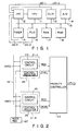
- Fig. 1 shows the entire structure of a 1-chip microcomputer including an interrupt control circuit according to the present invention.
- the 1-chip microcomputer comprises central processing unit (CPU) 11, interrupt control circuit (IRC) 12, serial input/output circuit (SI/O) 13, analog/digital converter (A/D) 14, timer 15, parallel input/output circuit (PI/O) 16, random access memory (RAM) 17, and read-only memory (ROM) 18, all of which are connected to one another through internal data bus 19.
- CPU central processing unit
- IRC interrupt control circuit
- SI/O serial input/output circuit
- A/D analog/digital converter
- PI/O parallel input/output circuit
- RAM random access memory
- ROM read-only memory
- interrupt request means which request interrupt for CPU 11.
- These interrupt request means output interrupt request signals, which are supplied to interrupt control circuit 12 through exclusive interrupt signal lines 20-1 to 20-4.
- interrupt control circuit 12 receives interrupt request signals, it determines the priority of the interrupt request signals in accordance with the predetermined priority of the interrupt requesting means and the priority level of the request signals output from each interrupt request means, and supplies the highest priority interrupt request signal to CPU 11.
- FIG. 2 shows interrupt control circuit (IRC) 12 shown in Fig. 1.
- Interrupt control circuit (IRC) 12 comprises four interrupt processing circuits 21-1 to 21-4 corresponding to the above-mentioned four interrupt request means, serial input/output circuit 13, analog/digital converter 14, timer 15, and parallel input/output circuit 18.
- Interrupt control circuit (IRC) 12 also comprises mode register 22 and priority controller 23 both of which are common to those interrupt processing circuits 21-1 to 21-4.
- Each of interrupt processing circuits 21-1 to 21-4 has control circuit 24 and control register 25.
- each interrupt processing circuit the interrupt request signal IREQ from an interrupt request means or the data supplied through internal data bus 19 is latched by an internal latch and subjected to a predetermined processing. Then, the processed data is output as an interrupt signal REQ to priority controller 23.
- Control register 25 stores data representing the interrupt priority levels of interrupt request signals from the interrupt request means, which is output as a level signal LEVEL to priority controller 23 together with the above-mentioned interrupt signal REQ.
- Priority controller 23 determines the priority of the interrupt request signals in accordance with the signals output from interrupt processing circuits 21-1 to 21-4, and transmits the highest priority interrupt request signal to CPU 11.
- Fig. 3 is a circuit diagram showing in detail the structure of the interrupt processing circuits 21-1 to 21-4. Since all of circuits 21-1 to 21-4 have the same structure, only circuit 21-1 will be described below.
- Internal data bus 19 transmits data constituted by a plurality of bits, and data of the least significant bit DB0 is supplied to the data input terminal (D) of 1-bit latch circuit 31.
- a write control signal WSTB is supplied to the control input terminal (G) of latch control circuit 31.
- An output signal of AND gate circuit 32 is supplied to the clear input terminal (C) of latch control circuit 31.
- Date MODE stored in mode register 22 is supplied to one of the two input terminals of AND gate circuit 32 via inverter 33, and a system reset signal RESET is supplied to the other input terminal thereof.
- the interrupt request signal IREQ output from the interrupt request means is supplied to the control terminal (G) of 1-bit latch circuit 34.
- the data input terminal (D) of latch circuit 34 is connected to the power source set at a "H" level.
- the output signal of three-inputs AND gate circuit 35 is supplied to the clear input terminal (C) of latch circuit 34.
- the above-mentioned data MODE is input to a first input terminal of AND gate circuit 35, the system reset signal RESET to a second input terminal, and the output signal of NAND gate circuit 36 to a third input terminal.
- Data of the least significant bit DB0 of internal data but 19 is supplied to one of the input terminals of NAND gate circuit 36 via inverter 37, and the write control signal WSTB is supplied to the other input terminals thereof.
- Signals output from the output terminals (Q) of latch circuits 31 and 34 are supplied in parallel to the input terminals of two-inputs OR gate circuit 38.
- An output signal of OR gate circuit 38 is supplied to the data input terminal (D) of timing set 1-bit latch circuit 39, and also to the least significant bit DB0 of internal data but 19 through transfer gate 40.
- a timing signal TMG is supplied from a timing signal generating circuit (not shown) to the control input terminal (G) of latch circuit 39.
- An output signal from the terminal (Q) of latch circuit 39 is supplied to one of the input terminals of AND gate circuit 41.
- 1-bit latch circuit 42 serves as a mask for masking an interrupt request signal.
- Data of the bit DB1, the bit immediately upper than the least significant bit DBO of internal data bus 19, is supplied to the data input terminal (D) of latch circuit 42.
- the mask signal MASK is supplied to the control input terminal (G) of latch circuit 42.
- An output signal from the output terminal ( Q ) of latch circuit 42 is supplied to the other input terminal of AND gate circuit 41.
- An output signal from the output terminal (Q) of latch circuit 42 is supplied to DB1 of internal data bus 19 via transfer gate 43.
- Transfer gates 40 and 43 are operated under control of a read control signal RSTB.
- the other interrupt processing circuits 21-2 to 21-4 have the same structure as the above-described circuit 21-1, except for the bit of the internal data bus.
- Fig. 4 shows the memory state of each of control registers 25 shown in Fig. 2.
- data of three interrupt priority levels is written in the control register.
- the signals RSTB and WSTB are respectively used to read/write data from/into control register 25. These signals are set by software executed by CPU 11 (Fig. 1).
- the data representing one of the three interrupt priority levels is supplied to priority controller 23, and utilized therein to determine the priority of the interrupt request signals.
- CPU 11 causes mode register 22 to store data through software processing. For example, "1" level data is stored in mode register 22 in a normal operation, and "0" level data in an inspection mode.
- a system reset signal RESET is set to a “0" level.
- the output signals of AND gate circuits 32 and 35 are also set to a “0” level, with the result that latch circuits 31 and 34 are reset. Thereafter, system reset signal RESET rises to a "1" level.
- mode data MODE of "0" level is stored in mode register 22 by software processing of CPU 11.
- the output of AND gate circuit 35 is set to "0" level and latch circuit 34 is set to the cleared state, while the output of AND gate circuit 32 is set to "1" level and latch circuit 31 is released from the reset state.
- Latch circuit 31 latches data of DB0 of internal data bus 19, and the output signal from the terminal (Q) is supplied through OR gate circuit 38 to latch circuit 39.
- a timing signal TMG is supplied from a timing signal generating circuit (not shown) to latch circuit 39, the output at the terminal (Q) of latch circuit 39 is set in response to the signal supplied to the data input terminal.
- AND gate circuit 41 outputs an interrupt request signal REQ to priority controller 23, in accordance with the level at the output terminal ( Q ) of latch circuit 42 in a masking state or a non-masking state.
- latch circuit 42 To set latch circuit 42 to a masking state, "1" level data is supplied to DB1 of internal data bus 19. and a signal WSTB is supplied to latch circuit 42, thereby setting the output terminal ( Q ) of latch circuit 42 to a "0" level.
- Output signals from terminals (Q) of latch circuits 31 and 34 can be output to DB0 of internal data bus 19, and an output signal from the output terminal (Q) of latch circuit 42 can be output to DB1.
- the data reading is performed in response to a read control signal RSTB.
- the present invention provides an interrupt control circuit for use in a 1-chip microcomputer having priority determining means which is easy to inspect.
Landscapes
- Engineering & Computer Science (AREA)
- Theoretical Computer Science (AREA)
- General Engineering & Computer Science (AREA)
- Physics & Mathematics (AREA)
- General Physics & Mathematics (AREA)
- Software Systems (AREA)
- Computer Hardware Design (AREA)
- Quality & Reliability (AREA)
- Microcomputers (AREA)
- Bus Control (AREA)
- Test And Diagnosis Of Digital Computers (AREA)
Abstract
Description
- This invention relates to an interrupt control circuit for use in a 1-chip microcomputer, and more particularly to an interrupt control circuit having priority determining means which is easy to inspect.
- An interrupt control circuit for use in a microcomputer or the like determines priority of a plurality of interrupt requests, and outputs to the CPU a request of the highest priority.
- The conventional interrupt control circuit has a plurality of interrupt request latches. Each of the latches is set in response to interrupt request signal sent from interrupt request means such as a serial or parallel input/output circuit, an A/D converter, a timer, or the like, and reset in response to an interrupt request clear signal.
- If the interrupt control circuit is an LSI circuit such as 1-chip microcomputer, an interrupt request signal can be input through a terminal of the microcomputer. In this case, in order to inspect the circuit, a desired inspection pattern is supplied from an external circuit, thereby setting each interrupt request latch to a desired state.
- In contrast, if the interrupt control circuit is incorporated in a 1-chip microcomputer, an interrupt request signal is directly input to the circuit from the input/output circuit also incorporated in the microcomputer, not from an external circuit. In this case, in order to set a specific interrupt request latch to a desired state, the input/output circuit connected to the interrupt request latch must be set to an appropriate state. This is a critical drawback in inspecting the priority determining means used in the interrupt control circuit in three respects. First, the interrupt control circuit cannot be inspected independently. Second, a great number of inspection patterns must be input to inspect many combinations of circuits, which may lengthen the inspecting time very much. Third, the inspection patterns required may be very complicated.
- The second and third drawbacks are prominent, especially when the input/output circuit has many functions, and a great number of interrupt request signals are therefore generated. The second and third drawbacks are also great, when the input/output circuit includes a timer, which outputs signals at regular intervals.
- As described above, the conventional interrupt control circuit for use in a 1-chip microcomputer is disadvantageous in that a long period of time is required for inspecting the priority determining function, and the inspecting operation is complicated.
- The present invention has been made in consideration of the above circumstances, and its object is to provide an interrupt control circuit for use in a 1-chip microcomputer having priority determining means which is easy to inspect.
- According to a first aspect of the present invention, there is provided an interrupt control circuit for use in a 1-chip microcomputer, comprising a CPU, a plurality of interrupt request means, each generating interrupt request signals to be supplied to the CPU, and interrupt control/priority determining means, connected to the CPU via an internal data bus, supplied with the interrupt request signals generated by the plurality of interrupt request means for determining the priority of the interrupt request signals and outputting the highest priority interrupt request signals to the CPU, and supplied with an interrupt request signal from the CPU through the internal data bus.
- According to a second aspect of the present invention, there is provided an interrupt control circuit for use in a 1-chip microcomputer, comprising a CPU, a plurality of interrupt request means, each generating interrupt request signals to be supplied to the CPU, mode data storing means for storing mode data for discriminating between a normal operation mode and an inspection mode, a plurality of interrupt request latching means for latching the interrupt request signals from the interrupt request means when the mode data storing means stores data corresponding to the normal operation mode, and latching data on the internal data bus as an interrupt request signal when the mode data storing means stores data corresponding to the inspection mode, and a priority determining means for determining the priority of the interrupt requests stored in the plurality of interrupt request holding means.
- This invention can be more fully understood from the following detailed description when taken in conjunction with the accompanying drawings, in which:
- Fig. 1 is a block diagram showing the entire structure of a 1-chip microcomputer including an interrupt control circuit according to the present invention;
- Fig. 2 is a block diagram showing the interrupt control circuit shown in Fig. 1;
- Fig. 3 is a circuit diagram showing a detailed structure of the control circuit of the interrupt control circuit shown in Fig. 2; and
- Fig. 4 shows the data memory state in the control register shown in Fig. 2.
- An embodiment of the present invention will be described below with reference to accompanying drawings.
- Fig. 1 shows the entire structure of a 1-chip microcomputer including an interrupt control circuit according to the present invention. As is illustrated in Fig. 1, the 1-chip microcomputer comprises central processing unit (CPU) 11, interrupt control circuit (IRC) 12, serial input/output circuit (SI/O) 13, analog/digital converter (A/D) 14,
timer 15, parallel input/output circuit (PI/O) 16, random access memory (RAM) 17, and read-only memory (ROM) 18, all of which are connected to one another throughinternal data bus 19. - Serial input/
output circuit 13, analog/digital converter 14,timer 15 and parallel input/output circuit 18 are interrupt request means which request interrupt forCPU 11. These interrupt request means output interrupt request signals, which are supplied to interruptcontrol circuit 12 through exclusive interrupt signal lines 20-1 to 20-4. Wheninterrupt control circuit 12 receives interrupt request signals, it determines the priority of the interrupt request signals in accordance with the predetermined priority of the interrupt requesting means and the priority level of the request signals output from each interrupt request means, and supplies the highest priority interrupt request signal toCPU 11. - Fig. 2 shows interrupt control circuit (IRC) 12 shown in Fig. 1. Interrupt control circuit (IRC) 12 comprises four interrupt processing circuits 21-1 to 21-4 corresponding to the above-mentioned four interrupt request means, serial input/
output circuit 13, analog/digital converter 14,timer 15, and parallel input/output circuit 18. Interrupt control circuit (IRC) 12 also comprisesmode register 22 andpriority controller 23 both of which are common to those interrupt processing circuits 21-1 to 21-4. Each of interrupt processing circuits 21-1 to 21-4 hascontrol circuit 24 andcontrol register 25. - An interrupt request signal IREQ output from one of the interrupt request means and transmitted through the exclusive signal line (20-1, 20-2, 20-3 or 20-4), data consisting of a plurality of bits transmitted through
internal data bus 19, and data stored inmode register 22 are supplied in parallel to each of interrupt processing circuits 21-1 to 21-4. - In each interrupt processing circuit, the interrupt request signal IREQ from an interrupt request means or the data supplied through
internal data bus 19 is latched by an internal latch and subjected to a predetermined processing. Then, the processed data is output as an interrupt signal REQ topriority controller 23.Control register 25 stores data representing the interrupt priority levels of interrupt request signals from the interrupt request means, which is output as a level signal LEVEL topriority controller 23 together with the above-mentioned interrupt signal REQ. -
Priority controller 23 determines the priority of the interrupt request signals in accordance with the signals output from interrupt processing circuits 21-1 to 21-4, and transmits the highest priority interrupt request signal toCPU 11. - Fig. 3 is a circuit diagram showing in detail the structure of the interrupt processing circuits 21-1 to 21-4. Since all of circuits 21-1 to 21-4 have the same structure, only circuit 21-1 will be described below.
Internal data bus 19 transmits data constituted by a plurality of bits, and data of the least significant bit DB0 is supplied to the data input terminal (D) of 1-bit latch circuit 31. A write control signal WSTB is supplied to the control input terminal (G) oflatch control circuit 31. An output signal ofAND gate circuit 32 is supplied to the clear input terminal (C) oflatch control circuit 31. Date MODE stored inmode register 22 is supplied to one of the two input terminals ofAND gate circuit 32 via inverter 33, and a system reset signalRESET is supplied to the other input terminal thereof. - The interrupt request signal IREQ output from the interrupt request means is supplied to the control terminal (G) of 1-
bit latch circuit 34. The data input terminal (D) oflatch circuit 34 is connected to the power source set at a "H" level. The output signal of three-inputs ANDgate circuit 35 is supplied to the clear input terminal (C) oflatch circuit 34. The above-mentioned data MODE is input to a first input terminal ofAND gate circuit 35, the system reset signalRESET to a second input terminal, and the output signal ofNAND gate circuit 36 to a third input terminal. Data of the least significant bit DB0 of internal data but 19 is supplied to one of the input terminals ofNAND gate circuit 36 viainverter 37, and the write control signal WSTB is supplied to the other input terminals thereof. - Signals output from the output terminals (Q) of
latch circuits gate circuit 38. An output signal ofOR gate circuit 38 is supplied to the data input terminal (D) of timing set 1-bit latch circuit 39, and also to the least significant bit DB0 of internal data but 19 throughtransfer gate 40. A timing signal TMG is supplied from a timing signal generating circuit (not shown) to the control input terminal (G) oflatch circuit 39. An output signal from the terminal (Q) oflatch circuit 39 is supplied to one of the input terminals ofAND gate circuit 41. - 1-
bit latch circuit 42 serves as a mask for masking an interrupt request signal. Data of the bit DB1, the bit immediately upper than the least significant bit DBO ofinternal data bus 19, is supplied to the data input terminal (D) oflatch circuit 42. The mask signal MASK is supplied to the control input terminal (G) oflatch circuit 42. An output signal from the output terminal (Q ) oflatch circuit 42 is supplied to the other input terminal ofAND gate circuit 41. An output signal from the output terminal (Q) oflatch circuit 42 is supplied to DB1 ofinternal data bus 19 viatransfer gate 43. -
Transfer gates - The other interrupt processing circuits 21-2 to 21-4 have the same structure as the above-described circuit 21-1, except for the bit of the internal data bus.
- Fig. 4 shows the memory state of each of
control registers 25 shown in Fig. 2. As illustrated in Fig. 4, data of three interrupt priority levels is written in the control register. The signals RSTB and WSTB are respectively used to read/write data from/intocontrol register 25. These signals are set by software executed by CPU 11 (Fig. 1). The data representing one of the three interrupt priority levels is supplied topriority controller 23, and utilized therein to determine the priority of the interrupt request signals. - The operation of the above-described interrupt control circuit will now be described.
-
CPU 11causes mode register 22 to store data through software processing. For example, "1" level data is stored inmode register 22 in a normal operation, and "0" level data in an inspection mode. A system reset signalRESET is set to a "0" level. At this time, the output signals of ANDgate circuits circuits RESET rises to a "1" level. - In a normal operation mode, when an interrupt request signal IREQ is input to any one of interrupt processing circuits 21-1 to 21-4, "1" level data is latched by
latch circuit 34 in the interrupt processing circuit, and the output at the terminal (Q) oflatch circuit 34 is of "1" level. As a result, the output ofOR gate circuit 38 becomes "1" level. Then, the timing signal generating circuit (not shown) outputs a timing signal TMG, and the output at the terminal (Q) oflatch lu circuit 39 becomes "1" level. At this time, if the output at the terminal (Q ) oflatch circuit 42 serving as a mask is of "1" level, i.e., iflatch circuit 42 is in a non-masking state, the output of ANDgate circuit 41 is also of "1" levels As a result, an interrupt request signal REQ is supplied topriority controller 23.Priority controller 23 determines the priority of interrupt request signals supplied from interrupt processing circuits 21-1 to 21-4, and supplies the highest priority interrupt request signal toCPU 11. The interrupt processing is thus executed. After the execution of an interrupt processing,CPU 11 outputs "0" level data to DB0 ofinternal data bus 19, and supplies write control signal WSTB to controlregister 25. As a result, the output ofinverter 37 is of "0" level, and the output ofNAND gate circuit 36 is of "0" level, and the output of ANDgate circuit 35 is accordingly of "0" level. Thus,latch circuit 34 is reset. - In an inspection mode, mode data MODE of "0" level is stored in
mode register 22 by software processing ofCPU 11. At this time, the output of ANDgate circuit 35 is set to "0" level andlatch circuit 34 is set to the cleared state, while the output of ANDgate circuit 32 is set to "1" level andlatch circuit 31 is released from the reset state.Latch circuit 31 latches data of DB0 ofinternal data bus 19, and the output signal from the terminal (Q) is supplied throughOR gate circuit 38 to latchcircuit 39. Then, when a timing signal TMG is supplied from a timing signal generating circuit (not shown) to latchcircuit 39, the output at the terminal (Q) oflatch circuit 39 is set in response to the signal supplied to the data input terminal. Thereafter, in the same manner as in the normal operation mode, ANDgate circuit 41 outputs an interrupt request signal REQ topriority controller 23, in accordance with the level at the output terminal (Q ) oflatch circuit 42 in a masking state or a non-masking state. - To set
latch circuit 42 to a masking state, "1" level data is supplied to DB1 ofinternal data bus 19. and a signal WSTB is supplied to latchcircuit 42, thereby setting the output terminal (Q ) oflatch circuit 42 to a "0" level. Output signals from terminals (Q) oflatch circuits internal data bus 19, and an output signal from the output terminal (Q) oflatch circuit 42 can be output to DB1. The data reading is performed in response to a read control signal RSTB. More specifically, when a read control signal RSTB of "1" level is supplied to the interrupt processing circuit, bothtransfer gates latch circuit internal data bus 19, and an output signal from the terminal Q oflatch circuit 42 to DBI thereof. In this embodiment, level set operation of interrupt request is executed by software ofCPU 11. - In a conventional interrupt control circuit in which seven interrupt priority levels are stored in the control register and the number of the interrupt request means are 30, an inspecting pattern of 150,000 steps was required to inspect the priority controller. According to the present invention, under the same conditions, the number of the steps of the inspection pattern is 15,000, i.e. 1/10 of that in the conventional apparatus. Hence, it takes 1/10 shorter period of time to inspect the interrupt control circuit, and also to form the inspecting pattern in comparison with the case of the conventional circuit. Thus, the inspection of the interrupt control circuit can be performed very much easily.
- As has been described above, the present invention provides an interrupt control circuit for use in a 1-chip microcomputer having priority determining means which is easy to inspect.
- Reference signs in the claims are intended for better understanding and shall not limit the scope.
Claims (14)
a CPU (11);
a plurality of interrupt request means (13, 14, 15, 16), each generating interrupt request signals to be supplied to the CPU; and
interrupt control/priority determining means (12), connected to said CPU (11) via an internal data bus (19), supplied with the interrupt request signals generated by said interrupt request means (13, 14, 15, 16), for determining the priority of the interrupt request signals and outputting the highest priority interrupt request signals to said CPU (11), and supplied with an interrupt request signal from said CPU (11) via said internal data bus (19).
a CPU (11);
a plurality of interrupt request means (13, 14, 15, 16), each generating interrupt request signals to be supplied to said CPU (11);
a mode data storing means (22) for storing mode data for discriminating between a normal operation mode and an inspection mode;
a plurality of first interrupt request latching means (34), each latching the interrupt request signals from each of the interrupt request means, when the mode data storing means (22) stores data corresponding to the normal operation mode;
a plurality of second interrupt request latching means (31), each latching data supplied from the CPU (11) through the internal data bus (19) as an interrupt request signal, when the mode data storing means (22) stores data corresponding to the inspection mode; and a priority determining means (23) for determining the priority of the interrupt request signals stored in said first and second interrupt request latching means (34, 31).
a plurality of data latching means (42) for latching the data supplied from said CPU (11) through said internal data bus (19) as mask data; and
a plurality of control gates (41) for supplying to said priority determining means the content of said data latching means (34) or of said second interrupt request latching means (31) in accordance with the mask data latched in said fourth interrupt request latching means.
Applications Claiming Priority (2)
| Application Number | Priority Date | Filing Date | Title |
|---|---|---|---|
| JP234956/89 | 1989-09-11 | ||
| JP1234956A JPH0397036A (en) | 1989-09-11 | 1989-09-11 | Interrupt control circuit |
Publications (2)
| Publication Number | Publication Date |
|---|---|
| EP0417748A2 true EP0417748A2 (en) | 1991-03-20 |
| EP0417748A3 EP0417748A3 (en) | 1992-01-08 |
Family
ID=16978894
Family Applications (1)
| Application Number | Title | Priority Date | Filing Date |
|---|---|---|---|
| EP19900117524 Withdrawn EP0417748A3 (en) | 1989-09-11 | 1990-09-11 | Interrupt control circuit for use in 1-chip microcomputer |
Country Status (3)
| Country | Link |
|---|---|
| EP (1) | EP0417748A3 (en) |
| JP (1) | JPH0397036A (en) |
| KR (1) | KR930005771B1 (en) |
Cited By (4)
| Publication number | Priority date | Publication date | Assignee | Title |
|---|---|---|---|---|
| EP0619899A4 (en) * | 1992-01-02 | 1994-09-02 | Amdahl Corp | Software control of hardware interruptions. |
| WO1997044734A1 (en) * | 1996-05-17 | 1997-11-27 | Advanced Micro Devices, Inc. | System and method for testing and debugging a multiprocessing interrupt controller |
| CN111552599A (en) * | 2020-04-26 | 2020-08-18 | 武汉精测电子集团股份有限公司 | Distributed process processing system, semiconductor aging test method and system and distributed system |
| CN114860630A (en) * | 2022-04-27 | 2022-08-05 | 深圳市洛仑兹技术有限公司 | Digital processing circuit and signal processing method |
Families Citing this family (2)
| Publication number | Priority date | Publication date | Assignee | Title |
|---|---|---|---|---|
| KR100393765B1 (en) * | 1996-03-26 | 2004-03-10 | 엘지전자 주식회사 | Device for controlling interrupt |
| KR100575608B1 (en) * | 1998-10-09 | 2006-09-28 | 매그나칩 반도체 유한회사 | Bus control circuit |
Family Cites Families (2)
| Publication number | Priority date | Publication date | Assignee | Title |
|---|---|---|---|---|
| JPS5232236A (en) * | 1975-09-05 | 1977-03-11 | Toshiba Corp | Testing device for interrupt processing circuit |
| JPS52156528A (en) * | 1976-06-22 | 1977-12-27 | Mitsubishi Electric Corp | Micro-processor interruption controller |
-
1989
- 1989-09-11 JP JP1234956A patent/JPH0397036A/en active Pending
-
1990
- 1990-09-11 KR KR1019900014301A patent/KR930005771B1/en not_active Expired - Fee Related
- 1990-09-11 EP EP19900117524 patent/EP0417748A3/en not_active Withdrawn
Cited By (6)
| Publication number | Priority date | Publication date | Assignee | Title |
|---|---|---|---|---|
| EP0619899A4 (en) * | 1992-01-02 | 1994-09-02 | Amdahl Corp | Software control of hardware interruptions. |
| WO1997044734A1 (en) * | 1996-05-17 | 1997-11-27 | Advanced Micro Devices, Inc. | System and method for testing and debugging a multiprocessing interrupt controller |
| CN111552599A (en) * | 2020-04-26 | 2020-08-18 | 武汉精测电子集团股份有限公司 | Distributed process processing system, semiconductor aging test method and system and distributed system |
| CN111552599B (en) * | 2020-04-26 | 2024-04-09 | 武汉精测电子集团股份有限公司 | Distributed process processing system, semiconductor aging test method and system and distributed system |
| CN114860630A (en) * | 2022-04-27 | 2022-08-05 | 深圳市洛仑兹技术有限公司 | Digital processing circuit and signal processing method |
| CN114860630B (en) * | 2022-04-27 | 2023-04-18 | 深圳市洛仑兹技术有限公司 | Digital processing circuit and signal processing method |
Also Published As
| Publication number | Publication date |
|---|---|
| EP0417748A3 (en) | 1992-01-08 |
| JPH0397036A (en) | 1991-04-23 |
| KR930005771B1 (en) | 1993-06-24 |
| KR910006855A (en) | 1991-04-30 |
Similar Documents
| Publication | Publication Date | Title |
|---|---|---|
| US4271466A (en) | Direct memory access control system with byte/word control of data bus | |
| US4716526A (en) | Multiprocessor system | |
| US5093780A (en) | Inter-processor transmission system having data link which automatically and periodically reads and writes the transfer data | |
| US6192442B1 (en) | Interrupt controller | |
| US4467420A (en) | One-chip microcomputer | |
| US5416919A (en) | Semiconductor integrated circuit with functional blocks capable of being individually tested externally | |
| KR890015143A (en) | Direct Memory Access Control | |
| EP0408353B1 (en) | Semiconductor integrated circuit | |
| EP0417748A2 (en) | Interrupt control circuit for use in 1-chip microcomputer | |
| US4628448A (en) | Operation mode setting apparatus on a single chip microprocessor | |
| US5159263A (en) | Lsi system having a test facilitating circuit | |
| EP0331487B1 (en) | Data transfer control system | |
| EP0167140A2 (en) | Interruption control circuit | |
| US6874049B1 (en) | Semaphores with interrupt mechanism | |
| US5341380A (en) | Large-scale integrated circuit device | |
| JPS6361697B2 (en) | ||
| JP2571090B2 (en) | Address transmitting device and receiving device | |
| JPS6491235A (en) | Control system for counter circuit | |
| JP2575895B2 (en) | Control signal switching device for integrated circuits | |
| EP0098170B1 (en) | Access control processing system in computer system | |
| KR940001271B1 (en) | PC Interrupt System | |
| JPS622344A (en) | information transmission device | |
| JP2814849B2 (en) | Communication control device | |
| KR920009452B1 (en) | Data electrical transmission circuit | |
| JPS60117847A (en) | Data control circuit |
Legal Events
| Date | Code | Title | Description |
|---|---|---|---|
| PUAI | Public reference made under article 153(3) epc to a published international application that has entered the european phase |
Free format text: ORIGINAL CODE: 0009012 |
|
| 17P | Request for examination filed |
Effective date: 19900911 |
|
| AK | Designated contracting states |
Kind code of ref document: A2 Designated state(s): DE FR GB |
|
| PUAL | Search report despatched |
Free format text: ORIGINAL CODE: 0009013 |
|
| AK | Designated contracting states |
Kind code of ref document: A3 Designated state(s): DE FR GB |
|
| 17Q | First examination report despatched |
Effective date: 19940803 |
|
| STAA | Information on the status of an ep patent application or granted ep patent |
Free format text: STATUS: THE APPLICATION IS DEEMED TO BE WITHDRAWN |
|
| 18D | Application deemed to be withdrawn |
Effective date: 19941214 |