EP0413614A2 - Electrical connections and a method for making the same - Google Patents
Electrical connections and a method for making the same Download PDFInfo
- Publication number
- EP0413614A2 EP0413614A2 EP90309108A EP90309108A EP0413614A2 EP 0413614 A2 EP0413614 A2 EP 0413614A2 EP 90309108 A EP90309108 A EP 90309108A EP 90309108 A EP90309108 A EP 90309108A EP 0413614 A2 EP0413614 A2 EP 0413614A2
- Authority
- EP
- European Patent Office
- Prior art keywords
- particles
- adhesive
- electrode
- substrate
- light
- Prior art date
- Legal status (The legal status is an assumption and is not a legal conclusion. Google has not performed a legal analysis and makes no representation as to the accuracy of the status listed.)
- Withdrawn
Links
Images

Classifications
-
- H—ELECTRICITY
- H01—ELECTRIC ELEMENTS
- H01R—ELECTRICALLY-CONDUCTIVE CONNECTIONS; STRUCTURAL ASSOCIATIONS OF A PLURALITY OF MUTUALLY-INSULATED ELECTRICAL CONNECTING ELEMENTS; COUPLING DEVICES; CURRENT COLLECTORS
- H01R12/00—Structural associations of a plurality of mutually-insulated electrical connecting elements, specially adapted for printed circuits, e.g. printed circuit boards [PCB], flat or ribbon cables, or like generally planar structures, e.g. terminal strips, terminal blocks; Coupling devices specially adapted for printed circuits, flat or ribbon cables, or like generally planar structures; Terminals specially adapted for contact with, or insertion into, printed circuits, flat or ribbon cables, or like generally planar structures
- H01R12/50—Fixed connections
- H01R12/59—Fixed connections for flexible printed circuits, flat or ribbon cables or like structures
- H01R12/62—Fixed connections for flexible printed circuits, flat or ribbon cables or like structures connecting to rigid printed circuits or like structures
-
- H—ELECTRICITY
- H01—ELECTRIC ELEMENTS
- H01R—ELECTRICALLY-CONDUCTIVE CONNECTIONS; STRUCTURAL ASSOCIATIONS OF A PLURALITY OF MUTUALLY-INSULATED ELECTRICAL CONNECTING ELEMENTS; COUPLING DEVICES; CURRENT COLLECTORS
- H01R4/00—Electrically-conductive connections between two or more conductive members in direct contact, i.e. touching one another; Means for effecting or maintaining such contact; Electrically-conductive connections having two or more spaced connecting locations for conductors and using contact members penetrating insulation
- H01R4/04—Electrically-conductive connections between two or more conductive members in direct contact, i.e. touching one another; Means for effecting or maintaining such contact; Electrically-conductive connections having two or more spaced connecting locations for conductors and using contact members penetrating insulation using electrically conductive adhesives
-
- H—ELECTRICITY
- H05—ELECTRIC TECHNIQUES NOT OTHERWISE PROVIDED FOR
- H05K—PRINTED CIRCUITS; CASINGS OR CONSTRUCTIONAL DETAILS OF ELECTRIC APPARATUS; MANUFACTURE OF ASSEMBLAGES OF ELECTRICAL COMPONENTS
- H05K3/00—Apparatus or processes for manufacturing printed circuits
- H05K3/30—Assembling printed circuits with electric components, e.g. with resistor
- H05K3/32—Assembling printed circuits with electric components, e.g. with resistor electrically connecting electric components or wires to printed circuits
- H05K3/321—Assembling printed circuits with electric components, e.g. with resistor electrically connecting electric components or wires to printed circuits by conductive adhesives
- H05K3/323—Assembling printed circuits with electric components, e.g. with resistor electrically connecting electric components or wires to printed circuits by conductive adhesives by applying an anisotropic conductive adhesive layer over an array of pads
-
- H—ELECTRICITY
- H05—ELECTRIC TECHNIQUES NOT OTHERWISE PROVIDED FOR
- H05K—PRINTED CIRCUITS; CASINGS OR CONSTRUCTIONAL DETAILS OF ELECTRIC APPARATUS; MANUFACTURE OF ASSEMBLAGES OF ELECTRICAL COMPONENTS
- H05K2201/00—Indexing scheme relating to printed circuits covered by H05K1/00
- H05K2201/01—Dielectrics
- H05K2201/0104—Properties and characteristics in general
- H05K2201/0108—Transparent
-
- H—ELECTRICITY
- H05—ELECTRIC TECHNIQUES NOT OTHERWISE PROVIDED FOR
- H05K—PRINTED CIRCUITS; CASINGS OR CONSTRUCTIONAL DETAILS OF ELECTRIC APPARATUS; MANUFACTURE OF ASSEMBLAGES OF ELECTRICAL COMPONENTS
- H05K2201/00—Indexing scheme relating to printed circuits covered by H05K1/00
- H05K2201/02—Fillers; Particles; Fibers; Reinforcement materials
- H05K2201/0203—Fillers and particles
- H05K2201/0206—Materials
- H05K2201/0221—Insulating particles having an electrically conductive coating
-
- H—ELECTRICITY
- H05—ELECTRIC TECHNIQUES NOT OTHERWISE PROVIDED FOR
- H05K—PRINTED CIRCUITS; CASINGS OR CONSTRUCTIONAL DETAILS OF ELECTRIC APPARATUS; MANUFACTURE OF ASSEMBLAGES OF ELECTRICAL COMPONENTS
- H05K2201/00—Indexing scheme relating to printed circuits covered by H05K1/00
- H05K2201/02—Fillers; Particles; Fibers; Reinforcement materials
- H05K2201/0203—Fillers and particles
- H05K2201/0206—Materials
- H05K2201/023—Hard particles, i.e. particles in conductive adhesive at least partly penetrating an electrode
-
- H—ELECTRICITY
- H05—ELECTRIC TECHNIQUES NOT OTHERWISE PROVIDED FOR
- H05K—PRINTED CIRCUITS; CASINGS OR CONSTRUCTIONAL DETAILS OF ELECTRIC APPARATUS; MANUFACTURE OF ASSEMBLAGES OF ELECTRICAL COMPONENTS
- H05K2201/00—Indexing scheme relating to printed circuits covered by H05K1/00
- H05K2201/02—Fillers; Particles; Fibers; Reinforcement materials
- H05K2201/0203—Fillers and particles
- H05K2201/0206—Materials
- H05K2201/0233—Deformable particles
-
- H—ELECTRICITY
- H05—ELECTRIC TECHNIQUES NOT OTHERWISE PROVIDED FOR
- H05K—PRINTED CIRCUITS; CASINGS OR CONSTRUCTIONAL DETAILS OF ELECTRIC APPARATUS; MANUFACTURE OF ASSEMBLAGES OF ELECTRICAL COMPONENTS
- H05K2201/00—Indexing scheme relating to printed circuits covered by H05K1/00
- H05K2201/02—Fillers; Particles; Fibers; Reinforcement materials
- H05K2201/0203—Fillers and particles
- H05K2201/0263—Details about a collection of particles
- H05K2201/0272—Mixed conductive particles, i.e. using different conductive particles, e.g. differing in shape
-
- H—ELECTRICITY
- H05—ELECTRIC TECHNIQUES NOT OTHERWISE PROVIDED FOR
- H05K—PRINTED CIRCUITS; CASINGS OR CONSTRUCTIONAL DETAILS OF ELECTRIC APPARATUS; MANUFACTURE OF ASSEMBLAGES OF ELECTRICAL COMPONENTS
- H05K2201/00—Indexing scheme relating to printed circuits covered by H05K1/00
- H05K2201/20—Details of printed circuits not provided for in H05K2201/01 - H05K2201/10
- H05K2201/2036—Permanent spacer or stand-off in a printed circuit or printed circuit assembly
-
- H—ELECTRICITY
- H05—ELECTRIC TECHNIQUES NOT OTHERWISE PROVIDED FOR
- H05K—PRINTED CIRCUITS; CASINGS OR CONSTRUCTIONAL DETAILS OF ELECTRIC APPARATUS; MANUFACTURE OF ASSEMBLAGES OF ELECTRICAL COMPONENTS
- H05K3/00—Apparatus or processes for manufacturing printed circuits
- H05K3/36—Assembling printed circuits with other printed circuits
- H05K3/361—Assembling flexible printed circuits with other printed circuits
Definitions
- the present invention relates to an improved electrical connection and a method for making the same.
- a substrate 7a is provided with an electrode arrangement 8a which consists of a number of electrode strips which are required to make electrical connection with corresponding electrode strips 8b provided on another substrate 7b.
- An FPC 9 comprises a flexible sheet made from polyimide and carrying a number of conductive strips 10 corresponding to the strips of the substrates 7a and 7b. The coupling together of the strips 10, 8a and 8b of the flexible sheet and the substrates is made through anisotropic conductive films 11.
- connection since the connection is made through an FPC, there are two coupling sites which require much care and processing as compared with the case of a single site connection. The possibility of connection error is also doubled.
- the FPC is adhered to the substrates at a high temperature and under pressure. The flexible sheet is thermally expanded during the thermal treatment, and consequently the alignment of the conductive strips 10 with the corresponding strips 8a and 8b of the substrates is often sheared, resulting in disconnections or connection errors.
- the FPC sometimes separates from the substrates when external force is applied just after the connection is completed.
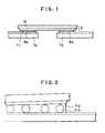
- Fig. 2 of the accompanying drawings is an explanatory view showing the structure of the conventional anisotropic conductive film and it will be seen that the film is comprised of a sheet 11a of adhesive in which a large number of conductive particles 11b are uniformly dispersed. Because the conductive particles are non-deformable, the electrodes 10 and 8a are easily disconnected from the particles as a consequence of thermal expansion or contraction with environmental temperature changes.
- connection system which inter alia will increase the yield of electrical connections made between electrode strips formed on substrates.
- electrodes on a first substrate are placed over and aligned with counterpart electrodes on a second substrate with a UV-light-curable electrically conductive adhesive between them and the first and second substrates are pressed against each other and exposed to UV light in order to harden the adhesive.
- the UV-light-curable adhesive has first and second kinds of particles dispersed therein, the first kind of particles being electrically conductive and preferably resilient and functioning to form current paths between the electrodes of the first and second substrates, and the second kind of particles functioning to protect the first kind of particles against excessive deformation.
- the first kind of particles comprise fine spheres or beads of synthetic resin material, such as polystyrene, which are coated with a film of conductive metal, for example gold.
- the second kind of particles are slightly smaller than the first kind of particles and may be made from any material which has sufficient hardness properties and is not easily crushed, for example Si02.
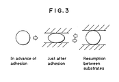
- Fig. 3 of the accompanying drawings illustrates the action of the first kind of particles in the making of an electrical connection according to the teachings of the present invention.
- the particles are formed so as to be resilient.
- the first kind of particles maintain their 100% diameter in advance of the application of pressure.
- the diameter is decreased to 60-95% of the original value when the pair of substrates are joined under pressure.
- the electrical contact between the first kind of particles and the electrodes of the substrates is ensured at least for as long as any relative deformation of the substrates does not exceed 100%-(60-95%) of the diameter because of the resilience of the particles. This is made certain furthermore by making use of light instead of heat to harden the adhesive carrying the first and second particles. Other shortcomings arising from the high temperature arising during heat treatment are also removed.
- a glass substrate 1 is formed with a number of parallel conductive strips 3a made from a transparent conductive material such as indium tin oxide (ITO), and a printed circuit board 2 is provided with a number of parallel conductive strips 3b made of copper corresponding to the strips 3a of the glass substrate 1.
- the glass substrate 1 is used for example for forming a liquid crystal display by sandwiching a liquid crystal layer between it and a similar counterpart substrate.
- the circuit formed on the board 2 is provided to supply drive signals to the strips 3a and 3b.
- Fig. 5 shows the connection between the strips 3a and 3b.
- a UV-light-curable electrically insulating adhesive 4 in which a number of fine particles 5 of a first kind and fine particles 6 of a second kind are dispersed.
- the diameter of the first kind of particles 5 is slightly larger than that of the second kind of particles 6.
- the adhesive 4 is exposed to UV light with the board 2 being pressed against the substrate 1, and the first kind of particles are deformed under this pressure until the distance between the board and the substrate decreases to the diameter of the second kind of particles.
- the second kind of particles thus protect the first kind of particles from being too much deformed.
- the first kind of particles have to make electrically conductive paths between the strips 3a and 3b, they are made from a conductive material such as a metal.
- Preferred resilient particles can be provided as the first kind of particles by coating a metallic film such as Au film on fine spheres of organic resin such as polystyrene.
- the second kind of particles can be made from any material as long as they are sufficiently hard and are not easily crushed by the pressure that is applied during the curing process.
- a 1200 angstroms thick ITO film was coated on a first 1.1 mm thick soda lime glass substrate by sputtering.
- the sheet resistance of the ITO film was measured to be 25 ⁇ .
- the ITO film was then patterned into 640 parallel strips of 175 ⁇ m width and 30 mm length by a known photolighographic process. The distance between adjacent strips was 350 ⁇ m. (The interval was 175 ⁇ m).
- the strips were designed to be extensions of electrodes defining pixels for a liquid crystal display.
- a 1000 angstroms thick ITO film was coated on a second 1.1 mm thick soda lime glass substrate by EB evaporation.
- the ITO film was then severed into 640 parallel strips of 175 ⁇ m width and 30 mm length by a known photolithographic process. The distance between adjacent strips was 350 um corresponding to those of the first substrate.
- the strips were designed to be connected to driving circuits for the liquid crystal display including ICs.
- a 5500 angstroms thick Ni film was formed on the ITO strips by plating. The 500 angstroms thickness of the Ni film was then replaced by a 500 angstroms thick Au film also by plating.
- the first substrate was placed over the second substrate with a UV-light-curable resin in which first and second kinds of particles were dispersed, the resin having been coated on the first or second substrate in advance by a dispenser. Care was taken to align the strips of the first substrate exactly with the corresponding strips of the second substrate.
- the first kind of particles were prepared by coating polystyrene particles of 7.5 ⁇ m diameter film 1000 angstroms thick Au films.
- the second kind of particles were Si02 particles of 5.0 ⁇ m diameter.
- the ratio by weight of resin to the first and second kinds of particles was chosen to be 107:14:4.
- the first and second substrates were then pressed against each other under 2.4 Kg/cm2 and exposed to UV light in order to harden the resin.
- connection resistance per strip was 0.5 ⁇ .
- insulation resistance between adjacent strips was 2.8 x 10⁹ ⁇ .
- a 1200 angstroms thick ITO film was coated on a first 1.1 mm thick soda lime glass substrate 14 by sputtering.
- the sheet resistance of the ITO film was measured to be 25 ⁇ .
- the ITO film was then patterned into a number of parallel strips of 175 ⁇ m width and 30 mm length by a known photolithographic process. The number of the strips was 640. The distance between adjacent strips was 350 ⁇ m. (The interval was 175 ⁇ m). the strips were designed to be extensions of electrodes defining pixels for a liquid crystal display.
- OLBs Outer Lead Bonding
- TABs Tepe Automated Bonding
- 80 parallel electrode strips 18 of 175 ⁇ m width and 30 mm length were formed in each OLB. These electrodes were of copper film of 0.035 mm thickness.
- the other end of each TAB terminated in an ILB (Inner Lead Bonding).
- the substrates 17 of the TAB were made from a Kapton film of 0.125 mm thickness manufactured by Dupont.
- the second substrates 16 were placed over the first substrate 14 with a UV-light-curable resin 4 in which first and second kinds of particles were dispersed therebetween. In so doing, care was taken to align the strips of the first substrate exactly with the corresponding strips of the second substrates.
- the first kind of particles were prepared by coating polystyrene particles of 7.5 ⁇ m diameter with 1000 angstroms thick Au films.
- the second particles were Si02 spheres of 5.0 ⁇ m diameter.
- the ratio by weight of the resin to the first and second kinds of particles was chosen to be 107:14:4.
- the first and second substrates were then pressed against each other under 2.4 Kg/cm2 and exposed to UV light in order to harden the resin in the same manner as in the first example.
- connection resistance per strip was 0.5 ⁇ .
- insulation resistance between adjacent strips was 2.8 x 10⁹ ⁇ .
- Example 2 This example was conducted in substantially the same manner as for Example 1 except that the second substrate was different.
- Two printed circuit boards were used as the second substrates.
- Each board was made of a 1.1 mm thick glass epoxy substrate on which 320 parallel electrodes of 175 m width and 30 mm length were formed and connected with circuits formed on the same board.
- the electrodes were of copper film of 0.125 mm thickness.
- the other processes were the same as those of Example 1 and will not be repeated.
- connection resistance per strip was 0.5 ⁇ .
- insulation resistance between adjacent strips was 2.8 x 10⁹ ⁇ .
Abstract
Description
- The present invention relates to an improved electrical connection and a method for making the same.
- The electrical connections between substrates carrying electrode arrangements have commonly been made by means of FPC's (Flexible Printed Circuits) and such a connection is illustrated in Fig. 1 of the accompanying drawings. A
substrate 7a is provided with anelectrode arrangement 8a which consists of a number of electrode strips which are required to make electrical connection withcorresponding electrode strips 8b provided on anothersubstrate 7b. An FPC 9 comprises a flexible sheet made from polyimide and carrying a number ofconductive strips 10 corresponding to the strips of thesubstrates strips conductive films 11. - This method of making electrical connection gives rise to the following shortcomings. First, since the connection is made through an FPC, there are two coupling sites which require much care and processing as compared with the case of a single site connection. The possibility of connection error is also doubled. Second, the FPC is adhered to the substrates at a high temperature and under pressure. The flexible sheet is thermally expanded during the thermal treatment, and consequently the alignment of the
conductive strips 10 with thecorresponding strips - These disadvantages are considered to originate from the structure of the anisotropic conductive film. Fig. 2 of the accompanying drawings is an explanatory view showing the structure of the conventional anisotropic conductive film and it will be seen that the film is comprised of a sheet 11a of adhesive in which a large number of conductive particles 11b are uniformly dispersed. Because the conductive particles are non-deformable, the
electrodes - It is thus an object of the present invention to provide an improved connection system which inter alia will increase the yield of electrical connections made between electrode strips formed on substrates.
- In accordance with the present invention, electrodes on a first substrate are placed over and aligned with counterpart electrodes on a second substrate with a UV-light-curable electrically conductive adhesive between them and the first and second substrates are pressed against each other and exposed to UV light in order to harden the adhesive. The UV-light-curable adhesive has first and second kinds of particles dispersed therein, the first kind of particles being electrically conductive and preferably resilient and functioning to form current paths between the electrodes of the first and second substrates, and the second kind of particles functioning to protect the first kind of particles against excessive deformation.
- In an exemplary embodiment of the present invention which is described in detail hereinafter, the first kind of particles comprise fine spheres or beads of synthetic resin material, such as polystyrene, which are coated with a film of conductive metal, for example gold. The second kind of particles are slightly smaller than the first kind of particles and may be made from any material which has sufficient hardness properties and is not easily crushed, for example Si0₂.
- Fig. 3 of the accompanying drawings illustrates the action of the first kind of particles in the making of an electrical connection according to the teachings of the present invention. In this illustration the particles are formed so as to be resilient.
- As illustrated in Fig. 3, the first kind of particles maintain their 100% diameter in advance of the application of pressure. The diameter is decreased to 60-95% of the original value when the pair of substrates are joined under pressure. The electrical contact between the first kind of particles and the electrodes of the substrates, however, is ensured at least for as long as any relative deformation of the substrates does not exceed 100%-(60-95%) of the diameter because of the resilience of the particles. This is made certain furthermore by making use of light instead of heat to harden the adhesive carrying the first and second particles. Other shortcomings arising from the high temperature arising during heat treatment are also removed.
- The foregoing and further features of the present invention are set forth with particularity in the appended claims and will be well understood by those possessed of the relevant skills from consideration of the following detailed description of exemplary embodiments of the invention given with reference to the accompanying drawings.
-
- Fig. 1 is a side view showing a prior art FPC connection;
- Fig. 2 is an expanded partial view of the prior art connection of Fig. 1,
- Fig. 3 is an explanatory view showing the action of conductive particles in the making of an electrical connection in accordance with the teachings of the present invention;
- Figs. 4 and 5 are perspective and expanded partial cross-sectional views showing electrical connections in accordance with an embodiment of the present invention;
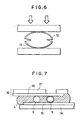
- Fig. 6 shows the destruction of particles of the first kind under excessive pressure; and
- Fig. 7 is an expanded cross-sectional view showing an electrical connection in accordance with another embodiment of the present invention.
- Referring now to Figs. 4 and 5, which illustrate a preferred embodiment of the invention, a glass substrate 1 is formed with a number of parallel
conductive strips 3a made from a transparent conductive material such as indium tin oxide (ITO), and a printedcircuit board 2 is provided with a number of parallelconductive strips 3b made of copper corresponding to thestrips 3a of the glass substrate 1. The glass substrate 1 is used for example for forming a liquid crystal display by sandwiching a liquid crystal layer between it and a similar counterpart substrate. The circuit formed on theboard 2 is provided to supply drive signals to thestrips - Fig. 5 shows the connection between the
strips board 2 and the substrate 1 is a UV-light-curable electrically insulatingadhesive 4 in which a number offine particles 5 of a first kind andfine particles 6 of a second kind are dispersed. The diameter of the first kind ofparticles 5 is slightly larger than that of the second kind ofparticles 6. Theadhesive 4 is exposed to UV light with theboard 2 being pressed against the substrate 1, and the first kind of particles are deformed under this pressure until the distance between the board and the substrate decreases to the diameter of the second kind of particles. The second kind of particles thus protect the first kind of particles from being too much deformed. - Since the first kind of particles have to make electrically conductive paths between the
strips - For comparative reference, when electrical connections were made between electrodes on a glass substrate and a printed board as illustrated in Fig. 5 but without the use of the second kind of particles, many of the
polystyrene particles 13 coated withAu films 12 which were used as the first kind of particles were crushed by the pressure applied during the curing process, as is illustrated in Fig. 6, so that disconnections happened. It is not necessarily impossible to adjust the pressure in order not to break the first kind of particles even without provision of the second kind of particles, but such adjustment is very difficult and is not practical. The second kind of particles are thus indispensable. The polystyrene particles coated with Au films can be deformed without destruction to 60% of their diameter, which fact was confirmed by experiment. The diameter of the second kind of particles, therefore, is chosen to be from 60% to 95% of that of the first kind of particles. - In the following, detailed explanations will be provided of the fabrication of several electrical connections in accordance with the teachings of the present invention and of tests that were conducted on the resulting connections.
- A 1200 angstroms thick ITO film was coated on a first 1.1 mm thick soda lime glass substrate by sputtering. The sheet resistance of the ITO film was measured to be 25Ω. The ITO film was then patterned into 640 parallel strips of 175 µm width and 30 mm length by a known photolighographic process. The distance between adjacent strips was 350 µm. (The interval was 175 µm). The strips were designed to be extensions of electrodes defining pixels for a liquid crystal display.
- A 1000 angstroms thick ITO film was coated on a second 1.1 mm thick soda lime glass substrate by EB evaporation. The ITO film was then severed into 640 parallel strips of 175 µm width and 30 mm length by a known photolithographic process. The distance between adjacent strips was 350 um corresponding to those of the first substrate. The strips were designed to be connected to driving circuits for the liquid crystal display including ICs. A 5500 angstroms thick Ni film was formed on the ITO strips by plating. The 500 angstroms thickness of the Ni film was then replaced by a 500 angstroms thick Au film also by plating.
- The first substrate was placed over the second substrate with a UV-light-curable resin in which first and second kinds of particles were dispersed, the resin having been coated on the first or second substrate in advance by a dispenser. Care was taken to align the strips of the first substrate exactly with the corresponding strips of the second substrate. The first kind of particles were prepared by coating polystyrene particles of 7.5 µm diameter film 1000 angstroms thick Au films. The second kind of particles were Si0₂ particles of 5.0 µm diameter. The ratio by weight of resin to the first and second kinds of particles was chosen to be 107:14:4. The first and second substrates were then pressed against each other under 2.4 Kg/cm² and exposed to UV light in order to harden the resin.
- As a result, the two sets of electrode strips were electrically coupled. The connection resistance per strip was 0.5 Ω. The insulation resistance between adjacent strips was 2.8 x 10⁹Ω. When thermal shock was repeatedly applied 100 times by varying the temperature between -30°C and +70°C for an hour, no connection was found to have been destroyed throughout 120 connection sites.
- This example will be explained in conjunction with Fig. 7. A 1200 angstroms thick ITO film was coated on a first 1.1 mm thick soda
lime glass substrate 14 by sputtering. The sheet resistance of the ITO film was measured to be 25Ω. The ITO film was then patterned into a number of parallel strips of 175 µm width and 30 mm length by a known photolithographic process. The number of the strips was 640. The distance between adjacent strips was 350 µm. (The interval was 175 µm). the strips were designed to be extensions of electrodes defining pixels for a liquid crystal display. - OLBs (Outer Lead Bonding) of 8 TABs (Tape Automated Bonding) were used as
second substrates 17. 80 parallel electrode strips 18 of 175 µm width and 30 mm length were formed in each OLB. These electrodes were of copper film of 0.035 mm thickness. The other end of each TAB terminated in an ILB (Inner Lead Bonding). Thesubstrates 17 of the TAB were made from a Kapton film of 0.125 mm thickness manufactured by Dupont. - The
second substrates 16 were placed over thefirst substrate 14 with a UV-light-curable resin 4 in which first and second kinds of particles were dispersed therebetween. In so doing, care was taken to align the strips of the first substrate exactly with the corresponding strips of the second substrates. The first kind of particles were prepared by coating polystyrene particles of 7.5 µm diameter with 1000 angstroms thick Au films. The second particles were Si0₂ spheres of 5.0 µm diameter. The ratio by weight of the resin to the first and second kinds of particles was chosen to be 107:14:4. The first and second substrates were then pressed against each other under 2.4 Kg/cm² and exposed to UV light in order to harden the resin in the same manner as in the first example. - As a result, the two sets of electrode strips were electrically coupled. The connection resistance per strip was 0.5Ω . The insulation resistance between adjacent strips was 2.8 x 10⁹Ω. When thermal shock was repeatedly applied 100 times by varying the temperature between -30°C and +70°C for an hour, no connection was found to have been destroyed throughout 120 connection sites.
- This example was conducted in substantially the same manner as for Example 1 except that the second substrate was different. Two printed circuit boards were used as the second substrates. Each board was made of a 1.1 mm thick glass epoxy substrate on which 320 parallel electrodes of 175 m width and 30 mm length were formed and connected with circuits formed on the same board. The electrodes were of copper film of 0.125 mm thickness. The other processes were the same as those of Example 1 and will not be repeated.
- As a result, these two sets of electrode strips were electrically coupled. The connection resistance per strip was 0.5Ω. The insulation resistance between adjacent strips was 2.8 x 10⁹Ω. When thermal shock was repeatedly applied 100 times by varying the temperature between -30°C and +70°C for an hour, no connection was found destroyed throughout 120 connection sites.
- The foregoing description of preferred embodiments has been presented for purposes of illustration. It is not intended to be exhaustive or to limit the invention to the precise form described, and obviously many modifications and variations are possible without departure from the scope of the invention. For example, although the embodiments were designed to be suitable for manufacture of liquid crystal devices, the present invention can be applied to other devices such as image sensors for example.
Claims (20)
Applications Claiming Priority (2)
| Application Number | Priority Date | Filing Date | Title |
|---|---|---|---|
| JP213244/89 | 1989-08-18 | ||
| JP1213244A JPH0817109B2 (en) | 1989-08-18 | 1989-08-18 | Electric wiring and connection method |
Publications (2)
| Publication Number | Publication Date |
|---|---|
| EP0413614A2 true EP0413614A2 (en) | 1991-02-20 |
| EP0413614A3 EP0413614A3 (en) | 1991-09-11 |
Family
ID=16635903
Family Applications (1)
| Application Number | Title | Priority Date | Filing Date |
|---|---|---|---|
| EP19900309108 Withdrawn EP0413614A3 (en) | 1989-08-18 | 1990-08-20 | Electrical connections and a method for making the same |
Country Status (3)
| Country | Link |
|---|---|
| US (1) | US5155301A (en) |
| EP (1) | EP0413614A3 (en) |
| JP (1) | JPH0817109B2 (en) |
Cited By (3)
| Publication number | Priority date | Publication date | Assignee | Title |
|---|---|---|---|---|
| EP0591761A2 (en) * | 1992-09-22 | 1994-04-13 | Matsushita Electric Industrial Co., Ltd. | A two-sided printed circuit board, a multi-layered printed circuit board, and a method for producing the same |
| WO2007131706A1 (en) * | 2006-05-12 | 2007-11-22 | Moletherm Holding Ag | Electrically operable panel heating element arrangement, in particular in the form of a floor panel heating element arrangement |
| WO2009015975A1 (en) * | 2007-07-30 | 2009-02-05 | Pilkington Automotive Deutschland Gmbh | Improved electrical connector |
Families Citing this family (30)
| Publication number | Priority date | Publication date | Assignee | Title |
|---|---|---|---|---|
| US5130833A (en) * | 1989-09-01 | 1992-07-14 | Semiconductor Energy Laboratory Co., Ltd. | Liquid crystal device and manufacturing method therefor |
| AT398877B (en) * | 1991-10-31 | 1995-02-27 | Philips Nv | TWO OR MULTILAYERED CIRCUIT BOARD, METHOD FOR PRODUCING SUCH A CIRCUIT BOARD AND LAMINATE FOR PRODUCING SUCH A CIRCUIT BOARD BY SUCH A PROCESS |
| US5371327A (en) * | 1992-02-19 | 1994-12-06 | Shin-Etsu Polymer Co., Ltd. | Heat-sealable connector sheet |
| JP2888466B2 (en) * | 1992-04-07 | 1999-05-10 | 信越ポリマー株式会社 | Manufacturing method of heat seal connector |
| EP0662256B1 (en) * | 1993-07-27 | 1998-11-18 | Citizen Watch Co. Ltd. | An electrical connecting structure and a method for electrically connecting terminals to each other |
| US5620795A (en) * | 1993-11-10 | 1997-04-15 | Minnesota Mining And Manufacturing Company | Adhesives containing electrically conductive agents |
| US5637176A (en) * | 1994-06-16 | 1997-06-10 | Fry's Metals, Inc. | Methods for producing ordered Z-axis adhesive materials, materials so produced, and devices, incorporating such materials |
| US5531942A (en) * | 1994-06-16 | 1996-07-02 | Fry's Metals, Inc. | Method of making electroconductive adhesive particles for Z-axis application |
| US5600099A (en) * | 1994-12-02 | 1997-02-04 | Augat Inc. | Chemically grafted electrical devices |
| DE19510186C2 (en) * | 1995-03-21 | 2003-12-24 | Aeg Ges Moderne Inf Sys Mbh | Method for connecting a flexible connecting element to a substrate |
| US20010028953A1 (en) * | 1998-11-16 | 2001-10-11 | 3M Innovative Properties Company | Adhesive compositions and methods of use |
| AU6487996A (en) | 1995-07-10 | 1997-02-10 | Minnesota Mining And Manufacturing Company | Screen printable adhesive compositions |
| US6034331A (en) * | 1996-07-23 | 2000-03-07 | Hitachi Chemical Company, Ltd. | Connection sheet and electrode connection structure for electrically interconnecting electrodes facing each other, and method using the connection sheet |
| DE29711973U1 (en) * | 1997-07-08 | 1998-11-05 | Glas Platz Fa | Electrical device, electrical device or lighting device |
| US6059579A (en) * | 1997-09-24 | 2000-05-09 | International Business Machines Corporation | Semiconductor structure interconnector and assembly |
| JP2000113919A (en) * | 1998-08-03 | 2000-04-21 | Sony Corp | Electrical connection device and electrically connecting method |
| US6703566B1 (en) * | 2000-10-25 | 2004-03-09 | Sae Magnetics (H.K.), Ltd. | Bonding structure for a hard disk drive suspension using anisotropic conductive film |
| CA2350853A1 (en) * | 2001-06-15 | 2002-12-15 | Groupe Minutia Inc. | Method of establishing electrical conductivity between oxide-coated electrical conductors |
| JP4259153B2 (en) * | 2003-03-24 | 2009-04-30 | ヤマハ株式会社 | Image processing apparatus and program for realizing image processing method |
| US8518304B1 (en) | 2003-03-31 | 2013-08-27 | The Research Foundation Of State University Of New York | Nano-structure enhancements for anisotropic conductive material and thermal interposers |
| CN100411498C (en) * | 2005-11-25 | 2008-08-13 | 惠州Tcl移动通信有限公司 | Assembly of FPC and PCB |
| JP4455509B2 (en) * | 2006-01-31 | 2010-04-21 | シャープ株式会社 | Semiconductor device |
| JP2008108890A (en) * | 2006-10-25 | 2008-05-08 | Three M Innovative Properties Co | Adhesion method for circuit board and adhesion structure body |
| US8320133B1 (en) * | 2006-12-05 | 2012-11-27 | Raytheon Company | Rigid/flexible circuit board |
| CN101141027B (en) * | 2007-09-20 | 2012-02-29 | 友达光电(苏州)有限公司 | Circuit connecting structure of planar display substrates and connecting method thereof |
| JP5776971B2 (en) * | 2011-05-16 | 2015-09-09 | Nltテクノロジー株式会社 | Connection structure and display device including the connection structure |
| US9721912B2 (en) * | 2011-11-02 | 2017-08-01 | Maxim Integrated Products, Inc. | Wafer-level chip-scale package device having bump assemblies configured to furnish shock absorber functionality |
| US10804233B1 (en) | 2011-11-02 | 2020-10-13 | Maxim Integrated Products, Inc. | Wafer-level chip-scale package device having bump assemblies configured to maintain standoff height |
| WO2014033983A1 (en) * | 2012-08-31 | 2014-03-06 | パナソニック株式会社 | Component-carrying structure |
| JP6514615B2 (en) * | 2014-09-18 | 2019-05-15 | 積水化学工業株式会社 | Method of manufacturing connection structure |
Citations (2)
| Publication number | Priority date | Publication date | Assignee | Title |
|---|---|---|---|---|
| FR2549627A1 (en) * | 1983-07-19 | 1985-01-25 | Thomson Csf | Connecting device for a display screen and a display screen comprising such a device. |
| EP0242025A1 (en) * | 1986-02-14 | 1987-10-21 | Hitachi Chemical Co., Ltd. | Anisotropic-electroconductive adhesive composition, method for connecting circuits using the same, and connected circuit structure thus obtained |
Family Cites Families (9)
| Publication number | Priority date | Publication date | Assignee | Title |
|---|---|---|---|---|
| US4113981A (en) * | 1974-08-14 | 1978-09-12 | Kabushiki Kaisha Seikosha | Electrically conductive adhesive connecting arrays of conductors |
| JPS60133681A (en) * | 1983-12-21 | 1985-07-16 | 株式会社精工舎 | Electrically connecting method |
| US4588456A (en) * | 1984-10-04 | 1986-05-13 | Amp Incorporated | Method of making adhesive electrical interconnecting means |
| US4642421A (en) * | 1984-10-04 | 1987-02-10 | Amp Incorporated | Adhesive electrical interconnecting means |
| US4959178A (en) * | 1987-01-27 | 1990-09-25 | Advanced Products Inc. | Actinic radiation-curable conductive polymer thick film compositions and their use thereof |
| JPS63249393A (en) * | 1987-04-03 | 1988-10-17 | シャープ株式会社 | Method of connecting electronic component |
| JPS6414886A (en) * | 1987-07-09 | 1989-01-19 | Ricoh Kk | Bond for terminal connection and connecting method |
| JPH0291360U (en) * | 1988-12-29 | 1990-07-19 | ||
| US4999460A (en) * | 1989-08-10 | 1991-03-12 | Casio Computer Co., Ltd. | Conductive connecting structure |
-
1989
- 1989-08-18 JP JP1213244A patent/JPH0817109B2/en not_active Expired - Lifetime
-
1990
- 1990-08-15 US US07/567,648 patent/US5155301A/en not_active Expired - Lifetime
- 1990-08-20 EP EP19900309108 patent/EP0413614A3/en not_active Withdrawn
Patent Citations (2)
| Publication number | Priority date | Publication date | Assignee | Title |
|---|---|---|---|---|
| FR2549627A1 (en) * | 1983-07-19 | 1985-01-25 | Thomson Csf | Connecting device for a display screen and a display screen comprising such a device. |
| EP0242025A1 (en) * | 1986-02-14 | 1987-10-21 | Hitachi Chemical Co., Ltd. | Anisotropic-electroconductive adhesive composition, method for connecting circuits using the same, and connected circuit structure thus obtained |
Cited By (7)
| Publication number | Priority date | Publication date | Assignee | Title |
|---|---|---|---|---|
| EP0591761A2 (en) * | 1992-09-22 | 1994-04-13 | Matsushita Electric Industrial Co., Ltd. | A two-sided printed circuit board, a multi-layered printed circuit board, and a method for producing the same |
| EP0591761A3 (en) * | 1992-09-22 | 1995-12-27 | Matsushita Electric Ind Co Ltd | A two-sided printed circuit board, a multi-layered printed circuit board, and a method for producing the same |
| US5588207A (en) * | 1992-09-22 | 1996-12-31 | Matsushita Electric Industrial Co., Ltd. | Method of manufacturing two-sided and multi-layered printed circuit boards |
| WO2007131706A1 (en) * | 2006-05-12 | 2007-11-22 | Moletherm Holding Ag | Electrically operable panel heating element arrangement, in particular in the form of a floor panel heating element arrangement |
| WO2009015975A1 (en) * | 2007-07-30 | 2009-02-05 | Pilkington Automotive Deutschland Gmbh | Improved electrical connector |
| US8373067B2 (en) | 2007-07-30 | 2013-02-12 | Pilkington Automotive Deutschland Gmbh | Electrical connector |
| EP2174384B1 (en) | 2007-07-30 | 2018-04-25 | PILKINGTON Automotive Deutschland GmbH | Improved electrical connector |
Also Published As
| Publication number | Publication date |
|---|---|
| US5155301A (en) | 1992-10-13 |
| JPH0817109B2 (en) | 1996-02-21 |
| JPH0377289A (en) | 1991-04-02 |
| EP0413614A3 (en) | 1991-09-11 |
Similar Documents
| Publication | Publication Date | Title |
|---|---|---|
| EP0413614A2 (en) | Electrical connections and a method for making the same | |
| US5235741A (en) | Electrical connection and method for making the same | |
| KR100686788B1 (en) | Compressive structure of Flexible circuit board | |
| US7408263B2 (en) | Anisotropic conductive coatings and electronic devices | |
| EP1587142A1 (en) | Electronic component, mounted structure, electro-optical device, and electronic device | |
| US5258866A (en) | Method of connecting liquid crystal display and circuit board with thermal expansion compensation | |
| US7714973B2 (en) | Liquid crystal display device and manufacturing method thereof | |
| US6101708A (en) | Method for electrically connecting terminals to each other | |
| JP2000002882A (en) | Liquid crystal display device and its manufacture | |
| KR20040108612A (en) | Anisotropic conductive material body, display apparatus, method for producing the display apparatus, and conductive member | |
| US6356333B1 (en) | Conductive adhesive with conductive particles, mounting structure, liquid crystal device and electronic device using the same | |
| JPH0645024A (en) | Anisotropic conductive adhesive film | |
| JP2789270B2 (en) | Terminal connection method of heat seal film substrate | |
| JP2004140384A (en) | Method of connecting printed wiring board | |
| JP2003336016A (en) | Anisotropically electrically conductive double-sided tape and method of mounting electronic part by using the same | |
| KR920005071B1 (en) | Printed circuit board | |
| JP3813766B2 (en) | Printed circuit board connection structure | |
| JP3250000B2 (en) | Terminal connection structure of liquid crystal display panel and terminal connection method | |
| JP3447569B2 (en) | Anisotropic conductive film and electrode connection structure using the same | |
| JPH06152112A (en) | Connection of circuit | |
| JP3256659B2 (en) | Anisotropic conductive thin film and method for connecting polymer substrate using the anisotropic conductive thin film | |
| JPH04254826A (en) | Connection structure of circuit board | |
| KR200328976Y1 (en) | Anisotropic conductive connector | |
| JPH0463447A (en) | Electrode structure of printed circuit board | |
| JPH06222377A (en) | Plane type display device |
Legal Events
| Date | Code | Title | Description |
|---|---|---|---|
| PUAI | Public reference made under article 153(3) epc to a published international application that has entered the european phase |
Free format text: ORIGINAL CODE: 0009012 |
|
| AK | Designated contracting states |
Kind code of ref document: A2 Designated state(s): DE FR GB |
|
| PUAL | Search report despatched |
Free format text: ORIGINAL CODE: 0009013 |
|
| RHK1 | Main classification (correction) |
Ipc: H01R 4/04 |
|
| AK | Designated contracting states |
Kind code of ref document: A3 Designated state(s): DE FR GB |
|
| 17P | Request for examination filed |
Effective date: 19911008 |
|
| 17Q | First examination report despatched |
Effective date: 19931201 |
|
| STAA | Information on the status of an ep patent application or granted ep patent |
Free format text: STATUS: THE APPLICATION IS DEEMED TO BE WITHDRAWN |
|
| 18D | Application deemed to be withdrawn |
Effective date: 19940612 |