EP0407859B1 - Hochgeschwindigkeitskomparator mit automatischer Nullpunktseinstellung - Google Patents
Hochgeschwindigkeitskomparator mit automatischer Nullpunktseinstellung Download PDFInfo
- Publication number
- EP0407859B1 EP0407859B1 EP90112656A EP90112656A EP0407859B1 EP 0407859 B1 EP0407859 B1 EP 0407859B1 EP 90112656 A EP90112656 A EP 90112656A EP 90112656 A EP90112656 A EP 90112656A EP 0407859 B1 EP0407859 B1 EP 0407859B1
- Authority
- EP
- European Patent Office
- Prior art keywords
- terminal
- current source
- inverting
- lead
- inverting input
- Prior art date
- Legal status (The legal status is an assumption and is not a legal conclusion. Google has not performed a legal analysis and makes no representation as to the accuracy of the status listed.)
- Expired - Lifetime
Links
- 230000005540 biological transmission Effects 0.000 claims description 8
- 230000003362 replicative effect Effects 0.000 claims 8
- 239000003990 capacitor Substances 0.000 description 8
- 239000000758 substrate Substances 0.000 description 7
- 238000000034 method Methods 0.000 description 6
- 238000012546 transfer Methods 0.000 description 6
- 238000010586 diagram Methods 0.000 description 5
- 238000006243 chemical reaction Methods 0.000 description 3
- 238000012937 correction Methods 0.000 description 3
- 230000001419 dependent effect Effects 0.000 description 3
- 238000002347 injection Methods 0.000 description 3
- 239000007924 injection Substances 0.000 description 3
- 230000000295 complement effect Effects 0.000 description 2
- 238000013461 design Methods 0.000 description 2
- 230000000670 limiting effect Effects 0.000 description 2
- 230000003071 parasitic effect Effects 0.000 description 2
- XUIMIQQOPSSXEZ-UHFFFAOYSA-N Silicon Chemical compound [Si] XUIMIQQOPSSXEZ-UHFFFAOYSA-N 0.000 description 1
- 238000013459 approach Methods 0.000 description 1
- 230000008878 coupling Effects 0.000 description 1
- 238000010168 coupling process Methods 0.000 description 1
- 238000005859 coupling reaction Methods 0.000 description 1
- 230000000694 effects Effects 0.000 description 1
- 238000005259 measurement Methods 0.000 description 1
- 230000008929 regeneration Effects 0.000 description 1
- 238000011069 regeneration method Methods 0.000 description 1
- 229910052710 silicon Inorganic materials 0.000 description 1
- 239000010703 silicon Substances 0.000 description 1
Images

Classifications
-
- H—ELECTRICITY
- H03—ELECTRONIC CIRCUITRY
- H03M—CODING; DECODING; CODE CONVERSION IN GENERAL
- H03M1/00—Analogue/digital conversion; Digital/analogue conversion
-
- H—ELECTRICITY
- H03—ELECTRONIC CIRCUITRY
- H03K—PULSE TECHNIQUE
- H03K5/00—Manipulating of pulses not covered by one of the other main groups of this subclass
- H03K5/22—Circuits having more than one input and one output for comparing pulses or pulse trains with each other according to input signal characteristics, e.g. slope, integral
- H03K5/24—Circuits having more than one input and one output for comparing pulses or pulse trains with each other according to input signal characteristics, e.g. slope, integral the characteristic being amplitude
- H03K5/2472—Circuits having more than one input and one output for comparing pulses or pulse trains with each other according to input signal characteristics, e.g. slope, integral the characteristic being amplitude using field effect transistors
- H03K5/249—Circuits having more than one input and one output for comparing pulses or pulse trains with each other according to input signal characteristics, e.g. slope, integral the characteristic being amplitude using field effect transistors using clock signals
-
- H—ELECTRICITY
- H03—ELECTRONIC CIRCUITRY
- H03F—AMPLIFIERS
- H03F3/00—Amplifiers with only discharge tubes or only semiconductor devices as amplifying elements
- H03F3/45—Differential amplifiers
- H03F3/45071—Differential amplifiers with semiconductor devices only
- H03F3/45479—Differential amplifiers with semiconductor devices only characterised by the way of common mode signal rejection
- H03F3/45632—Differential amplifiers with semiconductor devices only characterised by the way of common mode signal rejection in differential amplifiers with FET transistors as the active amplifying circuit
- H03F3/45744—Differential amplifiers with semiconductor devices only characterised by the way of common mode signal rejection in differential amplifiers with FET transistors as the active amplifying circuit by offset reduction
- H03F3/45748—Differential amplifiers with semiconductor devices only characterised by the way of common mode signal rejection in differential amplifiers with FET transistors as the active amplifying circuit by offset reduction by using a feedback circuit
- H03F3/45753—Differential amplifiers with semiconductor devices only characterised by the way of common mode signal rejection in differential amplifiers with FET transistors as the active amplifying circuit by offset reduction by using a feedback circuit using switching means, e.g. sample and hold
Definitions
- This invention pertains to electronic circuits and more particularly to high speed auto zero comparators used in charge balancing approximation A/D converters.
- the circuits of this invention are capable of operating at high speed in the auto zero mode to cancel the first order of offset voltage prior to performing comparisons.
- Comparator circuit 10 of Figure 1 is formed of three comparators 11, 12, and 13 connected in cascade to provide greater gain with minimal delay time. Two input signals to be compared are applied to non-inverting input lead 101 and inverting input lead 102 which are then capacitively coupled via capacitors 115 and 116 to non-inverting input lead 111 and inverting input lead 112, respectively, of comparator 11. Comparator 11 provides a complementary output signal on inverting output lead 113 and non-inverting output lead 114 which are capacitively coupled via capacitors 125 and 126 to non-inverting input lead 121 and inverting input lead 122, respectively, of comparator 12. The complementary output signals on output leads 123 and 124 of comparator 12 are similarly capacitively coupled to the input leads of comparator 13, and the differential output signals from comparator 13 are provided on output terminals 103 and 104.
- Each comparator 11, 12, and 13 have associated switches 117, 118; 127, 128; 137, 138 which serve to connect the inverting output lead of a comparator to its non-inverting input lead, and its non-inverting output lead to its inverting input lead during an auto-zero mode of operation.
- switches 117, 118, 127, 128, 137, 138 are connected to ground.
- VIN and VREF voltages are sampled on input terminals 101, 102 of capacitors 115 and 116, respectively.
- switches 117, 118, 127, 128, 137, and 138 are turned on, which puts the comparators in the auto zero mode.
- VOS V OS1 G1 + V OS2 G1G2 + V OS3 G1G2G3
- V OS1 , V OS2 , V OS3 and G1, G2, G3 are the intrinsic offset voltages and gains of comparators 11, 12, 13, respectively.
- switches 117, and 118 are opened first, then switches 127 and 128 are opened, then switches 137 and 138 are opened, and then node 101 is connected to VREF/2; node 102 is always kept at VREF.
- the order of switching sequence serves to minimize the effective residual offset voltage and imbalanced charge injection seen at nodes 111 and 112.
- VIN is compared with VREF/2 while VOS is kept at minimum.
- comparator 10 is usually followed by a clocked regeneration latch (not shown) which converts the analog signal at output nodes 103 and 104 to digital levels which are subsequently stored in a register (not shown). For an n bit A/D converter, n cycles conversion time is required.
- a cascade of comparators as described above can be used to minimize the time required to complete phase two.
- the novel high speed auto zero technique of this invention is incorporated in the comparator design.
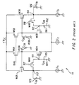
- FIG. 2 is a schematic diagram of a typical comparator which may be used as comparators 11, 12, and 13 of Figure 1. Reference numerals in Figure 2 are shown referred to comparator 11 of Figure 1. As shown in Figure 2, comparator 11 includes non-inverting input terminal 111 and inverting input terminal 112. Comparator 11 of Figure 2 is shown in the auto-zero mode. For AC analysis, input capacitors 115 and 116 are shown connected from input nodes 111 and 112, respectively to ground. Comparator 11 also includes inverting output terminal 113, and non-inverting output terminal 114. Output load capacitances 125 and 126 are shown connected between output terminals 113 and 114, respectively, and ground.
- Switch 117 is provided by transistor M4A, having current handling terminals connected between inverting output terminal 113 and non-inverting input terminal 111.
- switch 118 is provided by transistor M4B having its current handling terminals connected between non-inverting output terminal 114 and inverting input terminal 112.
- Transistors M2A and M2B provide a differential transistor pair having their sources connected in common to current source I2 and their drains connected to load devices M1A and M1B, respectively. Connected to the drain of transistor M2A is parasitic capacitance 413A, which is due to the drain junctions of transistors M1A and M2A, and the gate of transistor M3A.
- transistor M2B Connected to the drain of transistor M2B is parasitic capacitance 413B, which is due to the drain junctions of transistors M1B and M2B, and the gate of transistor M3B.
- Transistors M3A and M3B serve as source followers connecting the drains of differential transistors M2A and M2B to output terminals 113 and 114, respectively.
- Current sources I1 and I3 serve as pull down loads for transistors M3A and M3B, respectively.
- comparator 11 The dominant pole of comparator 11 is
- the non-dominant poles are P nd1 ⁇ - g M3A C 1A , P nd2 ⁇ - 1 C 2A R on ;
- comparator 11 is not very effective at operating at low supply voltages and at high temperature because R on of transistor M4A is increased with lower supply voltages and with increasing temperature (i. e. transistor M4A is not turned on as hard).
- U. S. Patent 4,513,212 describes a circuit for automatically clamping the P wells of a CMOS integrated circuit to the most negative potential of the integrated circuit as a whole.
- U. S. Patent 4,665,326 describes a voltage comparator including offset correction circuits including a digital to analog convertor error register for providing correction voltages to a set of capacitors contained within the error circuit.
- U. S. Patent No. 4,417,160 describes a comparator including offset compensation in which a potential offset means is included in the auto-zero feedback loop having an offset comparable to the input offset of the threshold detector, thereby allowing the offset correction voltage to track the input offset voltage over time and temperature.
- 4,587,443 describes an auto-zero sample and hold circuit including switches for, during the hold period, minimizing the effect of offset voltages by connecting the output of the comparator to its input and reversing the interstage connections between two cascaded differential amplifiers.
- Patentschrift DD. 233898A1 describes a comparator including a feedback loop between the output of the comparator and the input of the first amplifier. Offset is further reduced by the use of a dummy transistor.
- European Patent Application 001 555 4A1 describes a comparator circuit including switch means for shorting out the differential input leads prior to reading an input signal.
- U. S. Patent No. 3,585,510 pertains to a comparator circuit and more particularly the threshold setting circuit connected to the input leads of the comparator circuit.
- U. S. Patent No. 4,163,947 describes an auto-zeroing integrator in which, during an auto-zero mode, the current flowing into the input of the integrator is measured and a charge is stored which thereafter provides an equal but opposite current to the input of the integrator.
- U. S. Patent 4,542,305 pertains to an impedance buffer
- U. S. Patent 4,739,192 pertains to a digital to analog convertor bit switch. "MOS Transistor Electronic Stablization of Thresholds," IBM Technical Disclosure Bulletin, Vol. 10, #3, August 1967, pp.
- 336-337 describes a circuit for allowing a first transistor to provide a bias current to a second transistor, with the current flowing through the second transistor setting the level of the substrate voltage of the second transistor.
- This substrate voltage is maintained relatively constant over a wide number of devices, regardless of process variations and the like. This allows a large number of devices to be manufactured having similar threshold voltage levels, regardless of process variations.
- a novel auto-zero comparator in which the on resistance of MOS switches serving as transfer gates used in the auto-zero mode to connect the output lead to the input lead is minimized without the need to increase the ratio of the MOS switches.
- the on resistance of the transfer gates is reduced by reducing the threshold voltage of the transfer gates, which in turn is accomplished by making the bulk to source voltage of the transfer gates equal to zero. This is accomplished by utilizing a replica bias circuit which, during the auto-zero mode, replicates the voltage on the source of the transfer gates and applies this replica bias voltage to the bulk of the transfer gates.
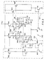
- FIG 3 is a schematic diagram of one embodiment of a comparator constructed in accordance with the teachings of this invention.
- Comparator 700 shown connected in the auto-zero mode, includes differential transistor pair M2A and M2B, and load devices M1A and M1B, as in the prior art circuit of Figure 2.
- Transistor M6 serves as a current source, analogous to current source I2 of the prior art circuit of Figure 2.
- Comparator 700 also includes common mode feedback circuit 701, as is known in the prior art, which operates to set the output voltage of comparator 700 by feedback controlling current source M6.
- the differential output voltage from output terminals 113 and 114 are applied to the gates of transistors M3A and M3B, respectively, thereby controlling the current flow through load device M5.
- the current flowing through load device M5 is mirrored by current source M6, thereby affecting the level of the output voltage on output terminals 113 and 114.
- This feedback loop assures a desired quiescent operating point for the differential output voltage, regardless of variations in temperature, power supply, voltage level, and the like.
- Transistor 711A and 711B are vertical NPN transistors and serve as a differential voltage clamp; thus limiting the differential output voltage swing to one diode drop. This helps to speed up the time for the circuit during the auto-zero mode of operation.
- switches 117 and 118 are formed as transistors M4A and M4B, respectively, serving as transmission gates connected between inverting output lead 113 and non-inverting input lead 111, and non-inverting output lead 114 and inverting lead 112, respectively.
- the substrates of transistors M4A and M4B are not connected to ground, but rather are connected to node 99 within a replica bias circuit 702 such that the voltage on the substrates of transistors M4A and M4B (which in one embodiment comprise one or more P wells in an N-type wafer) are set to equal the output voltages on output terminals 113 and 114.
- replica bias circuit 702 having transistor M1R connected to mirror the current flowing through transistor M1A, load device M2R serving to replicate transistor M2A, and current source M6R serving to replicate current source M6. Furthermore, transistors M3R and M5R serve to replicate transistors M3A and M3B of common mode feedback circuit 701.
- transistor M4A By applying a substrate voltage to transistor M4A which is equal to the voltage on inverting output lead 113, the on resistance R on of transistor M4A is minimized. It is well known that the resistance of an MOS transistor is defined:
- V T V TO + M[(V BS + 2 ⁇ ) 1 ⁇ 2 - (2 ⁇ ) 1 ⁇ 2 ] ;
- V BS equals zero and thus, from equation 11, V T approaches V TO .
- V T approaches V TO .
- R on becomes as low as possible.
- the ratio W/L of the channel width to channel length of transistor M4A need not be made large in an attempt to reduce R on , thereby obviating the need to undesirably increase the overlapped gate-to-source capacitance of transistor M4A and its associated increase in charge injection.
- the need for source follower M3A (Fig. 2) is obviated since the voltage swing on nodes 113 and 114 are more precisely controlled, e.g. by the limiting action of transistors 711A and 711B. This reduces integrated circuit die size, and in turn increases yield and reduces cost. In addition, without requiring source follower M3A, power consumption of the device is reduced.
- each unit of width and length being an arbitrary unit measurement for the purposes of showing relative sizes.
Landscapes
- Engineering & Computer Science (AREA)
- Power Engineering (AREA)
- Physics & Mathematics (AREA)
- Nonlinear Science (AREA)
- Theoretical Computer Science (AREA)
- Analogue/Digital Conversion (AREA)
- Manipulation Of Pulses (AREA)
- Measurement Of Current Or Voltage (AREA)
Claims (4)
- Eine Komparatorschaltung (700), umfassend:
eine erste Spannungsversorgungsklemme (Vcc);
eine zweite Spannungsversorgungsklemme;
eine erste Stromquelle (M6) mit einer Stromquellenklemme, die auf die zweite Spannungsversorgung bezogen ist;
einen invertierenden Eingangszweig, umfassend:
einen invertierenden Eingangstransistor (M2B) mit
einer invertierenden Eingangsleitung (112), einer ersten stromführenden Klemme, angeschlossen an die Stromquellenklemme, und einer zweiten stromführenden Klemme, die als nicht-invertierende Ausgangsklemme (114) dient; und
eine erste Lastkomponente (M1B), angeschlossen zwischen der ersten Spannungsversorgungsklemme und der zweiten stromführenden Klemme des invertierenden Eingangstransistors;
einen nichtinvertierenden Eingangszweig, umfassend:
einen nicht-invertierenden Eingangstransistor (M2A) mit einer
nicht-invertierenden Eingangsleitung (111), einer ersten stromführenden Klemme, angeschlossen an die Stromquellenklemme und einer zweiten stromführenden Klemme (113), die als eine invertierende Ausgangsklemme dient; und
eine zweite Lastkomponente (M1A), angeschlossen zwischen der ersten Spannungsversorgungsklemme und der zweiten stromführenden Klemme des nicht-invertierenden Eingangstransistors;
ein erstes Übertragungsgatter, umfassend einen ersten MOS-Transistor (M4b) mit einer ersten stromführenden Klemme, angeschlossen an die invertierende Eingangsleitung, einer zweiten stromführenden Klemme, angeschlossen an die nicht-invertierende Ausgangsleitung, einer Steuerklemme für den Empfang eines Steuersignals, das definiert, wann der erste MOS-Transistor durchzuschalten ist, und einer Massekleme, angeschlossen an die Masse des ersten MOS-Transistors;
ein zweites Übertragungsgatter, umfassend einen zweiten MOS-Transistor (M4A) mit einer ersten stromführenden Klemme, angeschlossen an die nicht-invertierende Eingangsleitung, einer zweiten stromführenden Klemme, angeschlossen an die invertierende Ausgangsleitung, einer Steuerklemme für den Empfang eines Steuersignals, das definiert, wann der zweite MOS-Transistor durchzuschalten ist, und einer Masseklemme, angeschlossen an die Masse des zweiten MOS-Transistors; und
Replika-Vorspannmittel (702) für das Bereitstellen einer Replika-Vorspannung für die erste und die zweite Masseklemme, welche Replika-Vorspannung im wesentlichen gleich ist der Spannung der invertierenden und der nicht-invertierenden Eingangsleitung, wenn das erste und das zweite Übertragungsgatter leitend sind. - Eine Schaltung nach Anspruch 1, bei der die Replika-Vorspannmittel umfassen:
eine dritte Lastkomponente (M1R), welche die erste und die zweite Lastkomponente dupliziert und mit einer ersten Leitung an die erste Spannungsversorgungsklemme angeschlossen ist sowie eine zweite Leitung aufweist,
eine zweite Stromklemme (M6R), welche die erste Stromquelle dupliziert und
eine vierte Lastkomponente (M2R), welche den invertierenden und den nicht-invertierenden Eingangstransistor dupliziert, angeschlossen zwischen der zweiten Leitung der dritten Lastkomponente und der zweiten Stromquelle. - Eine Schaltung nach Anspruch 1, die ferner einen Gleichtakt-Rückkopplungsschaltkreis (701) umfaßt, umfassend:
eine zweite Stromquelle (M5), derart angeschlossen, daß die erste Stromquelle den Strom, der von der zweiten Stromquelle bereitgestellt wird, widerspiegelt;
ein erstes Mittel (M3B), angeschlossen zwischen der invertierenden Ausgangsklemme (113) und der zweiten Stromquelle; und
ein zweites Mittel (M3A), angeschlossen zwischen der nicht-invertierenden Ausgangsklemme (114) und der zweiten Stromquelle;
bei welcher Schaltung ein gewünschter Ruhebetriebspunkt für die invertierenden und nicht-invertierenden Ausgangsspannungen aufrechterhalten wird. - Eine Schaltung nach Anspruch 3, bei der die Replika-Vorspannmittel umfassen:
eine dritte Lastkomponente, welche die erste und zweite Lastkomponente dupliziert, mit einer ersten Leitung angeschlossen an die erste Spannungsversorgungsklemme, und mit einer zweiten Leitung versehen;
eine dritte Stromquelle (M6R), welche die erste Stromquelle dupliziert;
eine vierte Stromquelle (M5R), welche die zweite Stromquelle dupliziert;
eine vierte Lastkomponente, welche den invertierenden und den nicht-invertierenden Eingangstransistor dupliziert, angeschlossen zwischen der zweiten Leitung der dritten Lastkomponente und der dritten Stromquelle; und
ein drittes Mittel (M3R), das das erste und das zweite Mittel des Gleichtakt-Rückkopplungsschaltkreises dupliziert.
Applications Claiming Priority (2)
| Application Number | Priority Date | Filing Date | Title |
|---|---|---|---|
| US07/379,577 US4962323A (en) | 1989-07-12 | 1989-07-12 | High speed auto zero comparator |
| US379577 | 1989-07-12 |
Publications (2)
| Publication Number | Publication Date |
|---|---|
| EP0407859A1 EP0407859A1 (de) | 1991-01-16 |
| EP0407859B1 true EP0407859B1 (de) | 1994-09-14 |
Family
ID=23497804
Family Applications (1)
| Application Number | Title | Priority Date | Filing Date |
|---|---|---|---|
| EP90112656A Expired - Lifetime EP0407859B1 (de) | 1989-07-12 | 1990-07-03 | Hochgeschwindigkeitskomparator mit automatischer Nullpunktseinstellung |
Country Status (5)
| Country | Link |
|---|---|
| US (1) | US4962323A (de) |
| EP (1) | EP0407859B1 (de) |
| JP (1) | JP3037972B2 (de) |
| KR (1) | KR0169966B1 (de) |
| DE (1) | DE69012464T2 (de) |
Cited By (2)
| Publication number | Priority date | Publication date | Assignee | Title |
|---|---|---|---|---|
| US6215333B1 (en) | 1997-03-27 | 2001-04-10 | Siemens Aktiengesellschaft | Comparator for a wide supply voltage range |
| US7649394B2 (en) | 2006-02-17 | 2010-01-19 | Zoran Corporation | Latch circuit |
Families Citing this family (20)
| Publication number | Priority date | Publication date | Assignee | Title |
|---|---|---|---|---|
| JP2760543B2 (ja) * | 1989-02-10 | 1998-06-04 | 株式会社東芝 | 多重帰還回路 |
| IT1236692B (it) * | 1989-11-10 | 1993-03-26 | St Microelectronics Srl | Dispositivo elettronico comparatore con isteresi. |
| US5182560A (en) * | 1989-12-22 | 1993-01-26 | Texas Instruments Incorporated | Analog-to-digital converter for high speed low power applications |
| US5084639A (en) * | 1990-09-17 | 1992-01-28 | General Electric Company | Low frequency noise canceling photodetector preamplifier useful for computerized tomography |
| US5065045A (en) * | 1990-10-04 | 1991-11-12 | Atmel Corporation | Multistage offset-cancelled voltage comparator |
| US5239210A (en) * | 1991-01-15 | 1993-08-24 | Crystal Semiconductor, Inc. | Low distortion unity gain amplifier for dac |
| IT1252392B (it) * | 1991-11-13 | 1995-06-12 | Sgs Thomson Microelectronics | Stadio transconduttore perfezionato per filtri ad alta frequenza |
| US5339067A (en) * | 1993-05-07 | 1994-08-16 | Crystal Semiconductor Corporation | Integrated voltage divider and circuit employing an integrated voltage divider |
| US5764175A (en) * | 1996-09-24 | 1998-06-09 | Linear Technology Corporation | Dual resolution circuitry for an analog-to-digital converter |
| US6429697B1 (en) * | 1999-10-05 | 2002-08-06 | Analog Devices, Inc. | Multi-stage, low-offset, fast-recovery, comparator system and method |
| TW455489B (en) | 1999-10-12 | 2001-09-21 | Takano Co Ltd | Rolling walker |
| US6340903B1 (en) | 2000-05-10 | 2002-01-22 | Zilog, Ind. | Auto-zero feedback sample-hold system |
| US6975150B2 (en) * | 2003-06-27 | 2005-12-13 | Intel Corporation | Apparatus and methods to control laser duty cycle |
| EP2057735B1 (de) * | 2006-08-28 | 2012-07-25 | ST-Ericsson SA | Schaltung zur umwandlung von differenz zu asymmetrisch und die schaltung verwendender komparator |
| US7567197B2 (en) * | 2007-09-17 | 2009-07-28 | Samsung Electronics Co., Ltd. | Cascade comparator and control method thereof |
| EP2124333B1 (de) | 2008-05-23 | 2013-01-02 | Zoran Corporation | Komparatorschaltung |
| US9503059B1 (en) | 2015-09-30 | 2016-11-22 | Integrated Device Technology, Inc. | Integrated circuit devices having oscillator circuits therein that support fixed frequency generation over process-voltage-temperature (PVT) variations |
| US10454488B1 (en) * | 2018-05-31 | 2019-10-22 | Analog Devices Global Unlimited Company | Variable speed comparator |
| US10972086B2 (en) | 2019-04-08 | 2021-04-06 | Texas Instruments Incorporated | Comparator low power response |
| EP4462676A1 (de) | 2023-05-12 | 2024-11-13 | Nxp B.V. | Verstärkerschaltung |
Family Cites Families (17)
| Publication number | Priority date | Publication date | Assignee | Title |
|---|---|---|---|---|
| US3655996A (en) * | 1969-03-13 | 1972-04-11 | Iwatsu Electric Co Ltd | Protective circuit for input circuit of junction type field effect transistor |
| US3585510A (en) * | 1969-06-02 | 1971-06-15 | Ibm | Threshold circuit apparatus having stabilized input level |
| DE2338981A1 (de) * | 1973-08-01 | 1975-02-13 | Laminex | Vorgeformte identifizierungskarte |
| US4163947A (en) * | 1977-09-23 | 1979-08-07 | Analogic Corporation | Current and voltage autozeroing integrator |
| JPS55118221A (en) * | 1979-03-06 | 1980-09-11 | Nec Corp | Comparison circuit |
| US4443717A (en) * | 1980-01-14 | 1984-04-17 | American Microsystems, Inc. | High resolution fast diode clamped comparator |
| US4417160A (en) * | 1981-07-30 | 1983-11-22 | Rca Corporation | Offset compensation apparatus for biasing an analog comparator |
| US4472648A (en) * | 1981-08-25 | 1984-09-18 | Harris Corporation | Transistor circuit for reducing gate leakage current in a JFET |
| US4665326A (en) * | 1981-11-03 | 1987-05-12 | Texas Instruments, Inc. | Voltage comparator |
| US4513212A (en) * | 1982-07-22 | 1985-04-23 | Electronics Pty. Ltd. | Automatic P-well clamping for CMOS integrated circuit |
| US4542305A (en) * | 1983-02-22 | 1985-09-17 | Signetics Corporation | Impedance buffer with reduced settling time |
| HU190567B (en) * | 1984-05-10 | 1986-09-29 | Budapesti Mueszaki Egyetem,Hu | Circuit arrangement for generating alternating current, for transferring thereof between circuits with different voltage and for stabilizing thereof |
| US4587443A (en) * | 1984-08-27 | 1986-05-06 | Signetics Corporation | Auto-zero sample and hold circuit |
| US4725813A (en) * | 1985-04-22 | 1988-02-16 | Nec Corporation | MOS type circuit device |
| US4739192A (en) * | 1987-02-24 | 1988-04-19 | Motorola, Inc. | Fast settling digital to analog converter bit switch |
| US4775807A (en) * | 1987-06-29 | 1988-10-04 | International Business Machines Corp. | Single ended receiver circuit with hysteresis |
| US4814648A (en) * | 1987-09-24 | 1989-03-21 | Texas Instruments Incorporated | Low 1/f noise amplifier for CCD imagers |
-
1989
- 1989-07-12 US US07/379,577 patent/US4962323A/en not_active Expired - Lifetime
-
1990
- 1990-07-03 EP EP90112656A patent/EP0407859B1/de not_active Expired - Lifetime
- 1990-07-03 DE DE69012464T patent/DE69012464T2/de not_active Expired - Fee Related
- 1990-07-11 KR KR1019900010476A patent/KR0169966B1/ko not_active Expired - Fee Related
- 1990-07-12 JP JP2182851A patent/JP3037972B2/ja not_active Expired - Fee Related
Cited By (2)
| Publication number | Priority date | Publication date | Assignee | Title |
|---|---|---|---|---|
| US6215333B1 (en) | 1997-03-27 | 2001-04-10 | Siemens Aktiengesellschaft | Comparator for a wide supply voltage range |
| US7649394B2 (en) | 2006-02-17 | 2010-01-19 | Zoran Corporation | Latch circuit |
Also Published As
| Publication number | Publication date |
|---|---|
| EP0407859A1 (de) | 1991-01-16 |
| KR910003944A (ko) | 1991-02-28 |
| DE69012464D1 (de) | 1994-10-20 |
| KR0169966B1 (ko) | 1999-03-30 |
| JPH0396119A (ja) | 1991-04-22 |
| JP3037972B2 (ja) | 2000-05-08 |
| US4962323A (en) | 1990-10-09 |
| DE69012464T2 (de) | 1995-05-04 |
Similar Documents
| Publication | Publication Date | Title |
|---|---|---|
| US4962323A (en) | High speed auto zero comparator | |
| US5541538A (en) | High speed comparator | |
| US5838200A (en) | Differential amplifier with switched capacitor common mode feedback | |
| US5359294A (en) | Charge-balanced switched-capacitor circuit and amplifier circuit using same | |
| KR0142565B1 (ko) | 전압 비교기 및 그 동작 방법 | |
| KR0175299B1 (ko) | Fet 비교기 회로 | |
| EP0101571A1 (de) | Spannungsdifferenz-Verstärker | |
| US4523107A (en) | Switched capacitor comparator | |
| EP0849883A1 (de) | Analog-Digital-Wandler | |
| US4573020A (en) | Fully differential operational amplifier with D.C. common-mode feedback | |
| US8410820B2 (en) | High speed latch comparators | |
| KR930000820B1 (ko) | 샘플 및 홀드회로 | |
| KR890004654B1 (ko) | 비교기회로 | |
| US6628148B2 (en) | Sample and hold circuit having a single control signal | |
| CN115118237A (zh) | 全差分运算放大器和全差分运算放大器电路 | |
| Liu et al. | Realisation of analogue divider using current feedback amplifiers | |
| US5625304A (en) | Voltage comparator requiring no compensating offset voltage | |
| US4577162A (en) | Clocked gain stage having differential inputs and outputs | |
| JPH08330857A (ja) | 演算増幅器 | |
| EP0349205B1 (de) | Differential-Analogkomparator | |
| GB2157108A (en) | Eliminating input offset | |
| KR0149307B1 (ko) | 정착시간이 빠른 연산증폭기 | |
| CN121417834A (zh) | 运算放大器及芯片 | |
| JP3063349B2 (ja) | 電圧比較装置 | |
| JPH02128523A (ja) | オフセット補正回路 |
Legal Events
| Date | Code | Title | Description |
|---|---|---|---|
| PUAI | Public reference made under article 153(3) epc to a published international application that has entered the european phase |
Free format text: ORIGINAL CODE: 0009012 |
|
| AK | Designated contracting states |
Kind code of ref document: A1 Designated state(s): DE FR GB IT NL |
|
| RIN1 | Information on inventor provided before grant (corrected) |
Inventor name: TA, PAUL DUC |
|
| 17P | Request for examination filed |
Effective date: 19910521 |
|
| 17Q | First examination report despatched |
Effective date: 19930804 |
|
| GRAA | (expected) grant |
Free format text: ORIGINAL CODE: 0009210 |
|
| AK | Designated contracting states |
Kind code of ref document: B1 Designated state(s): DE FR GB IT NL |
|
| REF | Corresponds to: |
Ref document number: 69012464 Country of ref document: DE Date of ref document: 19941020 |
|
| ET | Fr: translation filed | ||
| ITF | It: translation for a ep patent filed | ||
| PG25 | Lapsed in a contracting state [announced via postgrant information from national office to epo] |
Ref country code: GB Effective date: 19950703 |
|
| PLBE | No opposition filed within time limit |
Free format text: ORIGINAL CODE: 0009261 |
|
| STAA | Information on the status of an ep patent application or granted ep patent |
Free format text: STATUS: NO OPPOSITION FILED WITHIN TIME LIMIT |
|
| 26N | No opposition filed | ||
| PG25 | Lapsed in a contracting state [announced via postgrant information from national office to epo] |
Ref country code: NL Effective date: 19960201 |
|
| GBPC | Gb: european patent ceased through non-payment of renewal fee |
Effective date: 19950703 |
|
| NLV4 | Nl: lapsed or anulled due to non-payment of the annual fee |
Effective date: 19960201 |
|
| PG25 | Lapsed in a contracting state [announced via postgrant information from national office to epo] |
Ref country code: FR Effective date: 19960430 |
|
| REG | Reference to a national code |
Ref country code: FR Ref legal event code: ST |
|
| REG | Reference to a national code |
Ref country code: FR Ref legal event code: ST |
|
| REG | Reference to a national code |
Ref country code: FR Ref legal event code: ST |
|
| PG25 | Lapsed in a contracting state [announced via postgrant information from national office to epo] |
Ref country code: IT Free format text: LAPSE BECAUSE OF NON-PAYMENT OF DUE FEES;WARNING: LAPSES OF ITALIAN PATENTS WITH EFFECTIVE DATE BEFORE 2007 MAY HAVE OCCURRED AT ANY TIME BEFORE 2007. THE CORRECT EFFECTIVE DATE MAY BE DIFFERENT FROM THE ONE RECORDED. Effective date: 20050703 |
|
| PGFP | Annual fee paid to national office [announced via postgrant information from national office to epo] |
Ref country code: DE Payment date: 20070831 Year of fee payment: 18 |
|
| PG25 | Lapsed in a contracting state [announced via postgrant information from national office to epo] |
Ref country code: DE Free format text: LAPSE BECAUSE OF NON-PAYMENT OF DUE FEES Effective date: 20090203 |