EP0407250A1 - Detektor von elektromagnetischen Wellen - Google Patents
Detektor von elektromagnetischen Wellen Download PDFInfo
- Publication number
- EP0407250A1 EP0407250A1 EP90401714A EP90401714A EP0407250A1 EP 0407250 A1 EP0407250 A1 EP 0407250A1 EP 90401714 A EP90401714 A EP 90401714A EP 90401714 A EP90401714 A EP 90401714A EP 0407250 A1 EP0407250 A1 EP 0407250A1
- Authority
- EP
- European Patent Office
- Prior art keywords
- layers
- energy
- level
- detector according
- materials
- Prior art date
- Legal status (The legal status is an assumption and is not a legal conclusion. Google has not performed a legal analysis and makes no representation as to the accuracy of the status listed.)
- Granted
Links
- 239000000463 material Substances 0.000 claims description 39
- 238000005381 potential energy Methods 0.000 claims description 23
- 239000004065 semiconductor Substances 0.000 claims description 15
- 230000005684 electric field Effects 0.000 claims description 13
- 238000001514 detection method Methods 0.000 claims description 9
- 229910001218 Gallium arsenide Inorganic materials 0.000 claims description 7
- 238000010521 absorption reaction Methods 0.000 claims description 5
- 238000004519 manufacturing process Methods 0.000 claims description 3
- 230000005855 radiation Effects 0.000 claims description 2
- 239000000758 substrate Substances 0.000 claims description 2
- 230000004888 barrier function Effects 0.000 abstract description 26
- 230000007704 transition Effects 0.000 description 15
- 230000004044 response Effects 0.000 description 9
- 230000000694 effects Effects 0.000 description 8
- 238000010586 diagram Methods 0.000 description 7
- 238000005286 illumination Methods 0.000 description 7
- JBRZTFJDHDCESZ-UHFFFAOYSA-N AsGa Chemical compound [As]#[Ga] JBRZTFJDHDCESZ-UHFFFAOYSA-N 0.000 description 6
- 230000005274 electronic transitions Effects 0.000 description 6
- 230000008878 coupling Effects 0.000 description 5
- 238000010168 coupling process Methods 0.000 description 5
- 238000005859 coupling reaction Methods 0.000 description 5
- 238000005036 potential barrier Methods 0.000 description 5
- 230000007423 decrease Effects 0.000 description 3
- 229910000980 Aluminium gallium arsenide Inorganic materials 0.000 description 2
- GYHNNYVSQQEPJS-UHFFFAOYSA-N Gallium Chemical compound [Ga] GYHNNYVSQQEPJS-UHFFFAOYSA-N 0.000 description 2
- 229910000661 Mercury cadmium telluride Inorganic materials 0.000 description 2
- 229910045601 alloy Inorganic materials 0.000 description 2
- 239000000956 alloy Substances 0.000 description 2
- MDPILPRLPQYEEN-UHFFFAOYSA-N aluminium arsenide Chemical compound [As]#[Al] MDPILPRLPQYEEN-UHFFFAOYSA-N 0.000 description 2
- 230000005672 electromagnetic field Effects 0.000 description 2
- 229910052733 gallium Inorganic materials 0.000 description 2
- 230000000737 periodic effect Effects 0.000 description 2
- 230000005641 tunneling Effects 0.000 description 2
- 230000005428 wave function Effects 0.000 description 2
- 229910052785 arsenic Inorganic materials 0.000 description 1
- RQNWIZPPADIBDY-UHFFFAOYSA-N arsenic atom Chemical compound [As] RQNWIZPPADIBDY-UHFFFAOYSA-N 0.000 description 1
- 230000008901 benefit Effects 0.000 description 1
- 239000000969 carrier Substances 0.000 description 1
- 238000000605 extraction Methods 0.000 description 1
- 230000004907 flux Effects 0.000 description 1
- 229910052732 germanium Inorganic materials 0.000 description 1
- GNPVGFCGXDBREM-UHFFFAOYSA-N germanium atom Chemical compound [Ge] GNPVGFCGXDBREM-UHFFFAOYSA-N 0.000 description 1
- 239000012535 impurity Substances 0.000 description 1
- 239000011810 insulating material Substances 0.000 description 1
- 230000004807 localization Effects 0.000 description 1
- QSHDDOUJBYECFT-UHFFFAOYSA-N mercury Chemical compound [Hg] QSHDDOUJBYECFT-UHFFFAOYSA-N 0.000 description 1
- 229910052753 mercury Inorganic materials 0.000 description 1
- 238000000034 method Methods 0.000 description 1
- 230000001737 promoting effect Effects 0.000 description 1
- 238000005086 pumping Methods 0.000 description 1
- 230000000717 retained effect Effects 0.000 description 1
- 229910052710 silicon Inorganic materials 0.000 description 1
- 239000010703 silicon Substances 0.000 description 1
- 230000003595 spectral effect Effects 0.000 description 1
Images


Classifications
-
- H—ELECTRICITY
- H01—ELECTRIC ELEMENTS
- H01L—SEMICONDUCTOR DEVICES NOT COVERED BY CLASS H10
- H01L29/00—Semiconductor devices adapted for rectifying, amplifying, oscillating or switching, or capacitors or resistors with at least one potential-jump barrier or surface barrier, e.g. PN junction depletion layer or carrier concentration layer; Details of semiconductor bodies or of electrodes thereof ; Multistep manufacturing processes therefor
- H01L29/02—Semiconductor bodies ; Multistep manufacturing processes therefor
- H01L29/12—Semiconductor bodies ; Multistep manufacturing processes therefor characterised by the materials of which they are formed
- H01L29/20—Semiconductor bodies ; Multistep manufacturing processes therefor characterised by the materials of which they are formed including, apart from doping materials or other impurities, only AIIIBV compounds
- H01L29/201—Semiconductor bodies ; Multistep manufacturing processes therefor characterised by the materials of which they are formed including, apart from doping materials or other impurities, only AIIIBV compounds including two or more compounds, e.g. alloys
- H01L29/205—Semiconductor bodies ; Multistep manufacturing processes therefor characterised by the materials of which they are formed including, apart from doping materials or other impurities, only AIIIBV compounds including two or more compounds, e.g. alloys in different semiconductor regions, e.g. heterojunctions
-
- B—PERFORMING OPERATIONS; TRANSPORTING
- B82—NANOTECHNOLOGY
- B82Y—SPECIFIC USES OR APPLICATIONS OF NANOSTRUCTURES; MEASUREMENT OR ANALYSIS OF NANOSTRUCTURES; MANUFACTURE OR TREATMENT OF NANOSTRUCTURES
- B82Y20/00—Nanooptics, e.g. quantum optics or photonic crystals
-
- H—ELECTRICITY
- H01—ELECTRIC ELEMENTS
- H01L—SEMICONDUCTOR DEVICES NOT COVERED BY CLASS H10
- H01L31/00—Semiconductor devices sensitive to infrared radiation, light, electromagnetic radiation of shorter wavelength or corpuscular radiation and specially adapted either for the conversion of the energy of such radiation into electrical energy or for the control of electrical energy by such radiation; Processes or apparatus specially adapted for the manufacture or treatment thereof or of parts thereof; Details thereof
- H01L31/0248—Semiconductor devices sensitive to infrared radiation, light, electromagnetic radiation of shorter wavelength or corpuscular radiation and specially adapted either for the conversion of the energy of such radiation into electrical energy or for the control of electrical energy by such radiation; Processes or apparatus specially adapted for the manufacture or treatment thereof or of parts thereof; Details thereof characterised by their semiconductor bodies
- H01L31/0352—Semiconductor devices sensitive to infrared radiation, light, electromagnetic radiation of shorter wavelength or corpuscular radiation and specially adapted either for the conversion of the energy of such radiation into electrical energy or for the control of electrical energy by such radiation; Processes or apparatus specially adapted for the manufacture or treatment thereof or of parts thereof; Details thereof characterised by their semiconductor bodies characterised by their shape or by the shapes, relative sizes or disposition of the semiconductor regions
- H01L31/035236—Superlattices; Multiple quantum well structures
Definitions
- the invention relates to an electromagnetic wave detector and more specifically a quantum well semiconductor wave detector.
- the first solution (a) consists in using semiconductor materials whose forbidden bandwidth is lower than the photonic energy h ⁇ of the wave to be detected which therefore makes it possible to pass electrons from the valence band to that conduction. These electrons are then collected using an external circuit and are the source of a photocurrent which allows detection (see Figure 1a).
- materials whose prohibited bandwidth is compatible with this type of operation in the medium infrared there may be mentioned II-VI alloys of the HgCdTe type and group IV-VI alloys of the PbSnTe type.
- the second solution (b) providing for the use of semiconductors having a forbidden bandwidth greater than the photonic energy to be detected, is possible by resorting to doping of the materials used.
- This doping makes it possible to reveal an electron donor level corresponding to the impurities at the origin of the doping. From this energy level, closer to the bottom of the conductlon band than the top of the valence band, being able to produce electronic transitions towards the conduction band, making free and detectable the electrons having undergone these transitions under the effect, in particular, of an infrared electromagnetic field (see FIG. 1b).
- doping silicon with arsenic (Si: As) or germanium with mercury (Ge: Hg) allows detection in a spectral range located, in wavelength, around 10 microns.
- the third solution (c) is based on the occurrence of electronic transitions between permitted energy levels (e1 and e2) within the conduction band of semiconductor quantum structures.
- FIG. 1c gives an example of this type of transition in a well having two discrete levels of energy allowed for the electrons.
- the application of an electric field to this type of configuration makes it possible, as indicated in FIGS. 2a and 2b, to extract preferentially from the well, the electrons located on the excited quantum level (e2 in FIG. 2a and e ′ 2 in Figure 2b).
- the collection in the external electrical circuit of these electrons coming from the second quantum level on which they were carried by an infrared illumination (h ⁇ ) allows the detection of this illumination.
- the solution object of the invention relates to this third type (c) of infrared detectors.
- the type of detector to which the invention applies is therefore based on the occurrence, under the effect of infrared illumination, of electronic transitions within the conductive band of semiconductor quantum wells.
- the operating principle of these detectors is therefore to use these transitions to place the electrons initially located on the fundamental level of the well, at an energy level allowing them to easily exit the well under the effect of an applied electric field. So far two configurations corresponding to the solutions of Figures 2a and 2b above have been proposed to make this type of operation possible.
- the solution in Figure 2a is to use a well quantum having two levels e1 and e2 of energy allowed for the electrons in the band of conductlon. Under the effect of an illumination represented by its photonic energy h ⁇ in FIG.
- FIG. 2b The configuration of FIG. 2b is based on the use of a well having only one linked level e1, separated from the top of the barrier forming the well by an energy close to the photonic energy h ⁇ of the electromagnetic wave. to be detected (see Figure 2b). The transitions occur between this level and a virtual level located on the continuum.
- FIGS. 3a and 3b respectively correspond to the two types of transitions which have just been mentioned in relation to Figures 2a and 2b.
- This type of structure is based on the periodic stacking of layers of a first material M1 and a second material M2. The prohibited bandwidths of the two materials are different in order to obtain potential wells for the electrons in the conduction band.
- the contact layers located on either side of the periodic region designated by MPQ can for example consist of layers of material M1 highly doped n and denoted M1 / n +. To increase the number of possible transitions, use is generally made of n-type doping of the MPQ area.
- the electrons located on the level e2 have a lower potential barrier O to cross than the electrons located on the level e1 retained under field in the well by a barrier ⁇ + h ⁇ ).
- the width of this barrier is thinner (12) for the e2 level than for the e1 level (11) and this because of the potential profile imprinted on the structure by the electric field used for the collection of photoelectrons.
- this potential barrier to be crossed limits the performance of the detector because it limits the difference in mobility in the transport perpendicular to the semiconductor layers between the electrons located on the e1 level and those located on the e2 level, the two levels being separated by l energy h ⁇ given by the central wavelength of the detector response curve.
- an electromagnetic wave detector for the wave detection (h ⁇ ) to be detected comprising: - a semiconductor structure having at least one stack of a first, second, third, fourth and fifth layer (1, 2, 3, 4 and 5) whose widths of the forbidden bands make it possible to obtain the following profile of potential energy corresponding to the bottom of the conduction band for the electrons: - relatively low energy for the first layer providing a reference (0) of energies; - intermediate energy for the second and third layer; - higher value energy for the fourth and fifth layer; - the total allowable energy corresponding to a first fundamental level (e1) being less than the potential energy (V1) of the bottom of the conduction band of one and the other of the materials used to manufacture the second and third layers , the total permitted energy corresponding to a second level (e2) being between the potential energy (V1) at the bottom of the conduction band of one and the other of the materials of the second and third layers and the energy potential (V1 + V2) from the bottom of the conduction band of one and the
- the invention also relates to an electromagnetic wave detector for detecting the wave (h ⁇ ) to be detected, comprising: - a semiconductor structure having at least one stack of a first, second, third, fourth and fifth layer, the widths of the prohibited bands of which make it possible to obtain the following profile of potential energy corresponding to the top of the valence band for the holes : - relatively low energy for the first layer providing an energy reference; - intermediate energy for the second and third layers; - higher value energy for the fourth and fifth layers, the total allowable energy corresponding to a first fundamental level (e1) being less than the potential energy (V1) of the top of the valence band of one and the other of the materials used to make the second and third layers, the total allowable energy corresponding to a second level (e2) being between the potential energy (V1) of the top of the valence band of one and the other of the materials of the second and third layers and the potential energy (V1 + V2) of the top of the valence band and both of the materials of the fourth and fifth layers (4,
- the invention is an infrared detector based on the occurrence of electronic transitions between two quantum levels e1 and e2 allowed for the electrons within the potential well whose profile is shown in FIG. 4a.
- Such a profile of the conduction band is obtained using a structure shown in FIG. 4b comprising a layer 1 of a first material Ma framed between two layers 2 and 3 of a second material Mb the assembly being itself framed by two layers 4 and 5 of a third material Mc.
- Layer 1 has a band gap less than that of layers 2 and 3 and the band gap of layers 2 and 3 is itself less than that of layers 4 and 5.
- Layers 1 to 5 therefore constitute a quantum well as shown in FIG. 4a constituting intermediate barriers or staggered barriers (B1, B2).
- This difference between the levels e1 and e2 can also be modified by the width d3 of the highest barrier in the case where it is thin enough to allow coupling between the levels e2 of two consecutive wells.
- the values of these different parameters will therefore have to be determined so that the device effectively exhibits a significant absorption and detectivity for the h ⁇ desired photonic energy.
- the invention is also based on the fact that the level e1 is located at a potential energy lower than V1 and that the level e2 is located at a potential energy between V1 and V1 + V2. In practice, we will seek to obtain an important value for ⁇ 1 in order to limit the dark current. It should also be noted that the production of this structure requires at least three materials M a , M b , M c of different prohibited bandwidth.
- staggered barrier detectors using a greater number of materials are also envisaged within the scope of the invention.
- a greater number of materials can indeed make it possible to increase the number of steps per barrier or to make the asymmetrical wells endowing them with different barriers on the right and on the left.
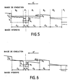
- the diagram of the conduction band becomes that of FIG. 5.
- the tunnel effect between the levels e1 of two consecutive wells is very strongly limited because of the barrier B1 + B2 + B′0, that is to say d2 + d3 + d2 to cross.
- the barrier height V1 + V2 greater in the central zone of width d3 than in the two contiguous zones of width d2, accentuates this limitation.
- the electrons located on the level e2 their perpendicular transport is facilitated by the low height of barrier ⁇ ′ 2 and the small thickness d3 of the barrier B2 (d3 ⁇ d3 + 2d2).
- the barrier ⁇ ⁇ 2 decreases faster than the barrier ⁇ ′1. Indeed, for a given field, the variation in potential with respect to the center of a well is greater at the distance d1 + d2 from this center than at the distance d1, which can be written: E ⁇ (d1 + d2)> E′d1.
- this original configuration makes it possible to favor the passage in the continuum, under the effect of an electric field, of the electrons located on the level e2, while maintaining an important barrier for the electrons located on the level e1 which n 'weren't excited by the wave at detect and whose transport perpendicular to the quantum layers corresponds to a dark current.
- the level e2 remains confined since its energy level is above V2. Consequently, since the electrons located on the levels e1 and e2 are confined in the region of the well, the probability of transition remains important contrary to what happens if one uses the known solution of figure 2b described previously.
- This original configuration therefore makes it possible to limit the dark current while increasing the response of detectors of the MPQ (Multi-Well Quantum) type.
- the width d3 of the barrier can also play an important role in this type of device. Indeed, if d3 is sufficiently large, taking into account the height of O 2 ′ , the wells can be considered as decoupled since the extensions of the wave functions will not allow this coupling between consecutive levels e2 and even less between levels e1 . If the dimension d3 is small enough to allow coupling between consecutive levels e2, a tunnel effect between these levels along the structure could take place under a weak applied field, which could favor the response of the detector in these low field conditions, therefore low dark current.
- FIG. 7 represents the conductlon strip of an exemplary embodiment of a structure according to the invention.
- This structure which is a detailed embodiment of the structure of FIG. 4b comprises: - a layer 1 of gallium arsenide; - layers 2 and 3 of gallium and aluminum arsenide of general formula Ga 1-x Al x As; by way of example in FIG. 7, x is 0.2 and the formula is Ga 0.8 A1 0.2 As; - layers 4 and 5 of gallium and aluminum arsenide of general formula Ga 1-y Al y As; by way of example in FIG. 7, y is worth 0.3 and the formula is Ga 0.7 A1 0.3 As.
- This structure constitutes a quantum well having a first level linked e1 lower than the potential energy (V1) of the bottom of the conduction band of the materials of layers 2 and 3, as well as two energy levels e2 and e3 such as the level e2 is between the bottom of the conduction band of the materials of layers 2 and 3 and the bottom of the conductive band of the materials of layers 4 and 5.
- V1 potential energy
- e2 and e3 energy levels
- the transitions useful for detection must occur between the levels e1 and e2.
- This structure has a certain number of energy levels 5 for example, that is to say the first level e1 and the second level e2 located as described above (at 89 meV and 206 meV) plus three levels e3, e4, e5.
- the useful transitions for detection must occur between the levels e1 and e2.
- Figure 9 shows a detector structure of the invention. We find layers 1 to 5 described above, reproduced several times as indicated by the dotted lines to form a quantum multi-well.
- the assembly is supported by a substrate 6 which may be made of semi-insulating material.
- Two electrodes E1 and E2 make it possible to apply an electric field to the structure under the control of a control generator MC.
- the electrode E1 has a window 7 making it possible to transmit a light flux h to be detected to the structure.
- the energy levels e1 of the quantum wells can be populated in electrons by doping as that indicated previously.
- These energy levels e1 can also be populated with electrons by illumination by a near-infrared pumping light wave supplied by means not shown.
- the detector operates and detects h ⁇ radiation when an electric field is applied by the MC generator.
- This detection is done using a DET current detector connected in series in the electric field application circuit.
- the invention therefore relates to the field of detecting an electromagnetic wave through the use of electronic transitions between discrete energy levels within the conduction band of quantum wells which can be associated in large numbers to increase the response. of this type of detectors.
- the existing solutions in this particular field do not make it possible to satisfactorily limit the dark current while retaining a sufficient response.
- the invention relates to a structure using for the two barriers which constitute the well, a stepped shape which makes it possible to operate the detector between two discrete levels e1 and e2 while promoting the extraction of the well, electrons located on the level e2 .
- This form of barrier amounts to giving the well a smaller dimension for the electrons located on the e1 level than for those located on the e2 level which nevertheless remain confined in the zone of the well, which allows to maintain a high probability of transition to e2.
- this original configuration makes it possible, when several of these wells are combined to increase the response of the device, to limit the dark current due in particular to the transport, from well to well, of electrons located on the level e1.
- the potential barrier "seen" by the electrons located on the level e2 is much weaker and facilitates the transport along the structure of these photo-excited electrons.
- the use of wells with stepped barriers makes it possible to optimize the response / dark current ratio.
- the levels e1 and e2 must be located: - for e1 at a level lower than the potential energy of the bottom of the conduction band of the materials of the two layers 2 and 3; - for e2 at a level between the potential energies of the bottom of the conduction bands of the materials of layers 2 and 3 on the other hand, and of layers 4 and 5 on the other hand.
Applications Claiming Priority (2)
| Application Number | Priority Date | Filing Date | Title |
|---|---|---|---|
| FR8908961 | 1989-07-04 | ||
| FR8908961A FR2649536B1 (fr) | 1989-07-04 | 1989-07-04 | Detecteur d'ondes electromagnetiques |
Publications (2)
| Publication Number | Publication Date |
|---|---|
| EP0407250A1 true EP0407250A1 (de) | 1991-01-09 |
| EP0407250B1 EP0407250B1 (de) | 1993-05-19 |
Family
ID=9383441
Family Applications (1)
| Application Number | Title | Priority Date | Filing Date |
|---|---|---|---|
| EP90401714A Expired - Lifetime EP0407250B1 (de) | 1989-07-04 | 1990-06-19 | Detektor von elektromagnetischen Wellen |
Country Status (4)
| Country | Link |
|---|---|
| US (1) | US5077466A (de) |
| EP (1) | EP0407250B1 (de) |
| DE (1) | DE69001648T2 (de) |
| FR (1) | FR2649536B1 (de) |
Cited By (2)
| Publication number | Priority date | Publication date | Assignee | Title |
|---|---|---|---|---|
| EP0463907A1 (de) * | 1990-06-26 | 1992-01-02 | Thomson-Csf | Detektor für elektromagnetischen Wellen |
| EP0578557A1 (de) * | 1992-07-07 | 1994-01-12 | Thomson-Csf | Quantum-Well-Detektor für elektromagnetische Wellen |
Families Citing this family (9)
| Publication number | Priority date | Publication date | Assignee | Title |
|---|---|---|---|---|
| FR2725081B1 (fr) * | 1994-09-23 | 1996-11-15 | Thomson Csf | Source optique compacte, basee sur le doublage de frequence d'un laser et auto-stabilisee par depeuplement de la pompe |
| US5539206A (en) * | 1995-04-20 | 1996-07-23 | Loral Vought Systems Corporation | Enhanced quantum well infrared photodetector |
| FR2749721B1 (fr) * | 1996-06-07 | 1998-11-27 | Thomson Csf | Commutateur electrique a photoconducteur |
| US5978399A (en) * | 1996-12-10 | 1999-11-02 | Doughty; Kathryn L. | Electrically-tunable infrared detectors and method based on intraband transitions in quantum well structures |
| DE19711505C1 (de) * | 1997-03-19 | 1998-08-27 | Fraunhofer Ges Forschung | Halbleiterheterostruktur-Strahlungsdetektor für Wellenlängen aus dem infraroten Spektralbereich |
| US6054718A (en) * | 1998-03-31 | 2000-04-25 | Lockheed Martin Corporation | Quantum well infrared photocathode having negative electron affinity surface |
| FR2784185B1 (fr) | 1998-10-06 | 2001-02-02 | Thomson Csf | Dispositif pour l'harmonisation entre une voie d'emission laser et une voie passive d'observation |
| FR2814281B1 (fr) * | 2000-09-19 | 2003-08-29 | Thomson Lcd | Matrice active tft pour capteur optique comportant une couche semi-conductrice photosensible, et capteur optique comportant une telle matrice |
| FR2825463B1 (fr) * | 2001-05-30 | 2003-09-12 | Thales Sa | Gyrometre laser etat solide comportant un bloc resonateur |
Citations (2)
| Publication number | Priority date | Publication date | Assignee | Title |
|---|---|---|---|---|
| US4671830A (en) * | 1984-01-03 | 1987-06-09 | Xerox Corporation | Method of controlling the modeling of the well energy band profile by interdiffusion |
| EP0299841A2 (de) * | 1987-07-17 | 1989-01-18 | Thomson-Csf | Detektor von elektromagnetischen Wellen und diesen Detektor anwendender Bildanalysator |
Family Cites Families (3)
| Publication number | Priority date | Publication date | Assignee | Title |
|---|---|---|---|---|
| FR2586804B1 (fr) * | 1985-08-30 | 1989-03-31 | Centre Nat Rech Scient | Procede et dispositif de photo-detection rapide a l'aide d'un superreseau |
| WO1988001792A1 (en) * | 1986-09-04 | 1988-03-10 | Varian Associates, Inc. | Superlattice for a semiconductor device |
| US4903101A (en) * | 1988-03-28 | 1990-02-20 | California Institute Of Technology | Tunable quantum well infrared detector |
-
1989
- 1989-07-04 FR FR8908961A patent/FR2649536B1/fr not_active Expired - Fee Related
-
1990
- 1990-06-19 EP EP90401714A patent/EP0407250B1/de not_active Expired - Lifetime
- 1990-06-19 DE DE9090401714T patent/DE69001648T2/de not_active Expired - Fee Related
- 1990-06-28 US US07/544,895 patent/US5077466A/en not_active Expired - Lifetime
Patent Citations (2)
| Publication number | Priority date | Publication date | Assignee | Title |
|---|---|---|---|---|
| US4671830A (en) * | 1984-01-03 | 1987-06-09 | Xerox Corporation | Method of controlling the modeling of the well energy band profile by interdiffusion |
| EP0299841A2 (de) * | 1987-07-17 | 1989-01-18 | Thomson-Csf | Detektor von elektromagnetischen Wellen und diesen Detektor anwendender Bildanalysator |
Non-Patent Citations (2)
| Title |
|---|
| APPLIED PHYSICS LETTERS, vol. 50, no. 16, 20 avril 1987, pages 1092-1094, New York, US; B.F. LEVINE et al.: "New 10 mum infrared detector using intersubband absorption in resonant tunneling GaAlAs superlattices" * |
| APPLIED PHYSICS LETTERS, vol. 53, no. 20, 14 novembre 1988, pages 1961-1963, New York, US; S.R. KURTZ et al.: "High photoconductive gain in InAsSb strained-layer superlattice infrared detectors" * |
Cited By (5)
| Publication number | Priority date | Publication date | Assignee | Title |
|---|---|---|---|---|
| EP0463907A1 (de) * | 1990-06-26 | 1992-01-02 | Thomson-Csf | Detektor für elektromagnetischen Wellen |
| US5355000A (en) * | 1990-06-26 | 1994-10-11 | Thomson-Csf | Assymetric quantum well infrared detector |
| EP0578557A1 (de) * | 1992-07-07 | 1994-01-12 | Thomson-Csf | Quantum-Well-Detektor für elektromagnetische Wellen |
| FR2693594A1 (fr) * | 1992-07-07 | 1994-01-14 | Thomson Csf | Détecteur d'ondes électromagnétiques à puits quantiques. |
| US5506418A (en) * | 1992-07-07 | 1996-04-09 | Thomson-Csf | Electromagnetic wave detector with quantum well structure |
Also Published As
| Publication number | Publication date |
|---|---|
| FR2649536A1 (fr) | 1991-01-11 |
| DE69001648D1 (de) | 1993-06-24 |
| FR2649536B1 (fr) | 1994-07-22 |
| EP0407250B1 (de) | 1993-05-19 |
| DE69001648T2 (de) | 1993-09-02 |
| US5077466A (en) | 1991-12-31 |
Similar Documents
| Publication | Publication Date | Title |
|---|---|---|
| EP1756872B1 (de) | Mesastruktur-photonerkennungschaltung | |
| EP2715808B1 (de) | Halbleiterstruktur zur ausstrahlung von licht und verfahren zur herstellung einer solchen struktur | |
| FR2663787A1 (fr) | Detecteur d'ondes electromagnetiques. | |
| EP3084843B1 (de) | Quantendetektionselement mit geringem rauschen und verfahren zur herstellung solch eines lichtdetektionselements | |
| EP0236189B1 (de) | Monolithische Halbleiterstruktur eines Bipoltransistors mit Heteroübergängen und eines Lasers | |
| FR2655434A1 (fr) | Dispositif optique a puits quantiques et procede de realisation. | |
| EP0407250B1 (de) | Detektor von elektromagnetischen Wellen | |
| EP0578557A1 (de) | Quantum-Well-Detektor für elektromagnetische Wellen | |
| EP0566494B1 (de) | Elektronenstrahl gepumpter Laserresonator mit asymmetrischer Halbleiter-Heterostruktur | |
| EP3012876A1 (de) | Herstellungsverfahren einer rauscharmen fotodiode | |
| FR2686456A1 (fr) | Detecteur infrarouge a puits quantiques. | |
| EP2937902B1 (de) | Matrix aus cdhgte-fotodioden | |
| EP2359414B1 (de) | Infrarotdetektor mit erweitertem spektralen ansprechverhalten im sichtbaren feld | |
| FR2758657A1 (fr) | Photodetecteur metal-semiconducteur-metal | |
| WO2014053386A1 (fr) | Dispositif electronique comprenant des nanostructures en filaments et procede de fabrication de tels dispositifs | |
| EP3353818A1 (de) | Fotodetektor mit einem stapel aus vertikal angrenzenden schichten | |
| EP0082787B1 (de) | Photodiode mit getrennten Absorptions- und Avalanchezonen | |
| WO2011012833A2 (fr) | Dispositifs electro-optiques bases sur la variation d'indice ou d'absorption dans des transitions isb | |
| FR2719417A1 (fr) | Composant à hétérostructure semi-conductrice, commande par la lumière pour la génération d'oscillations hyperfréquences. | |
| EP0511057B1 (de) | Wellenmodulator und optischer Detektor mit Quantenpotentialtöpfen | |
| EP0557186B1 (de) | Photoelektrischer Detektor mit Quantentöpfen und verbesserter Detectivität | |
| EP2592663B1 (de) | Lichtemittierende Vorrichtung mit entgegengesetzten p-Typ und n-Typ Transistoren, und Herstellungsverfahren | |
| FR2562715A1 (fr) | Photodetecteur a avalanche | |
| EP2141779A1 (de) | Vorrichtung vom Typ Quantenkaskadendetektor mit Hochinjektor | |
| FR2667165A1 (fr) | Modulateur electrooptique multicouche de lumiere. |
Legal Events
| Date | Code | Title | Description |
|---|---|---|---|
| PUAI | Public reference made under article 153(3) epc to a published international application that has entered the european phase |
Free format text: ORIGINAL CODE: 0009012 |
|
| AK | Designated contracting states |
Kind code of ref document: A1 Designated state(s): DE FR GB |
|
| 17P | Request for examination filed |
Effective date: 19910322 |
|
| 17Q | First examination report despatched |
Effective date: 19920210 |
|
| GRAA | (expected) grant |
Free format text: ORIGINAL CODE: 0009210 |
|
| AK | Designated contracting states |
Kind code of ref document: B1 Designated state(s): DE FR GB |
|
| REF | Corresponds to: |
Ref document number: 69001648 Country of ref document: DE Date of ref document: 19930624 |
|
| GBT | Gb: translation of ep patent filed (gb section 77(6)(a)/1977) |
Effective date: 19930713 |
|
| RAP2 | Party data changed (patent owner data changed or rights of a patent transferred) |
Owner name: THOMSON-CSF |
|
| PLBE | No opposition filed within time limit |
Free format text: ORIGINAL CODE: 0009261 |
|
| STAA | Information on the status of an ep patent application or granted ep patent |
Free format text: STATUS: NO OPPOSITION FILED WITHIN TIME LIMIT |
|
| 26N | No opposition filed | ||
| REG | Reference to a national code |
Ref country code: GB Ref legal event code: IF02 |
|
| REG | Reference to a national code |
Ref country code: FR Ref legal event code: CD |
|
| PGFP | Annual fee paid to national office [announced via postgrant information from national office to epo] |
Ref country code: DE Payment date: 20070614 Year of fee payment: 18 |
|
| PGFP | Annual fee paid to national office [announced via postgrant information from national office to epo] |
Ref country code: GB Payment date: 20070613 Year of fee payment: 18 |
|
| PGFP | Annual fee paid to national office [announced via postgrant information from national office to epo] |
Ref country code: FR Payment date: 20070608 Year of fee payment: 18 |
|
| GBPC | Gb: european patent ceased through non-payment of renewal fee |
Effective date: 20080619 |
|
| REG | Reference to a national code |
Ref country code: FR Ref legal event code: ST Effective date: 20090228 |
|
| PG25 | Lapsed in a contracting state [announced via postgrant information from national office to epo] |
Ref country code: DE Free format text: LAPSE BECAUSE OF NON-PAYMENT OF DUE FEES Effective date: 20090101 |
|
| PG25 | Lapsed in a contracting state [announced via postgrant information from national office to epo] |
Ref country code: GB Free format text: LAPSE BECAUSE OF NON-PAYMENT OF DUE FEES Effective date: 20080619 |
|
| PG25 | Lapsed in a contracting state [announced via postgrant information from national office to epo] |
Ref country code: FR Free format text: LAPSE BECAUSE OF NON-PAYMENT OF DUE FEES Effective date: 20080630 |