EP0405865B1 - Verfahren zum Verbinden gegenüberliegender Paare von Detektor- und Auslesemikrochipkontakten in einer Hybriddetektoranordnung - Google Patents
Verfahren zum Verbinden gegenüberliegender Paare von Detektor- und Auslesemikrochipkontakten in einer Hybriddetektoranordnung Download PDFInfo
- Publication number
- EP0405865B1 EP0405865B1 EP90306877A EP90306877A EP0405865B1 EP 0405865 B1 EP0405865 B1 EP 0405865B1 EP 90306877 A EP90306877 A EP 90306877A EP 90306877 A EP90306877 A EP 90306877A EP 0405865 B1 EP0405865 B1 EP 0405865B1
- Authority
- EP
- European Patent Office
- Prior art keywords
- indium
- columns
- tubes
- detector
- array
- Prior art date
- Legal status (The legal status is an assumption and is not a legal conclusion. Google has not performed a legal analysis and makes no representation as to the accuracy of the status listed.)
- Expired - Lifetime
Links
Images

Classifications
-
- H—ELECTRICITY
- H10—SEMICONDUCTOR DEVICES; ELECTRIC SOLID-STATE DEVICES NOT OTHERWISE PROVIDED FOR
- H10W—GENERIC PACKAGES, INTERCONNECTIONS, CONNECTORS OR OTHER CONSTRUCTIONAL DETAILS OF DEVICES COVERED BY CLASS H10
- H10W72/00—Interconnections or connectors in packages
- H10W72/20—Bump connectors, e.g. solder bumps or copper pillars; Dummy bumps; Thermal bumps
-
- H—ELECTRICITY
- H10—SEMICONDUCTOR DEVICES; ELECTRIC SOLID-STATE DEVICES NOT OTHERWISE PROVIDED FOR
- H10F—INORGANIC SEMICONDUCTOR DEVICES SENSITIVE TO INFRARED RADIATION, LIGHT, ELECTROMAGNETIC RADIATION OF SHORTER WAVELENGTH OR CORPUSCULAR RADIATION
- H10F39/00—Integrated devices, or assemblies of multiple devices, comprising at least one element covered by group H10F30/00, e.g. radiation detectors comprising photodiode arrays
- H10F39/10—Integrated devices
- H10F39/12—Image sensors
- H10F39/191—Photoconductor image sensors
- H10F39/193—Infrared image sensors
- H10F39/1935—Infrared image sensors of the hybrid type
-
- H—ELECTRICITY
- H10—SEMICONDUCTOR DEVICES; ELECTRIC SOLID-STATE DEVICES NOT OTHERWISE PROVIDED FOR
- H10W—GENERIC PACKAGES, INTERCONNECTIONS, CONNECTORS OR OTHER CONSTRUCTIONAL DETAILS OF DEVICES COVERED BY CLASS H10
- H10W90/00—Package configurations
-
- H—ELECTRICITY
- H05—ELECTRIC TECHNIQUES NOT OTHERWISE PROVIDED FOR
- H05K—PRINTED CIRCUITS; CASINGS OR CONSTRUCTIONAL DETAILS OF ELECTRIC APPARATUS; MANUFACTURE OF ASSEMBLAGES OF ELECTRICAL COMPONENTS
- H05K3/00—Apparatus or processes for manufacturing printed circuits
- H05K3/30—Assembling printed circuits with electric components, e.g. with resistors
- H05K3/32—Assembling printed circuits with electric components, e.g. with resistors electrically connecting electric components or wires to printed circuits
- H05K3/34—Assembling printed circuits with electric components, e.g. with resistors electrically connecting electric components or wires to printed circuits by soldering
- H05K3/3465—Application of solder
- H05K3/3478—Application of solder preforms; Transferring prefabricated solder patterns
-
- H—ELECTRICITY
- H10—SEMICONDUCTOR DEVICES; ELECTRIC SOLID-STATE DEVICES NOT OTHERWISE PROVIDED FOR
- H10W—GENERIC PACKAGES, INTERCONNECTIONS, CONNECTORS OR OTHER CONSTRUCTIONAL DETAILS OF DEVICES COVERED BY CLASS H10
- H10W72/00—Interconnections or connectors in packages
- H10W72/20—Bump connectors, e.g. solder bumps or copper pillars; Dummy bumps; Thermal bumps
- H10W72/231—Shapes
- H10W72/234—Cross-sectional shape, i.e. in side view
-
- H—ELECTRICITY
- H10—SEMICONDUCTOR DEVICES; ELECTRIC SOLID-STATE DEVICES NOT OTHERWISE PROVIDED FOR
- H10W—GENERIC PACKAGES, INTERCONNECTIONS, CONNECTORS OR OTHER CONSTRUCTIONAL DETAILS OF DEVICES COVERED BY CLASS H10
- H10W72/00—Interconnections or connectors in packages
- H10W72/20—Bump connectors, e.g. solder bumps or copper pillars; Dummy bumps; Thermal bumps
- H10W72/251—Materials
-
- Y—GENERAL TAGGING OF NEW TECHNOLOGICAL DEVELOPMENTS; GENERAL TAGGING OF CROSS-SECTIONAL TECHNOLOGIES SPANNING OVER SEVERAL SECTIONS OF THE IPC; TECHNICAL SUBJECTS COVERED BY FORMER USPC CROSS-REFERENCE ART COLLECTIONS [XRACs] AND DIGESTS
- Y10—TECHNICAL SUBJECTS COVERED BY FORMER USPC
- Y10T—TECHNICAL SUBJECTS COVERED BY FORMER US CLASSIFICATION
- Y10T29/00—Metal working
- Y10T29/49—Method of mechanical manufacture
- Y10T29/49002—Electrical device making
- Y10T29/49117—Conductor or circuit manufacturing
- Y10T29/49169—Assembling electrical component directly to terminal or elongated conductor
Definitions
- This invention relates to electrical connectors for infrared detectors and, more particularly, to arrangements for improving the reliability of connections to a plurality of sensors in a detector array assembly which is subject to thermal fatigue from temperature cycling.
- the hybrid detector array assembly comprises a pair of microchips, one bearing the array of sensors and the other bearing a corresponding array of cells or diodes with associated contact pads to provide the readout of individual sensor signals.
- the contact pairs of the two microchips are joined together in a process called hydridization.
- a plurality of indium bumps on the detector chip and a corresponding plurality of indium bumps on the readout chip are cold welded together by pressure. Once joined, they are no longer separable and the breaking of any weld constitutes a failure of that readout cell.
- an infrared detector array is repeatedly cycled between room temperature and its normal operating temperature of 77 degrees K. This repeated temperature cycling is responsible for problems relating to thermal fatigue which results from the different coefficients of thermal expansion in the different materials present in the hybrid detector assembly.
- the indium bumps are made by vapor deposition through a photo-reduced mask pattern and have a typical height of 6-9 »m. It is not possible to deposit the indium bumps more than 10 »m high with acceptable quality and density.
- the various materials present in the array account for the thermal fatigue problems.
- the readout chip is a silicon substrate with contact pads approximately 25.4 »m (0.001 inch) square on 50.8 »m (0.002 inch) spacing.
- a typical array may have 128x128 cells.
- the sensors are arranged in a similar array on a cadmium telluride substrate.
- the resulting more compliant arrangement is expected to exhibit more tolerance for the effects of thermal expansion and contraction during repeated temperature excursions between room temperature and operating temperature.
- the present invention provides a method of forming a hybrid detector array assembly comprising an array of connector columns extending between opposed pairs of contacts of respective detector and readout microchips which are to be interconnected, the method comprising the steps of: providing an interconnector pad having a plurality of hollow metal tubes mounted in a film carrier, which tubes are positioned in an array corresponding to respective arrays of contacts on the detector and readout microchips; dipping the ends of the tubes in a selected molten filler metal to induce the metal to fill the tubes by capillary action; cooling the interconnector pad to solidify the filler metal, thereby forming an array of filler metal columns located inside the said tubes; connecting a first end of the array of filler metal columns to the respective array of contacts on the detector chip or on the readout chip; followed by etching away the metal tubes and removing the film carrier; followed by connecting a second end of the array of filler metal columns to the respective array of contacts on the readout chip or the detector chip.
- a preferred type of interconnector pad for the practice of the present invention is marketed by Raychem Corporation, Menlo Park, California, under the trademark Uniax. It consists of a high performance polymer film as a carrier for an array of metal tubes which extend through the film and protrude from each side. Typical dimensions of the Uniax Integrated circuit connector are: a film thickness of 75 »m, tube diameter of 40 »m, tube spacing of 80 »m, wall thickness of 10 »m and protrusion from the polymer film on each side of 20 »m.
- Such an interconnect pad can be fabricated by forming a sandwich or laminate of three layers of two different, differentially etchable materials.
- a laser is used to drill holes through the laminate using a mask pattern corresponding to the detector array, followed by through-hole plating with copper, nickel, or some other suitable material to form a plurality of miniature tubes.
- the top and bottom layers of the laminate are then removed by etching, leaving the middle polymer layer as a carrier film of the metal tubes.
- the articles comprise electrically insulating sheet material having a pattern of through-holes corresponding to the said patterns of connection sites, each of which holes is not more than 200 micrometres in diameter and is internally plated with electrically conductive material which provides an electrically conductive path between, and projects beyond but not significantly along, the main surfaces of the sheet material to make electrical connections between facing pairs of the connection sites when the sheet material in use is arranged between the substrates with the conductive material in each of the said through-holes aligned between and in contact with its corresponding pair of connection sites.
- the through-holes are filled with a flowable electrically conductive material, such as indium, which is used to form the connections between the substrates.
- the uniaxial article is then removed, to leave pillars of the flowable electrically conductive material forming the connections between the substrates.
- the hybrid detector array assembly is a focal plane array assembly
- the method further comprises the steps of: using the focal plane array pattern to make a photo-reduced mask; using an interconnect pad with copper tubes which corresponds to the focal plane array mask and specification therefor; cleaning and preparing the interconnect pad for a dipping process; dipping the pad in molten indium and continuing the dip until the tubes are filled with indium by capillary action; transferring the indium-filled tubes to the readout chip and affixing them at one end to the individual contact pads on the readout chip by cold welding to indium bumps on the pads; etching out the original copper tubes with ammonium sulphate to release the carrier film; lifting off the carrier film from the array of indium columns; and placing the detector chip in aligned position with the indium columns and cold welding the upper ends of the columns to indium bumps on the sensor contacts by pressure welding.
- the ultra-tall indium or alloy columns fashioned in accordance with the invention and connected between the sensor contacts and the readout contact pads provide a compliant structural coupling between the detector and readout chips which enables the combination, i.e., the hybrid detector assembly to accommodate the effects of differential thermal expansion so that the deleterious results of thermal fatigue as described above--breaking off pieces of contacts, pulling contact pads away from the substrate, warpage, etc.--are avoided.
- molten solder alloy in place of the molten indium as a filler for the interconnecting tubes, a molten solder alloy may be used. This alloy will be a material which is suitable for attachment to the indium bumps by the hybridization process.
- nickel capillary tubes may be used in place of the copper tubes. A suitable etchant for nickel would have to be used in the tube etching step.
- the standard interconnect pads provide the necessary temporary interconnections between the detector and readout chips for the test evaluation. If the detector chip is found to be free of defects and suitable for use, the processing of the interconnect pads to form the ultra-tall indium columns and to attach the columns to the contact arrays of the respective detector and readout chips is completed, as described hereinabove.
- different forms of extended indium columns may be developed to serve different purposes.
- separate indium columns may be attached respectively to the pads on the silicon substrate of the readout chip and to the contact mesas of the detector chip.
- the separate indium columns can then be connected at their adjacent ends to form a series of taller indium columns providing additional spacing between the detector and readout chips with correspondingly increased compliance to accommodate the thermal expansion and contraction.
- the individual connector tubes are generally tapered because of the way in which they are formed by a laser beam. If the smaller ends of the tubes are joined together in accordance with this aspect of the invention, the result is a configuration having a shape somewhat like that of an hourglass which exhibits improved flexibility and compliance under thermal expansion and contraction.
- multi-layer plating is used to develop a higher aspect ratio for the indium columns.
- This process begins with electroless plated copper tubes which, prior to being filled with indium, are given a layer of electroless nickel plated on the inside of the tubes. Thereafter, the tubes are filled with indium and mounted on the substrate contact pads.
- the next step is as before: selective etching removes the copper layer and permits the polymer film carrier to be removed, after which the nickel is etched away.
- the result is a set of interconnecting indium-filled columns having the same height as before but reduced in diameter, thus providing an increased aspect ratio. Completion of the assembly then continues as previously described.
- the etchants which are employed are selected to be compatible with silicon microcircuitry.
- a conventional hybrid infrared detector assembly 10 may comprise a detector array 12 generally aligned with a readout chip 14.
- the detector array 12 comprises a plurality of individual sensors 16, shown here in a square array, which may typically be a 128x128 array for a total of 16,384 individual sensors.
- the readout chip 14 is typically a silicon substrate bearing a corresponding plurality of usually square pads 18, typically 25.4 »m (0.001 inch) square, with 50.8 »m (0.002 inch) center-to-center separations. These pads may be fashioned of multiple layers of various contact metals with gold plating applied as a thin coating layer.
- indium bumps are located on the respective pads 18 and on the facing connections to the sensors 16 and the detector and readout chips 12, 14 are brought together such that the indium bumps on facing aligned contact elements are cold welded together by pressure. Once joined in this fashion, the bump connections are not separable in normal operation.
- the chips 12 and 14 are of necessity constructed of different materials, e.g. cadmium telluride and silicon, which have different coefficients of thermal expansion.
- the hybrid infrared detector 10 is regularly cycled over a temperature range of about 220 degrees C. (room temperature to operating temperature of 77 degrees K. and return). Because of the differences in the degree of expansion or contraction with temperature of the disparate materials in the two chips 12, 14, it will be appreciated that significant shear forces may develop at the various contacts which may result in breaking of the indium bump welds, fracture of contact metals or other contact connections, warping the substrates and the like.
- FIG. 2 is a schematic representation of a particular interconnect pad 20 which may be used for providing interconnections between the sensors 16 and the pads 18 of the microchips 12, 14 of FIG. 1.
- the particular interconnect pad of FIG. 2 corresponds to the universal integrated connector which is marketed under the trademark Uniax of Raychem Corporation. It is shown as comprising a high performance polymer film 22 with protruding metal tubes 24 which extend through the film 22 that serves as a carrier. Although not apparent in FIG. 2, it will be understood that the tubes 24 are actually tapered because of the way in which they are made by the through-hole plating of holes which are formed by a laser beam.
- Such an interconnect pad can be fabricated by forming a sandwich or laminate of three layers of two different, differentially etchable materials.
- a laser is used to drill holes through the laminate via a photo-reduced mask in a pattern corresponding to the detector array, followed by through-hole plating with copper or some other suitable material to form a plurality of miniature tubes.
- the top and bottom layers of the laminate are then removed by etching, leaving the middle polymer layer as a carrier film of the metal tubes.
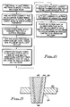
- FIGS. 3 and 4 illustrate how interconnect pads similar to that represented in FIG. 2 are processed in accordance with the present invention.
- An interconnect pad 30 having a plurality of individual tubes 34 mounted in a carrier film 32 is partially immersed in a tank 36 of molten filler 38.
- the filler 38 may be indium or a suitable solder alloy. Molten indium has a low surface energy and readily wets the copper surfaces of the tubes 34, completely filling the tubes through the mechanism of capillary action.
- the interconnect pad 32 is installed on a readout chip 44 (FIG. 4) which has a plurality of indium bumps 46 deposited on the respective contact pads. Pressure is applied to cold weld the indium filled tubes 34 to the indium bumps 46. Thereafter, an etching solution--e.g., ammonium sulphate/hydrogen peroxide for copper tubes--is applied to etch the copper away, thus freeing the polymer film carrier 32 for ready removal off the tops of the assembly of FIG. 4. This is followed by a subsequent step of attaching a detector chip 42 to the upper ends of the indium columns 40, completing the connections to the contact mesas 48, also provided with indium bumps 50. The resulting arrangement is represented schematically in FIG. 5.
- FIG. 7 is a schematic representation of the variant of the arrangement of FIG. 5 which provides additional flexibility and compliance in the final detector array assembly by virtue of the increased height of the column and its hourglass shape, achieved by abutting two indium columns together, end-to-end.
- the structure depicted in FIG. 7 is essentially like that of FIG. 5 except that two indium columns 40a and 40b are shown joined at their smaller ends 41a and 41b in an hourglass configuration.
- FIG. 8 Another variant of the invention is represented schematically in FIG. 8, whereby a pair of indium columns 40c and 40d are joined in abutment at their larger ends 51a and 51b.
- This arrangement provides the benefit of adapting indium columns 40 of a particular size to a smaller diameter contact mesa 48' and smaller contact pad 47' on the microchips 42, 44. This avoids the necessity of developing a smaller mask and smaller laser holes for the fabrication of the interconnect pad in order to match the sizes of smaller contacts on the chips 42, 44.
- it achieves the advantage of the double height indium column, similar to the arrangement of FIG. 7.
- FIG. 9 depicts the way in which an indium column may be formed from standard interconnect tubes to have an increased aspect ratio for the resulting column.
- the outer sectioned tapered cylinder 60 represents a copper tube such as 24 of FIG. 2 in the film carrier 22.
- the thickness of the cylinder 60 is typically 5 »m and the bore at the large end 62 is 15 »m.
- the inner surface of the tube 60 is plated with electroless nickel, forming a layer 64 of approximately 2 to 3 »m in thickness.
- the copper layer 60 is removed by etching and the film 22 falls off the open column ends.
- the remaining nickel tube 64 is dipped in molten indium and becomes filled with indium 66.
- the nickel tube 64 is then removed by selected etching, leaving an indium column of the form 66.
- the result is a smaller diameter column than is realized by other methods, thus providing a column with an increased aspect ratio.
- the length of the column 66 is also increased by about 50 to 100% as compared with the columns such as 40 of FIG. 5 which are produced by other methods disclosed herein.
- Arrangements in accordance with the present invention advantageously alleviate particular problems presently encountered in detector arrays operated at very cold temperatures which occur because of the effects of mismatch of the coefficients of thermal expansion of the different materials which are employed in the assembly.
- the present invention makes it possible to improve the reliability and operation of such apparatus over the multiple cool down cycles which the apparatus encounters during its operating lifetime, since the apparatus produced by the methods of the present invention is more compliant and flexible in the interconnecting columns between the respect contacts of the microchips and serves to reduce the shear forces which are encountered in the temperature cycling.
Landscapes
- Photometry And Measurement Of Optical Pulse Characteristics (AREA)
- Solid State Image Pick-Up Elements (AREA)
- Measurement Of Radiation (AREA)
- Wire Bonding (AREA)
Claims (15)
- Ein Verfahren zum Herstellen einer hybriden Detektorfeldanordnung (10) mit einem Feld von Verbindungssäulen (14), welche sich zwischen gegenüberliegenden Paaren von Kontakten von entsprechenden Detektor- (12) und Auslese-Mikrochips (14) erstrecken, welche miteinander zu verbinden sind, wobei das Verfahren die folgenden Schritte aufweist:
Bereitstellen eines Verbindungskissens (30) mit einer Mehrzahl von hohlen Metallröhren (34), die in einem Filmträger (32) angeordnet sind, wobei die Röhren (34) in einem Feld entsprechend den jeweiligen Kontaktfeldern auf den Detektor- (12) und Auslese-Mikrochips (14) angeordnet sind;
Eintauchen der Enden der Röhren (34) in ein ausgewähltes aufgeschmolzenes Füllmetall, um das Metall zu veranlassen, die Röhren durch Kapillarwirkung zu füllen; Kühlen des Verbindungskissens (30) zum Aushärten des Füllmetalls, wodurch ein Feld von Füllmetallsäulen gebildet wird, die innerhalb der Röhren (34) angeordnet sind;
Verbinden eines ersten Endes des Feldes von Füllmetallsäulen mit dem jeweiligen Feld von Kontakten auf dem Detektorchip (12) oder dem Auslesechip (14); gefolgt durch
Wegätzen der Metallröhren (34) und Entfernen des Filmträgers (32); gefolgt durch
Verbinden eines zweiten Endes des Feldes von Füllmetallsäulen mit dem jeweiligen Feld von Kontakten an dem Auslesechip (14) oder dem Detektorchip (12). - Ein Verfahren nach Anspruch 1 weiterhin mit dem Schritt des Versehens eines jeden einzelnen Kontakts des Detektor- (12) und Auslesechips (14) mit einem Indiumhöcker (46, 50), um die Verbindung einer entsprechenden Säule des Füllmetalles hiermit zu erleichtern.
- Ein Verfahren nach Anspruch 2, wobei die Füllmetallsäulen des Verbindungskissens (10) an den Indiumhöckern (46) der Kontakte des Auslesechips (14) vor dem Ätzschritt angeordnet werden.
- Ein Verfahren nach einem der vorhergehenden Ansprüche, wobei das ausgewählte Füllmetall Indium ist.
- Ein Verfahren nach einem der Ansprüche 1, 2 oder 3, wobei das ausgewählte Füllmetall eine bestimmte Lotlegierung ist.
- Ein Verfahren nach einem der vorhergehenden Ansprüche, wobei die hohlen Metallröhren (34) aus Kupfer gebildet sind.
- Ein Verfahren nach einem der vorhergehenden Ansprüche, wobei die Ätzlösung eine Ammoniumsulfatlösung ist.
- Ein Verfahren nach Anspruch 6, weiterhin mit dem Schritt des chemischen Aufbringens einer Schicht von Nickel (64) auf die innere Oberfläche der Kupferröhren (34) vor dem Schritt des Eintauchens.
- Ein Verfahren nach einem der Ansprüche 1 bis 5, wobei die hohlen Metallröhren (34) aus Nickel gebildet sind.
- Ein Verfahren nach einem der vorhergehenden Ansprüche, weiterhin mit den Schritten des Reinigens und Vorbereitens des Verbindungskissens (30) vor dem Schritt des Eintauchens.
- Ein Verfahren nach einem der vorhergehenden Ansprüche, weiterhin mit dem Schritt des Herstellens einer photoreduzierten Maske aus einem ausgewählten Detektorfeldmuster, wobei der Schritt des Bereitstellens eines Verbindungskissens (30) das Versehen eines Kissens mit einem Feld hohler Metallröhren (34) entsprechend der Maske aufweist.
- Ein Verfahren nach einem der vorhergehenden Ansprüche, wobei das Füllmetall Indium ist und die Indiumsäulen (40) sich verjüngend ausgebildet sind, und wobei das Verfahren das Bilden von zwei Feldern von Indiumsäulen aufweist, welche an ihren entsprechenden ersten Enden mit den Kontakten des Detektor- und Auslesechips verbunden sind, welche miteinander zu verbinden sind, wobei nachfolgend die freien Enden der Indiumsäulen (40) miteinander verbunden werden, um einen Abstand zwischen den Auslese- und Detektorchips in der Höhe einer doppelten Säule zu bilden.
- Ein Verfahren nach Anspruch 12, wobei die Enden kleineren Durchmessers (41a, 41b) der Indiumsäulen (40a, 40b) der entsprechenden Felder miteinander verbunden werden, um einstückige Säulen zu bilden, welche im wesentlichen sanduhrförmig sind.
- Ein Verfahren nach Anspruch 12, wobei die Enden kleineren Durchmessers der Indiumsäulen (40c, 40d) der entsprechenden Felder mit ihren zugehörigen Chipkontakten verbunden sind.
- Ein Verfahren nach Anspruch 1, wobei die hybride Detektorfeldanordnung eine Brennebenenfeld-Anordnung ist und das Verfahren die folgenden Schritte aufweist:
Verwenden des Brennebenenfeldes zur Herstellung einer photoreduzierten Maske;
Verwenden eines Verbindungskissens (30) mit Kupferröhren (34), welches der Brennebenenfeldmaske und den Spezifikationen hierfür entspricht;
Reinigen und Vorbereiten des Verbindungskissens (30) für einen Eintauchvorgang;
Eintauchen des Kissens (30) in geschmolzenes Indium und Fortfahren mit dem Tauchvorgang, bis die Röhren (34) durch Kapillarwirkung mit Indium gefüllt sind;
Übertragung der mit Indium gefüllten Röhren (34) zu dem Auslesechip (14) und Befestigen hiervon an einem Ende der individuellen Kontaktkissen (47) des Auslesechips (44) durch Kaltverschweißung der Indiumhöcker (46) an den Kissen;
Herausätzen der ursprünglichen Kupferröhren (34) mit Ammoniumsulfat, um den Trägerfilm (32) freizulegen;
Abheben des Trägerfilms (32) von dem Feld von Indiumsäulen (40); und
Anordnen des Detektorchips (42) in fluchtender Ausrichtung zu den Indiumsäulen (40) und Kaltverschweißen der oberen Enden der Säulen an Indiumhöckern (50) an den Sensorkontakten (48) durch Druckverschweißen.
Applications Claiming Priority (2)
| Application Number | Priority Date | Filing Date | Title |
|---|---|---|---|
| US37397289A | 1989-06-30 | 1989-06-30 | |
| US373972 | 1989-06-30 |
Publications (3)
| Publication Number | Publication Date |
|---|---|
| EP0405865A2 EP0405865A2 (de) | 1991-01-02 |
| EP0405865A3 EP0405865A3 (en) | 1991-06-12 |
| EP0405865B1 true EP0405865B1 (de) | 1995-04-19 |
Family
ID=23474699
Family Applications (1)
| Application Number | Title | Priority Date | Filing Date |
|---|---|---|---|
| EP90306877A Expired - Lifetime EP0405865B1 (de) | 1989-06-30 | 1990-06-22 | Verfahren zum Verbinden gegenüberliegender Paare von Detektor- und Auslesemikrochipkontakten in einer Hybriddetektoranordnung |
Country Status (7)
| Country | Link |
|---|---|
| US (1) | US5092036A (de) |
| EP (1) | EP0405865B1 (de) |
| JP (1) | JPH0770683B2 (de) |
| CA (1) | CA2017743C (de) |
| DE (1) | DE69018713T2 (de) |
| IL (1) | IL94577A (de) |
| NO (1) | NO902911L (de) |
Families Citing this family (24)
| Publication number | Priority date | Publication date | Assignee | Title |
|---|---|---|---|---|
| KR920022482A (ko) * | 1991-05-09 | 1992-12-19 | 가나이 쯔도무 | 전자부품 탑재모듈 |
| US5435037A (en) * | 1993-12-22 | 1995-07-25 | Terry R. Douglas | Paint brush with replaceable bristle pack |
| US5561593A (en) * | 1994-01-27 | 1996-10-01 | Vicon Enterprises, Inc. | Z-interface-board |
| GB9610689D0 (en) * | 1996-05-22 | 1996-07-31 | Int Computers Ltd | Flip chip attachment |
| FR2768859B1 (fr) * | 1997-09-23 | 2003-03-07 | Commissariat Energie Atomique | Systeme de composants a hybrider autorisant un defaut de planeite |
| US7026718B1 (en) | 1998-09-25 | 2006-04-11 | Stmicroelectronics, Inc. | Stacked multi-component integrated circuit microprocessor |
| US6469394B1 (en) | 2000-01-31 | 2002-10-22 | Fujitsu Limited | Conductive interconnect structures and methods for forming conductive interconnect structures |
| US20040195516A1 (en) * | 2001-02-23 | 2004-10-07 | Brian Matthews | Indium features on multi-contact chips |
| US6683375B2 (en) * | 2001-06-15 | 2004-01-27 | Fairchild Semiconductor Corporation | Semiconductor die including conductive columns |
| WO2004053443A1 (en) * | 2002-12-05 | 2004-06-24 | Bae Systems Information And Electronic Systems Integration Inc | Thermal mismatch compensation technique for integrated circuit assemblies |
| US7612443B1 (en) | 2003-09-04 | 2009-11-03 | University Of Notre Dame Du Lac | Inter-chip communication |
| US7262368B2 (en) * | 2004-08-13 | 2007-08-28 | Tessera, Inc. | Connection structures for microelectronic devices and methods for forming such structures |
| US8163644B2 (en) | 2009-10-01 | 2012-04-24 | United States Of America As Represented By The Secretary Of The Army | Template process for small pitch flip-chip interconnect hybridization |
| US8709949B2 (en) | 2011-05-13 | 2014-04-29 | Raytheon Company | System and method for removing oxide from a sensor clip assembly |
| US9620473B1 (en) | 2013-01-18 | 2017-04-11 | University Of Notre Dame Du Lac | Quilt packaging system with interdigitated interconnecting nodules for inter-chip alignment |
| US9365947B2 (en) | 2013-10-04 | 2016-06-14 | Invensas Corporation | Method for preparing low cost substrates |
| US11121302B2 (en) | 2018-10-11 | 2021-09-14 | SeeQC, Inc. | System and method for superconducting multi-chip module |
| CN110660690B (zh) * | 2019-09-29 | 2021-12-17 | 中国电子科技集团公司第十一研究所 | 红外探测器读出电路铟凸点制备方法 |
| CN111584672B (zh) * | 2020-04-23 | 2021-12-24 | 华中光电技术研究所(中国船舶重工集团公司第七一七研究所) | 一种红外焦平面探测器的铟柱及其制备方法 |
| CN116224188A (zh) * | 2023-03-13 | 2023-06-06 | 苏州大学 | 一种阵列型的霍尔芯片磁传感器及其制备方法 |
| CN116949413B (zh) * | 2023-03-16 | 2024-04-12 | 无锡中科德芯感知科技有限公司 | 铟柱制备装置、制备方法、系统、电子设备及存储介质 |
| CN117012708B (zh) * | 2023-07-03 | 2024-06-11 | 北京智创芯源科技有限公司 | 一种铟柱的制备方法及红外探测器阵列互连电路 |
| US12526920B1 (en) | 2024-01-12 | 2026-01-13 | Topline Corporation | Indium-niobium superconducting solder columns for cryogenic and quantum computer applications and methods for making same |
| CN117855340B (zh) * | 2024-03-07 | 2024-05-17 | 山西创芯光电科技有限公司 | 一种降低红外探测器盲元率的铟柱制备方法 |
Family Cites Families (16)
| Publication number | Priority date | Publication date | Assignee | Title |
|---|---|---|---|---|
| US4072863A (en) * | 1976-10-26 | 1978-02-07 | Roundy Carlos B | Pyroelectric infrared detection system |
| US4067104A (en) * | 1977-02-24 | 1978-01-10 | Rockwell International Corporation | Method of fabricating an array of flexible metallic interconnects for coupling microelectronics components |
| US4197469A (en) * | 1978-05-25 | 1980-04-08 | Rockwell International Corporation | Capacitively coupled array of photodetectors |
| US4354109A (en) * | 1979-12-31 | 1982-10-12 | Honeywell Inc. | Mounting for pyroelectric detecctor arrays |
| SE423451B (sv) * | 1980-09-15 | 1982-05-03 | Philips Svenska Ab | Sett for samarbete mellan projektiler och malfoljande projektil for genomforande av settet vid bekempning av mal |
| US4467340A (en) * | 1981-11-16 | 1984-08-21 | Rockwell International Corporation | Pre-multiplexed Schottky barrier focal plane |
| US4703559A (en) * | 1984-11-02 | 1987-11-03 | Kernforschungszentrum Karlsruhe Gmbh | Method for producing connecting elements for electrically joining microelectronic components |
| FR2577073B1 (fr) * | 1985-02-06 | 1987-09-25 | Commissariat Energie Atomique | Dispositif matriciel de detection d'un rayonnement lumineux a ecrans froids individuels integres dans un substrat et son procede de fabrication |
| CA1284523C (en) * | 1985-08-05 | 1991-05-28 | Leo G. Svendsen | Uniaxially electrically conductive articles with porous insulating substrate |
| US4670653A (en) * | 1985-10-10 | 1987-06-02 | Rockwell International Corporation | Infrared detector and imaging system |
| JPS62272564A (ja) * | 1986-05-20 | 1987-11-26 | Fujitsu Ltd | 赤外線検知装置 |
| US4740700A (en) * | 1986-09-02 | 1988-04-26 | Hughes Aircraft Company | Thermally insulative and electrically conductive interconnect and process for making same |
| JPS6413767A (en) * | 1987-07-07 | 1989-01-18 | Fujitsu Ltd | Semiconductor device |
| US4865245A (en) * | 1987-09-24 | 1989-09-12 | Santa Barbara Research Center | Oxide removal from metallic contact bumps formed on semiconductor devices to improve hybridization cold-welds |
| EP0391979A1 (de) * | 1988-02-05 | 1990-10-17 | Raychem Limited | Verwendungen von uniaxial-elektroleitenden anordnungen |
| US4862588A (en) * | 1988-07-21 | 1989-09-05 | Microelectronics And Computer Technology Corporation | Method of making a flexible interconnect |
-
1990
- 1990-05-29 CA CA002017743A patent/CA2017743C/en not_active Expired - Fee Related
- 1990-05-31 IL IL94577A patent/IL94577A/xx unknown
- 1990-06-22 DE DE69018713T patent/DE69018713T2/de not_active Expired - Lifetime
- 1990-06-22 EP EP90306877A patent/EP0405865B1/de not_active Expired - Lifetime
- 1990-06-29 JP JP2172548A patent/JPH0770683B2/ja not_active Expired - Lifetime
- 1990-06-29 NO NO90902911A patent/NO902911L/no unknown
- 1990-11-09 US US07/614,051 patent/US5092036A/en not_active Expired - Lifetime
Also Published As
| Publication number | Publication date |
|---|---|
| DE69018713D1 (de) | 1995-05-24 |
| US5092036A (en) | 1992-03-03 |
| DE69018713T2 (de) | 1995-11-16 |
| CA2017743A1 (en) | 1990-12-31 |
| IL94577A (en) | 1993-01-31 |
| IL94577A0 (en) | 1991-03-10 |
| EP0405865A2 (de) | 1991-01-02 |
| NO902911D0 (no) | 1990-06-29 |
| JPH0344955A (ja) | 1991-02-26 |
| JPH0770683B2 (ja) | 1995-07-31 |
| NO902911L (no) | 1991-01-02 |
| EP0405865A3 (en) | 1991-06-12 |
| CA2017743C (en) | 1996-02-06 |
Similar Documents
| Publication | Publication Date | Title |
|---|---|---|
| EP0405865B1 (de) | Verfahren zum Verbinden gegenüberliegender Paare von Detektor- und Auslesemikrochipkontakten in einer Hybriddetektoranordnung | |
| US6294745B1 (en) | Solder anchor decal | |
| EP0764352B1 (de) | Mikroelektronische kontakte und zusammenbauten | |
| EP0072673B1 (de) | Verdrahtungsträgerfolie für die elektrische Verbindung zwischen elektronischen Bauelementen und einer externen Schaltung | |
| US5525545A (en) | Semiconductor chip assemblies and components with pressure contact | |
| US6136047A (en) | Solder bump transfer plate | |
| US5276955A (en) | Multilayer interconnect system for an area array interconnection using solid state diffusion | |
| US7759240B2 (en) | Use of palladium in IC manufacturing with conductive polymer bump | |
| JPH10256315A (ja) | 半導体チップ付着パッドおよび形成方法 | |
| JP2002513510A (ja) | 電子デバイス用インターフェース構造 | |
| US6614110B1 (en) | Module with bumps for connection and support | |
| EP0527387B1 (de) | Verfahrungen und Vorrichtung zur Befestigung von Kontakthöckern auf TAB-Trägerleiter | |
| US5631447A (en) | Uses of uniaxially electrically conductive articles | |
| US5637925A (en) | Uses of uniaxially electrically conductive articles | |
| EP0483408B1 (de) | Auswechselbare Höchstintegrationspackung | |
| EP0171232B1 (de) | Band für die Anschweissung von Flächen | |
| US20040003496A1 (en) | Interposer to couple a microelectronic device package to a circuit board | |
| EP0440615A1 (de) | Verwendung von uniaxial leitenden gegenständen | |
| JPS6221268B2 (de) | ||
| US7371973B1 (en) | Contact node | |
| WO1999004424A1 (fr) | Dispositif a semi-conducteur, et structure de montage et procede de fabrication associes | |
| JP3267167B2 (ja) | 半導体装置とその製造方法 | |
| US20010013655A1 (en) | Methods of making microelectronic connections with liquid conductive elements |
Legal Events
| Date | Code | Title | Description |
|---|---|---|---|
| PUAI | Public reference made under article 153(3) epc to a published international application that has entered the european phase |
Free format text: ORIGINAL CODE: 0009012 |
|
| AK | Designated contracting states |
Kind code of ref document: A2 Designated state(s): CH DE FR GB IT LI NL SE |
|
| PUAL | Search report despatched |
Free format text: ORIGINAL CODE: 0009013 |
|
| AK | Designated contracting states |
Kind code of ref document: A3 Designated state(s): CH DE FR GB IT LI NL SE |
|
| 17P | Request for examination filed |
Effective date: 19911119 |
|
| 17Q | First examination report despatched |
Effective date: 19930818 |
|
| GRAA | (expected) grant |
Free format text: ORIGINAL CODE: 0009210 |
|
| AK | Designated contracting states |
Kind code of ref document: B1 Designated state(s): CH DE FR GB IT LI NL SE |
|
| REF | Corresponds to: |
Ref document number: 69018713 Country of ref document: DE Date of ref document: 19950524 |
|
| ITF | It: translation for a ep patent filed | ||
| ET | Fr: translation filed | ||
| PLBE | No opposition filed within time limit |
Free format text: ORIGINAL CODE: 0009261 |
|
| STAA | Information on the status of an ep patent application or granted ep patent |
Free format text: STATUS: NO OPPOSITION FILED WITHIN TIME LIMIT |
|
| 26N | No opposition filed | ||
| PGFP | Annual fee paid to national office [announced via postgrant information from national office to epo] |
Ref country code: SE Payment date: 19970520 Year of fee payment: 8 |
|
| PGFP | Annual fee paid to national office [announced via postgrant information from national office to epo] |
Ref country code: CH Payment date: 19970603 Year of fee payment: 8 |
|
| PG25 | Lapsed in a contracting state [announced via postgrant information from national office to epo] |
Ref country code: SE Free format text: LAPSE BECAUSE OF NON-PAYMENT OF DUE FEES Effective date: 19980623 |
|
| PG25 | Lapsed in a contracting state [announced via postgrant information from national office to epo] |
Ref country code: CH Free format text: LAPSE BECAUSE OF NON-PAYMENT OF DUE FEES Effective date: 19980630 Ref country code: LI Free format text: LAPSE BECAUSE OF NON-PAYMENT OF DUE FEES Effective date: 19980630 |
|
| REG | Reference to a national code |
Ref country code: CH Ref legal event code: PL |
|
| EUG | Se: european patent has lapsed |
Ref document number: 90306877.3 |
|
| REG | Reference to a national code |
Ref country code: GB Ref legal event code: 732E |
|
| NLS | Nl: assignments of ep-patents |
Owner name: RAYTHEON COMPANY;HE HOLDINGS, INC. |
|
| REG | Reference to a national code |
Ref country code: FR Ref legal event code: TP Ref country code: FR Ref legal event code: CA Ref country code: FR Ref legal event code: CD |
|
| REG | Reference to a national code |
Ref country code: GB Ref legal event code: IF02 |
|
| PG25 | Lapsed in a contracting state [announced via postgrant information from national office to epo] |
Ref country code: IT Free format text: LAPSE BECAUSE OF NON-PAYMENT OF DUE FEES;WARNING: LAPSES OF ITALIAN PATENTS WITH EFFECTIVE DATE BEFORE 2007 MAY HAVE OCCURRED AT ANY TIME BEFORE 2007. THE CORRECT EFFECTIVE DATE MAY BE DIFFERENT FROM THE ONE RECORDED. Effective date: 20050622 |
|
| PGFP | Annual fee paid to national office [announced via postgrant information from national office to epo] |
Ref country code: NL Payment date: 20090616 Year of fee payment: 20 |
|
| PGFP | Annual fee paid to national office [announced via postgrant information from national office to epo] |
Ref country code: FR Payment date: 20090615 Year of fee payment: 20 |
|
| PGFP | Annual fee paid to national office [announced via postgrant information from national office to epo] |
Ref country code: DE Payment date: 20090622 Year of fee payment: 20 Ref country code: GB Payment date: 20090618 Year of fee payment: 20 |
|
| REG | Reference to a national code |
Ref country code: NL Ref legal event code: V4 Effective date: 20100622 |
|
| REG | Reference to a national code |
Ref country code: GB Ref legal event code: PE20 Expiry date: 20100621 |
|
| PG25 | Lapsed in a contracting state [announced via postgrant information from national office to epo] |
Ref country code: NL Free format text: LAPSE BECAUSE OF EXPIRATION OF PROTECTION Effective date: 20100622 |
|
| PG25 | Lapsed in a contracting state [announced via postgrant information from national office to epo] |
Ref country code: GB Free format text: LAPSE BECAUSE OF EXPIRATION OF PROTECTION Effective date: 20100621 |
|
| PG25 | Lapsed in a contracting state [announced via postgrant information from national office to epo] |
Ref country code: DE Free format text: LAPSE BECAUSE OF EXPIRATION OF PROTECTION Effective date: 20100622 |