EP0405802B1 - Elektrooptischer Apparat zum Messen von ultrakurzen elektrischen Signalen - Google Patents
Elektrooptischer Apparat zum Messen von ultrakurzen elektrischen Signalen Download PDFInfo
- Publication number
- EP0405802B1 EP0405802B1 EP90306550A EP90306550A EP0405802B1 EP 0405802 B1 EP0405802 B1 EP 0405802B1 EP 90306550 A EP90306550 A EP 90306550A EP 90306550 A EP90306550 A EP 90306550A EP 0405802 B1 EP0405802 B1 EP 0405802B1
- Authority
- EP
- European Patent Office
- Prior art keywords
- quantum well
- well structure
- multiple quantum
- electrical
- electrical signal
- Prior art date
- Legal status (The legal status is an assumption and is not a legal conclusion. Google has not performed a legal analysis and makes no representation as to the accuracy of the status listed.)
- Expired - Lifetime
Links
Images

Classifications
-
- G—PHYSICS
- G01—MEASURING; TESTING
- G01R—MEASURING ELECTRIC VARIABLES; MEASURING MAGNETIC VARIABLES
- G01R31/00—Arrangements for testing electric properties; Arrangements for locating electric faults; Arrangements for electrical testing characterised by what is being tested not provided for elsewhere
- G01R31/28—Testing of electronic circuits, e.g. by signal tracer
- G01R31/302—Contactless testing
- G01R31/308—Contactless testing using non-ionising electromagnetic radiation, e.g. optical radiation
-
- G—PHYSICS
- G01—MEASURING; TESTING
- G01R—MEASURING ELECTRIC VARIABLES; MEASURING MAGNETIC VARIABLES
- G01R1/00—Details of instruments or arrangements of the types included in groups G01R5/00 - G01R13/00 and G01R31/00
- G01R1/02—General constructional details
- G01R1/06—Measuring leads; Measuring probes
- G01R1/067—Measuring probes
- G01R1/07—Non contact-making probes
- G01R1/071—Non contact-making probes containing electro-optic elements
-
- G—PHYSICS
- G01—MEASURING; TESTING
- G01R—MEASURING ELECTRIC VARIABLES; MEASURING MAGNETIC VARIABLES
- G01R15/00—Details of measuring arrangements of the types provided for in groups G01R17/00 - G01R29/00, G01R33/00 - G01R33/26 or G01R35/00
- G01R15/14—Adaptations providing voltage or current isolation, e.g. for high-voltage or high-current networks
- G01R15/24—Adaptations providing voltage or current isolation, e.g. for high-voltage or high-current networks using light-modulating devices
- G01R15/241—Adaptations providing voltage or current isolation, e.g. for high-voltage or high-current networks using light-modulating devices using electro-optical modulators, e.g. electro-absorption
-
- G—PHYSICS
- G01—MEASURING; TESTING
- G01R—MEASURING ELECTRIC VARIABLES; MEASURING MAGNETIC VARIABLES
- G01R29/00—Arrangements for measuring or indicating electric quantities not covered by groups G01R19/00 - G01R27/00
- G01R29/02—Measuring characteristics of individual pulses, e.g. deviation from pulse flatness, rise time or duration
Definitions
- This invention relates to electrooptic apparatus for measuring a characteristic of an electrical signal.
- electrooptic sampling techniques utilize ultrashort optical pulses in combination with an electrooptic phenomenon, such as photoconductivity or photoemission, to make jitter-free measurements of electrical signals which are present at internal nodes of electronic devices.
- electrooptic phenomenon such as photoconductivity or photoemission
- Two main electrooptic sampling techniques which have been developed are based on either the Pockels effect or the photoconductive effect.
- an electrical signal propagating along a pair of conductive lines is measured by directing an optical beam through an electrooptic crystal (a crystal having a high electrooptic coefficient) that is placed adjacent to the pair of lines.
- electrooptic crystal a crystal having a high electrooptic coefficient
- a field-induced birefringence in the crystal, resulting from the electrical signal changes the polarization of the optical beam as it propagates through the crystal.
- Cross polarizers in combination with photodetectors detect this change in polarization and, thus, measure electrical signal activity on the conductive pair of lines. See, for example, J. A. Valdmanis et al., IEEE Journal of Quantum Electronics, Vol. QE-22, No. 1, pp. 69-78 (1986); U.S. Patent 4,446,425; and U.S. Patent 4,618,819.
- electrooptic sampling based on the photoconductive effect utilizes two optical beams, a pump beam and a probe beam, to generate and to detect an electrical signal, respectively.
- the pump beam illuminates a first gap comprising photoconductive material between a biased transmission line and a main transmission line. Free carriers produced upon illuminating the first gap reduce the resistance of the material so that charge is transferred from the biased transmission line onto the main transmission line. This charge transfer results in an electrical signal being injected onto the main transmission line.
- the probe beam illuminates a second gap comprising photoconductive material at a delay time, t+ ⁇ , between the main transmission line and a sampling electrode. This, in turn, diverts a portion of the charge on the main transmission line onto the sampling electrode.
- the injected electrical signal can be measured without physically contacting the transmission lines. Furthermore, the injected electrical signal can be directed into an electronic device and the electronic response measured by the probe beam in a similar fashion as above. See, for example, D.H. Auston, Appl. Phys. Lett., 37(4) pp. 371-373 (1980); and U.S. Patent 4,482,863.
- electrooptic sampling techniques described above have become viable means for the measurement of ultrashort electrical signals.
- electrooptic sampling based on the pockels effect has a higher temporal resolution (300 f sec) than photoconductive techniques (2 psec)
- the former has a lower voltage sensitivity and, in practice, requires an averaging of a high number of measurements for an acceptable signal to noise ratio to be achieved.
- electrooptic apparatus for measuring a characteristic of an electrical signal, comprising a multiple quantum well structure, a first and a second electrical conductor overlying said multiple quantum well structure, electrode means for applying a fixed electrical potential across said first and second electrical conductors means for illuminating by an optical beam a region between said first and second electrical conductors that substantially includes said multiple quantum well structure, and means for injecting said electrical signal across said electrical conductors, said multiple quantum well structure being responsive to variations in amplitude of said electrical signal for modulating a characteristic of said optical beam to produce a modulated optical beam.
- electrooptic apparatus as claimed in claim 1.
- An electrooptic measuring apparatus having both high voltage sensitivity and femtosecond time resolution comprises coplanar transmission lines fabricated on a semi-insulating multiple quantum well structure.
- An electrical signal such as from a high speed electronic device, injected onto the transmission lines creates an electrical field parallel to the layer planes of the multiple quantum well structure.
- Excitonic electroabsorption by the multiple quantum well structure in response to the parallel field, changes the transmissivity of the multiple quantum well structure.
- An external light beam directed through the multiple quantum well structure is modulated, resulting from the changes in transmissivity. By detecting this modulation, a sampling of the electrical signal is achieved. Measurements indicate that the present electrooptic apparatus exhibits a comparable time resolution to instruments based on other electrooptic sampling techniques.
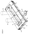
- the electrooptic apparatus comprises substantially parallel, coplanar striplines 13 and 14 (a type of coplanar transmission lines) fabricated on semi-insulating multiple quantum well structure 12. References made to a semi-insulating multiple quantum well structure is to be understood as a multiple quantum well structure comprising semiconductor material having a resistivity greater than 106 ⁇ cm.
- Coplanar striplines 13 and 14 which are electrically conductive are electrically biased at a high voltage, V bias , with respect to each other by a voltage source. Striplines 13 and 14 are long enough to insure that any electrical reflection from a terminated end of the striplines occurs at a sampling point long after the initial rise of an electrical signal.
- a bias electrical field, E bias V bias /d, is created parallel to the layer planes of multiple quantum well structure 12 by a bias voltage that is applied between striplines 13 and 14.
- multiple quantum well structure 12 has a transmissivity, T1, at photon energy 201 which corresponds to the position of its excitonic resonance peak.
- T the transmissivity
- ⁇ the absorption coefficient
- An electrical signal for example, injected from an output terminal of an electronic device onto striplines 13 and 14 produces a perturbation, E signal , in the bias electrical field.
- E signal a perturbation
- E bias +E signal a perturbed electrical field
- Excitonic electroabsorption is caused by a reduction in lifetime of excitons due to field ionization and is fully discussed in the following references: W.H. Knox et al., Appl. Phys. Lett., 48(13), pp. 864-866 (1986); and D. A. B. Miller et al., Physical Review B, 32(2), pp. 1043-1060 (1985).
- the broadening of the excitonic resonance peal due to the pea electrical field, E bias +E signal , changes the transmissivity of multiple quantum well structure 12 from T1 to T2 at photon energy 201. Therefore, an optical beam at photon energy 201 directed through multiple quantum well structure 12 experiences an optical modulation which varies in time with the amplitude of the injected electrical signal. For example, in FIG. 1, light beam 16 experiences optical modulation, (T1-T2)/T1. Furthermore, the optical modulation which can be observed in light beam 17 is due to changes in transmissiviry of multiple quantum well structure 17. Moreover, the optical modulation of light beam 17 can be processed by external circuitry such as photodetectors in combination with sampling gates to measure electrical signal activity on stripline 13 and 14.
- Conductive materials such as metals are selected for use as coplanar stripline 13 and 14. The choice of material is predicated upon factors such as resistivity and ease of fabrication, as well as other factors. Thicknesses for the striplines are chosen to be sufficient to lower the series resistance for electrical signals to propagate along the striplines. Thicknesses of the striplines must also be made in conjunction with such considerations for stripline width and interline spacing because the width and the spacing not only determine the line impedance, but also the dispersion characteristics of the striplines. Apposite to the consideration of the interline spacing is the fact that the sensitivity of the apparatus is proportional to the bias electrical field. Hence, small spacings establish higher electrical fields for a given bias voltage and, consequently, afford greater voltage sensitivity.
- the electrooptic apparatus in FIG. 1 may be fabricated, for example, by molecular beam epitaxy growth technique in conjunction with standard stripline microfabrication techniques.
- the electrooptic apparatus in FIG. 3 may be substituted for the apparatus in FIG. 1.
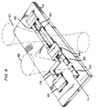
- the fabrication process is as follows. Stop etch layer 31, a 1.97 ⁇ m thickness GaAl 0.3 As 0.7 layer, is grown over a semi-insulating chromium doped GaAs substrate (not shown). Multiple quantum well structure 32 is grown on top of stop etch layer 31 and proton-implanted with 300 keV H+ ions and, then, 100 keV H+ ions.
- the energy and the dose of the implant were carefully chosen to create semi-insulating multiple quantum wells within multiple quantum well structure 32. It is extremely important that the wells be sufficiently semi-insulating to afford low power dissipation so as to prevent ohmic heating from damaging the multiple quantum wells under high electric fields.
- Proton-implantation of multiple quantum well structure 32 reduces the carrier recombination time therein to approximately 50 ps, but does not broaden the exciton resonance peak excessively.
- 10 ⁇ m wide, gold striplines 33 and 34 having a thickness of 200nm (2000 ⁇ ) and an interline spacing of 10 ⁇ m were evaporated on top of multiple quantum well structure 32.
- Multiple quantum well structure 32 comprises 50 periods of 6.93nm (69.3 ⁇ ) Al 0.32 Ga 0.68 As barrier layers and 7.225nm (72.25 ⁇ ) quantum well layers.
- the quantum well layers themselves consist of a five period superlattice: 1.15nm (11.5 ⁇ ) GaAs layers and 0.295nm (2.95 ⁇ ) Al 0.32 Ga 0.68 As layers.
- the GaAs substrate is opaque at the wavelength of interest and therefore must be removed. Using standard chemical etching techniques, the semi-insulating GaAs substrate is removed through stop etch layer 31. This effectively leaves striplines 33 and 34 free-standing on a thin film structure comprised of stop etch layer 31 and multiple quantum well structure 32.
- the thin film structure has a low effective dielectric constant (i.e.
- striplines 33 and 34 The entire structure is mounted on quartz substrate 30. Wire contacts, not shown, are placed on striplines 33 and 34 in order to facilitate applying a bias voltage parallel to the layer planes of multiple quantum well structure 32.
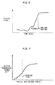
- FIG. 4 Illustrated in FIG. 4 is an example from experimental practice utilizing the electrooptic apparatus of FIG. 3 for measuring an electrical signal generated by a photoconductive switch.
- Voltage sensitivity was maximized by observing a transmission change spectrum of multiple quantum well structure 32 obtained with a bias voltage of 0 and 40 volts followed by temperature tuning the exciton resonance peak wavelength of multiple quantum well structure 32 to the wavelength of light beam 45 with a thermo-electric device.
- the temperature of multiple quantum well structure 32 was set at 5°C above ambient temperature and striplines 33 and 34 were biased at 40 volts with respect to each other to establish a bias electric field of 4 x 10⁴V cm ⁇ 1.
- the resulting short between striplines 33 and 34 generated a transient electrical signal corresponding to about a 200 mV peak signal.
- This transient signal was detected after 0.3 mm of propagation by passing weak probe beam 46 ( ⁇ .02 mW), derived from the switching beam, through multiple quantum well structure 32 and between striplines 33 and 34.
- Transmitted probe beam 47 was detected by photodetector 48 in combination with a lock-in amplifier.
- the relative intensity signal of transmitted probe beam 47 was measured at variable time delays from the start of switching beam 45. A 10%-90% risetime of 500 fs, as shown in FIG. 5, was observed after averaging ten consecutive measurements.
- FIG. 6 illustrates an exemplary embodiment of the invention for measuring the electronic response of device 606 which is fabricated on GaAs substrate 611.
- a semi-insulating multiple quantum well structure not shown, having the same structure as multiple quantum well structure 32, shown in FIG. 3, is fabricated beneath striplines 602 and 603 without supporting layers 30 and 31.
- Striplines 602 and 603 are connected to a bias voltage (not shown), and the output terminal of device 606, respectively.
- Stripline 604 is separated from stripline 605 by a gap comprising photoconductive material. When the gap between striplines 604 and 605 is illuminated by optical pulses 609, having an appropriate wavelength, photoconductivity causes an electrical signal to be injected onto stripline 605 which travels into device 606.
- the output pulse from device 606 is sampled at the output terminal by delayed optical pulse 610 illuminating a region between striplines 602 and 603 that includes a region of the semi-insulating multiple quantum well structure.
- delayed optical pulse 610 illuminating a region between striplines 602 and 603 that includes a region of the semi-insulating multiple quantum well structure.
- the electrical pulse injected into device 606 via stripline 605 may also be directly injected by another device, such as from device 607 via stripline 608. Furthermore, the electrical pulses injected onto stripline 605 may instead be a repetitive electrical signal. In this case, a repetitive electrical signal on the output terminal of device 606 will be measured.
- Devices 606 and 607 are not limited to being discrete electronic devices, but may also be integrated circuits, optoelectronic devices or the like.
- a bias voltage was applied between the coplanar striplines to set the operating point of the semi-insulating multiple quantum well structure. Defining ⁇ T as T
- V V bias - T
- V 0 , then, the relative change in transmission ⁇ T/T, indicative of the sensitivity, is highly dependent on the bias voltage as indicated by FIG. 6. Moreover, the relative transmissivity change correspondingly increases with the applied bias electrical field. Although enhanced sensitivity is achieved by a high biasing of the coplanar striplines, it should be possible to measure electrical signals with a low bias voltage. Such an operating mode, though, would reduce the voltage sensitivity of the apparatus.
- the photodetector is positioned on the same side as probe beam 47.
- GaAs/GaAlAs utilized in the above embodiments, such as InGaAs/InAlAs, InGaAs/InP and GaSb/AlGaSb, may be selected.
- femtosecond lasers operating at different wavelengths could be used as the probe beam if the layer thickness and/or material composition within the multiple quantum well structure is correspondingly adjusted in order to match the exciton resonance peak wavelength to the specific wavelength of the laser.
Landscapes
- Physics & Mathematics (AREA)
- General Physics & Mathematics (AREA)
- Engineering & Computer Science (AREA)
- Health & Medical Sciences (AREA)
- Computer Vision & Pattern Recognition (AREA)
- Electromagnetism (AREA)
- Toxicology (AREA)
- General Engineering & Computer Science (AREA)
- Light Receiving Elements (AREA)
- Measurement Of Current Or Voltage (AREA)
- Measuring Instrument Details And Bridges, And Automatic Balancing Devices (AREA)
Claims (7)
- Elektrooptische Einrichtung zum Messen einer Eigenschaft eines elektrischen Signals mit einer Mehrquantenmuldenstruktur (12); einem ersten und einem zweiten über der besagten Mehrquantenmuldenstruktur liegenden elektrischen Leiter (13 und 14); Elektrodenmitteln zum Anlegen eines festen elektrischen Potentials an besagte erste und zweite elektrische Leiter; Mitteln zum Beleuchten mit einem Lichtstrahl (16) eines Gebiets zwischen den besagten ersten und zweiten elektrischen Leitern, das im wesentlichen die besagte Mehrquantenmuldenstruktur enthält; und Mitteln zum Einkoppeln des besagten elektrischen Signals zwischen besagten elektrischen Leitern, wobei die besagte Mehrquantenmuldenstruktur auf Veränderungen der Amplitude des besagten elektrischen Signals reagiert, um eine Eigenschaft des besagten Lichtstrahls zu modulieren, um einen modulierten Lichtstrahl (17) zu erzeugen; und dadurch gekennzeichnet, daß die Quantenmuldenstruktur im wesentlichen halb-isolierendes Halbleitermaterial mit einem spezifischen Widerstand größer als 10⁶ Ωcm umfaßt und die besagten elektrischen Leiter koplanare Übertragungs leitungen sind.
- Einrichtung nach Anspruch 1, wobei die besagten koplanaren Übertragungsleitungen koplanare Streifenleitungen sind.
- Einrichtung nach Anspruch 1, wobei die besagten koplanaren Übertragungsleitungen koplanare Wellenleiter sind.
- Einrichtung nach Anspruch 1, mit Erkennungsmitteln zum Reagieren auf den besagten modulierten Lichtstrahl.
- Einrichtung nach Anspruch 4, wobei besagte Mittel zum Einkoppeln einen fotoleitenden Schalter umfassen.
- Einrichtung nach Anspruch 1, wobei besagte Mittel zum Beleuchten einen Laser zum Erzeugen des besagten Lichtstrahls umfassen.
- Einrichtung nach Anspruch 1, wobei besagte Mehrquantenmuldenstruktur besagtes Halbleitermaterial aus Verbindungen der Gruppe A₃-B₅ umfaßt, die unter den Systemen GaAs/GaAlAs, InGaAs/InP, InGaAs/InAlAs und GaSb/AlGaSb ausgewählt sind.
Applications Claiming Priority (2)
| Application Number | Priority Date | Filing Date | Title |
|---|---|---|---|
| US371475 | 1989-06-26 | ||
| US07/371,475 US4978910A (en) | 1989-06-26 | 1989-06-26 | Electrooptic apparatus for the measurement of ultrashort electrical signals |
Publications (3)
| Publication Number | Publication Date |
|---|---|
| EP0405802A2 EP0405802A2 (de) | 1991-01-02 |
| EP0405802A3 EP0405802A3 (en) | 1992-04-15 |
| EP0405802B1 true EP0405802B1 (de) | 1995-09-06 |
Family
ID=23464138
Family Applications (1)
| Application Number | Title | Priority Date | Filing Date |
|---|---|---|---|
| EP90306550A Expired - Lifetime EP0405802B1 (de) | 1989-06-26 | 1990-06-15 | Elektrooptischer Apparat zum Messen von ultrakurzen elektrischen Signalen |
Country Status (6)
| Country | Link |
|---|---|
| US (1) | US4978910A (de) |
| EP (1) | EP0405802B1 (de) |
| JP (1) | JPH0337572A (de) |
| KR (1) | KR930011425B1 (de) |
| CA (1) | CA2014681C (de) |
| DE (1) | DE69022136T2 (de) |
Cited By (1)
| Publication number | Priority date | Publication date | Assignee | Title |
|---|---|---|---|---|
| CN104297605A (zh) * | 2014-10-30 | 2015-01-21 | 云南省送变电工程公司 | 超高压带电作业绝缘安全工器具试验系统及其试验方法 |
Families Citing this family (27)
| Publication number | Priority date | Publication date | Assignee | Title |
|---|---|---|---|---|
| US4952527A (en) * | 1988-02-19 | 1990-08-28 | Massachusetts Institute Of Technology | Method of making buffer layers for III-V devices using solid phase epitaxy |
| US5332918A (en) * | 1988-02-19 | 1994-07-26 | Massachusetts Institute Of Technology | Ultra-high-speed photoconductive devices using semi-insulating layers |
| US5434698A (en) * | 1989-11-13 | 1995-07-18 | Dai Nippon Printing Co., Ltd. | Potential sensor employing electrooptic crystal and potential measuring method |
| US5262660A (en) * | 1991-08-01 | 1993-11-16 | Trw Inc. | High power pseudomorphic gallium arsenide high electron mobility transistors |
| US5635831A (en) * | 1991-12-11 | 1997-06-03 | Imatran Voima Oy | Optical voltage and electric field sensor based on the pockels effect |
| US5406194A (en) * | 1992-09-21 | 1995-04-11 | At&T Corp. | Alx Ga1-x as probe for use in electro-optic sampling |
| US5844288A (en) * | 1994-07-06 | 1998-12-01 | The Regents Of The University Of Michigan | Photoconductive element and method for measuring high frequency signals |
| US5801375A (en) * | 1995-05-23 | 1998-09-01 | Advantest Corporation | Sampler module, sampling waveform measurement device using the sample module, and sampling waveform measurement method |
| US5747791A (en) * | 1996-04-25 | 1998-05-05 | Coroy; Trenton G. | Method and devices for wavelength and power demodulation based on the use of a quantum well electroabsorption filtering detector |
| RU2117953C1 (ru) * | 1997-12-23 | 1998-08-20 | Научно-исследовательский институт импульсной техники | Устройство цифровой регистрации оптических импульсных сигналов |
| US6198580B1 (en) | 1998-08-17 | 2001-03-06 | Newport Corporation | Gimballed optical mount |
| US6516130B1 (en) | 1998-12-30 | 2003-02-04 | Newport Corporation | Clip that aligns a fiber optic cable with a laser diode within a fiber optic module |
| FR2790115B1 (fr) | 1999-02-23 | 2001-05-04 | Micro Controle | Procede et dispositif pour deplacer un mobile sur une base montee elastiquement par rapport au sol |
| US6996506B2 (en) | 1999-02-23 | 2006-02-07 | Newport Corporation | Process and device for displacing a moveable unit on a base |
| FR2791474B1 (fr) * | 1999-03-26 | 2001-06-08 | Centre Nat Rech Scient | Detecteur infrarouge semi-conducteur et son procede de fabrication |
| US6511035B1 (en) | 1999-08-03 | 2003-01-28 | Newport Corporation | Active vibration isolation systems with nonlinear compensation to account for actuator saturation |
| US6400165B1 (en) * | 2000-02-02 | 2002-06-04 | Lucent Technologies Inc. | Ultra-fast probe |
| US6655840B2 (en) | 2001-02-13 | 2003-12-02 | Newport Corporation | Stiff cross roller bearing configuration |
| US6601524B2 (en) | 2001-03-28 | 2003-08-05 | Newport Corporation | Translation table with a spring biased dovetail bearing |
| US6791058B2 (en) | 2001-04-25 | 2004-09-14 | Newport Corporation | Automatic laser weld machine for assembling photonic components |
| US6568666B2 (en) | 2001-06-13 | 2003-05-27 | Newport Corporation | Method for providing high vertical damping to pneumatic isolators during large amplitude disturbances of isolated payload |
| US6619611B2 (en) | 2001-07-02 | 2003-09-16 | Newport Corporation | Pneumatic vibration isolator utilizing an elastomeric element for isolation and attenuation of horizontal vibration |
| JP2003057118A (ja) * | 2001-07-24 | 2003-02-26 | Agilent Technol Inc | 高周波光信号測定装置 |
| US6966535B2 (en) | 2002-05-07 | 2005-11-22 | Newport Corporation | Snubber for pneumatically isolated platforms |
| US7320455B2 (en) | 2003-10-24 | 2008-01-22 | Newport Corporation | Instrumented platform for vibration-sensitive equipment |
| US8231098B2 (en) | 2004-12-07 | 2012-07-31 | Newport Corporation | Methods and devices for active vibration damping of an optical structure |
| US7929580B2 (en) * | 2006-09-22 | 2011-04-19 | Alcatel-Lucent Usa Inc. | Inexpensive terahertz pulse wave generator |
Family Cites Families (7)
| Publication number | Priority date | Publication date | Assignee | Title |
|---|---|---|---|---|
| US4482863A (en) * | 1981-08-14 | 1984-11-13 | At&T Bell Laboratories | Apparatus and method for measuring electronic response of high speed devices and materials |
| US4446425A (en) * | 1982-02-12 | 1984-05-01 | The University Of Rochester | Measurement of electrical signals with picosecond resolution |
| US4525687A (en) * | 1983-02-28 | 1985-06-25 | At&T Bell Laboratories | High speed light modulator using multiple quantum well structures |
| US4716449A (en) * | 1984-03-14 | 1987-12-29 | American Telephone And Telegraph Company At&T Bell Laboratories | Nonlinear and bistable optical device |
| US4618819A (en) * | 1984-03-27 | 1986-10-21 | The University Of Rochester | Measurement of electrical signals with subpicosecond resolution |
| US4603293A (en) * | 1984-03-27 | 1986-07-29 | University Of Rochester | Measurement of electrical signals with subpicosecond resolution |
| US4806997A (en) * | 1985-06-14 | 1989-02-21 | AT&T Laboratories American Telephone and Telegraph Company | Double heterostructure optoelectronic switch |
-
1989
- 1989-06-26 US US07/371,475 patent/US4978910A/en not_active Expired - Lifetime
-
1990
- 1990-04-17 CA CA002014681A patent/CA2014681C/en not_active Expired - Fee Related
- 1990-06-12 JP JP2151802A patent/JPH0337572A/ja active Pending
- 1990-06-15 DE DE69022136T patent/DE69022136T2/de not_active Expired - Fee Related
- 1990-06-15 EP EP90306550A patent/EP0405802B1/de not_active Expired - Lifetime
- 1990-06-21 KR KR1019900009121A patent/KR930011425B1/ko not_active Expired - Fee Related
Non-Patent Citations (2)
| Title |
|---|
| "Ultrafast Phenomena IV", eds. D.H. Auston and K.B. Eisenthal, Springer, New York, 1984, pages 406-408 * |
| NEW YORK US pages 2586 - 2595; W.H. KNOX ET AL.: 'FEMTOSECOND EXCITONIC OPTOELECTRONIS' * |
Cited By (2)
| Publication number | Priority date | Publication date | Assignee | Title |
|---|---|---|---|---|
| CN104297605A (zh) * | 2014-10-30 | 2015-01-21 | 云南省送变电工程公司 | 超高压带电作业绝缘安全工器具试验系统及其试验方法 |
| CN104297605B (zh) * | 2014-10-30 | 2017-04-19 | 云南省送变电工程公司 | 超高压带电作业绝缘安全工器具试验系统及其试验方法 |
Also Published As
| Publication number | Publication date |
|---|---|
| KR910001392A (ko) | 1991-01-30 |
| DE69022136T2 (de) | 1997-02-20 |
| CA2014681A1 (en) | 1990-12-26 |
| US4978910A (en) | 1990-12-18 |
| JPH0337572A (ja) | 1991-02-18 |
| CA2014681C (en) | 1994-10-18 |
| KR930011425B1 (ko) | 1993-12-06 |
| EP0405802A3 (en) | 1992-04-15 |
| DE69022136D1 (de) | 1995-10-12 |
| EP0405802A2 (de) | 1991-01-02 |
Similar Documents
| Publication | Publication Date | Title |
|---|---|---|
| EP0405802B1 (de) | Elektrooptischer Apparat zum Messen von ultrakurzen elektrischen Signalen | |
| Valdmanis et al. | Subpicosecond electrooptic sampling: Principles and applications | |
| Weingarten et al. | Picosecond optical sampling of GaAs integrated circuits | |
| Valdmanis | Electro-optic measurement techniques for picosecond materials, devices, and integrated circuits | |
| US5332918A (en) | Ultra-high-speed photoconductive devices using semi-insulating layers | |
| Frankel et al. | Ultrahigh-bandwidth vector network analyzer based on external electro-optic sampling | |
| Downey et al. | Picosecond dynamics of a gain-switched InGaAsP laser | |
| US4490709A (en) | InP:Fe Photoconducting device | |
| Lee et al. | Picosecond photoconductivity and its applications | |
| US6400165B1 (en) | Ultra-fast probe | |
| Zirngibl et al. | High‐speed photodetectors on InGaAs/GaAs‐on‐GaAs superlattices | |
| Hammond et al. | InP: Fe photoconductors as photodetectors | |
| Zamdmer et al. | Mode-discriminating photoconductor and coplanar waveguide circuit for picosecond sampling | |
| Schneider et al. | Diffusive electrical conduction in high‐speed p‐i‐n photodetectors | |
| Dykaar et al. | Ultrafast electrical signal generation, propagation and detection | |
| Uzorka et al. | Generation and Detection of Terahertz Electrical Waveforms | |
| Hammond et al. | InP: Fe picosecond photoconductors | |
| Jacobsen et al. | Photoconductive sampling of subpicosecond pulses using mutual inductive coupling in coplanar transmission lines | |
| Krotkus et al. | Electric field probing by picosecond laser pulses | |
| Vasil'ev et al. | Generation of picosecond electrical pulses with the aid of injection lasers | |
| Smith | Fast waveform metrology: Generation, measurement and application of sub-picosecond electrical pulses | |
| Kuhl et al. | Laser beam testing: Fast switches for generation of picosecond electrical pulses | |
| Son et al. | Photoconductive step-function sampling | |
| Hammond | Picosecond Measurements of Device and Circuit Transient Response with Optoelectric Techniques | |
| Kuhl | Contact-free characterization of electronic and optoelectronic devices with ultrashort laser pulses |
Legal Events
| Date | Code | Title | Description |
|---|---|---|---|
| PUAI | Public reference made under article 153(3) epc to a published international application that has entered the european phase |
Free format text: ORIGINAL CODE: 0009012 |
|
| AK | Designated contracting states |
Kind code of ref document: A2 Designated state(s): DE FR GB NL |
|
| PUAL | Search report despatched |
Free format text: ORIGINAL CODE: 0009013 |
|
| AK | Designated contracting states |
Kind code of ref document: A3 Designated state(s): DE FR GB NL |
|
| 17P | Request for examination filed |
Effective date: 19921002 |
|
| 17Q | First examination report despatched |
Effective date: 19940303 |
|
| RAP3 | Party data changed (applicant data changed or rights of an application transferred) |
Owner name: AT&T CORP. |
|
| GRAA | (expected) grant |
Free format text: ORIGINAL CODE: 0009210 |
|
| AK | Designated contracting states |
Kind code of ref document: B1 Designated state(s): DE FR GB NL |
|
| ET | Fr: translation filed | ||
| REF | Corresponds to: |
Ref document number: 69022136 Country of ref document: DE Date of ref document: 19951012 |
|
| PLBE | No opposition filed within time limit |
Free format text: ORIGINAL CODE: 0009261 |
|
| STAA | Information on the status of an ep patent application or granted ep patent |
Free format text: STATUS: NO OPPOSITION FILED WITHIN TIME LIMIT |
|
| 26N | No opposition filed | ||
| REG | Reference to a national code |
Ref country code: GB Ref legal event code: IF02 |
|
| PGFP | Annual fee paid to national office [announced via postgrant information from national office to epo] |
Ref country code: NL Payment date: 20080618 Year of fee payment: 19 Ref country code: DE Payment date: 20080620 Year of fee payment: 19 |
|
| PGFP | Annual fee paid to national office [announced via postgrant information from national office to epo] |
Ref country code: FR Payment date: 20080613 Year of fee payment: 19 |
|
| PGFP | Annual fee paid to national office [announced via postgrant information from national office to epo] |
Ref country code: GB Payment date: 20080620 Year of fee payment: 19 |
|
| GBPC | Gb: european patent ceased through non-payment of renewal fee |
Effective date: 20090615 |
|
| NLV4 | Nl: lapsed or anulled due to non-payment of the annual fee |
Effective date: 20100101 |
|
| REG | Reference to a national code |
Ref country code: FR Ref legal event code: ST Effective date: 20100226 |
|
| PG25 | Lapsed in a contracting state [announced via postgrant information from national office to epo] |
Ref country code: FR Free format text: LAPSE BECAUSE OF NON-PAYMENT OF DUE FEES Effective date: 20090630 |
|
| PG25 | Lapsed in a contracting state [announced via postgrant information from national office to epo] |
Ref country code: GB Free format text: LAPSE BECAUSE OF NON-PAYMENT OF DUE FEES Effective date: 20090615 |
|
| PG25 | Lapsed in a contracting state [announced via postgrant information from national office to epo] |
Ref country code: DE Free format text: LAPSE BECAUSE OF NON-PAYMENT OF DUE FEES Effective date: 20100101 |
|
| PG25 | Lapsed in a contracting state [announced via postgrant information from national office to epo] |
Ref country code: NL Free format text: LAPSE BECAUSE OF NON-PAYMENT OF DUE FEES Effective date: 20100101 |