EP0405743A2 - Zweirichtungssender-Empfänger für ein Hochgeschwindigkeitsdatensystem - Google Patents
Zweirichtungssender-Empfänger für ein Hochgeschwindigkeitsdatensystem Download PDFInfo
- Publication number
- EP0405743A2 EP0405743A2 EP90305470A EP90305470A EP0405743A2 EP 0405743 A2 EP0405743 A2 EP 0405743A2 EP 90305470 A EP90305470 A EP 90305470A EP 90305470 A EP90305470 A EP 90305470A EP 0405743 A2 EP0405743 A2 EP 0405743A2
- Authority
- EP
- European Patent Office
- Prior art keywords
- data signal
- output
- receiving
- signal
- providing
- Prior art date
- Legal status (The legal status is an assumption and is not a legal conclusion. Google has not performed a legal analysis and makes no representation as to the accuracy of the status listed.)
- Granted
Links
Images
Classifications
-
- H—ELECTRICITY
- H04—ELECTRIC COMMUNICATION TECHNIQUE
- H04B—TRANSMISSION
- H04B1/00—Details of transmission systems, not covered by a single one of groups H04B3/00 - H04B13/00; Details of transmission systems not characterised by the medium used for transmission
- H04B1/38—Transceivers, i.e. devices in which transmitter and receiver form a structural unit and in which at least one part is used for functions of transmitting and receiving
- H04B1/40—Circuits
- H04B1/54—Circuits using the same frequency for two directions of communication
- H04B1/58—Hybrid arrangements, i.e. arrangements for transition from single-path two-direction transmission to single-direction transmission on each of two paths or vice versa
- H04B1/586—Hybrid arrangements, i.e. arrangements for transition from single-path two-direction transmission to single-direction transmission on each of two paths or vice versa using an electronic circuit
-
- H—ELECTRICITY
- H04—ELECTRIC COMMUNICATION TECHNIQUE
- H04L—TRANSMISSION OF DIGITAL INFORMATION, e.g. TELEGRAPHIC COMMUNICATION
- H04L5/00—Arrangements affording multiple use of the transmission path
- H04L5/14—Two-way operation using the same type of signal, i.e. duplex
- H04L5/1423—Two-way operation using the same type of signal, i.e. duplex for simultaneous baseband signals
-
- Y—GENERAL TAGGING OF NEW TECHNOLOGICAL DEVELOPMENTS; GENERAL TAGGING OF CROSS-SECTIONAL TECHNOLOGIES SPANNING OVER SEVERAL SECTIONS OF THE IPC; TECHNICAL SUBJECTS COVERED BY FORMER USPC CROSS-REFERENCE ART COLLECTIONS [XRACs] AND DIGESTS
- Y10—TECHNICAL SUBJECTS COVERED BY FORMER USPC
- Y10S—TECHNICAL SUBJECTS COVERED BY FORMER USPC CROSS-REFERENCE ART COLLECTIONS [XRACs] AND DIGESTS
- Y10S370/00—Multiplex communications
- Y10S370/901—Wide area network
- Y10S370/902—Packet switching
- Y10S370/903—Osi compliant network
- Y10S370/906—Fiber data distribution interface, FDDI
Definitions
- the invention relates to a bidirectional transceiver for use in a high speed data transmission system. More particularly, the invention provides an alternative to fiber optic interface components for transcarrying fiber distributed data via coaxial or twisted pair media.
- the Fiber Distributed Data Interface provides a standard for high speed fiber optic data communication used in local area network applications as a high performance interconnection among mainframe computers, their mass storage sub-systems and other peripheral digital devices.
- FDDI Fiber Distributed Data Interface
- data traffic on the high speed network may approach data transmission rates of approximately 125 Megabits per second.
- the standard also requires a Bit Error rate of 2.5 X 10 ⁇ 10 which corresponds to a signal to noise ratio of about 6:1.
- FDDI compatible fiber optic components currently provide the data transmission media. While such components operate accurately and effectively, implementation of the fiber optic transmission network is costly. This cost is magnified in an office environment where numerous workstations and other digital devices are located within a relatively local geographical area. In many applications, the higher speed fiber optic network replaces an existing lower speed network operating over a coaxial or twisted pair media. Thus, the cost of implementing the fiber optic network includes the removal of the already existing network.
- coaxial components provide a cost savings on the order of twenty to one in comparison with optical components.
- Collision detection is another approach to bidirectional transmission. This approach involves biasing packets of data at a predetermined DC voltage level. The simultaneous transmission of two or more packets creates an increased DC voltage level.
- the collision detection approach requires additional collision handling algorithms that are time consuming and do not conform with the FDDI standard. Therefore, a need exists to provide a transmission media for FDDI data at a lower cost yet conforms to the requirements of the FDDI standard.
- the present invention provides inexpensive circuitry for using a single coaxial conductor or twisted pairs of wires in place of two fiber optic cables for interoperation in a Fiber Distributed Data Interface data communication network operating at high speeds.
- the invention operates reliably over distances typically less than 100 meters at frequencies of 125 megabits per second by separating supplied data signals from received data signals when both occur simultaneously over the transmission medium.
- a transceiver circuit for simultaneously receiving and supplying data over a coaxial conductor in a high speed transmission network includes a transmitter section for supplying a transmitted data signal.
- An impedance bridge network receives the transmitted data signal and a received signal and provides a cancelling signal output having a component of the transmitted data signal.
- the impedance network also provides a combined signal output including a component of the transmitted signal and the received signal.
- the transceiver circuit also includes a first equalizing circuit that receives the transmitted data signal from the transmitter section to provide an equalized transmitted data signal to the impedance network.
- a second equalizing circuit receives the received data signal from the high speed subtracting circuit to provide an equalized data signal.
- the present invention provides a low cost alternative for Fiber Distributed Data Interface (FDDI) data transmission applications in a high speed data processing network with use of a single coaxial cable or twisted pair media.
- FDDI Fiber Distributed Data Interface
- a bidirectional transceiver is disclosed that combines supplied high speed data signals with received high speed data signals when both occur simultaneously over the coaxial transcarrying media.
- the invention operates efficiently and reliably over a limited distance of coaxial cable and in an alternative embodiment, provides an interface for transmission over twisted pair media. Data may thereby be transmitted using fiber optic components or be transmitted over coaxial or twisted pair media on the high speed network.
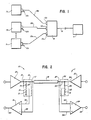
- Fig. 1 shows a high speed Fiber Distributed Data Interface (FDDI) network which operates at a data rate of approximately 125 Megabits per second.
- the network may be used in a typical office environment that is characterized by the proliferation of network nodes or workstations, shown as workstations 7a through 7n.
- Each bidirectional transceiver 10a through 10n embodying the present invention is connected to the respective workstations 7a through 7n.
- Each transceiver 10 allows the bidirectional transmission of data over a respective data transmission media such as coaxial cable 18a through 18n which is interconnected with a respective second bidirectional transceiver 11a through 11n and provides an interface with a wiring concentrator 8.
- Wiring concentrator 8 is a hub node for connection of several work stations as is well known in the field, and may, for example, operate to simultaneously receive data from and supply data to a mainframe computer 4 or other device over a fiber optic medium 6 to form part of an FDDI token ring. Wiring concentrator 8 also provides an interface between optical waves transmitted over the fiber optic medium 6 and electrical signals transmitted over the coaxial cables 18a through 18n.
- transceivers 10 and 11 provide an inexpensive alternative to the fiber optic componentry for shorter data links. Further, transceivers 10 and 11 may enable the use of already installed cable such as coaxial cable 18 in networks upgraded to run at higher speeds.
- FIG. 2 therein is shown a block diagram representation of a first coaxial transceiver 10, a coaxial data carrying cable 18, and a second coaxial transceiver 11.
- Fig. 2 illustrates one transceiver combination corresponding to each of the bidirectional transceivers 10a through 10n, coaxial cables 18a through 18n and the second bidirectional transceivers 11a through 11n shown in Fig. 1.
- Coaxial transceiver 10 includes a first transmitter 12, a first bridge network 14, and a first receiver 16.
- Transceiver 10 is coupled with a second coaxial transceiver 11 via a coaxial signal carrying conductor or cable 18.
- Second coaxial transceiver 11 includes a second transmitter 20, a second bridge network 22, and a second receiver 24.
- the first bridge network 14 is coupled with an output terminal 13 of the first transmitter section 12.
- the first bridge network 14 includes a first branch 15 comprising resistors 19 and 21 and a second branch 17 comprising a resistor 23 and the transmission line impedance of coaxial cable 18.
- the values of resistors 19, 21 and 23 are chosen to be substantially the same as the transmission line impedance of coaxial cable 18.
- the first bridge network 14 applies the signal at the output terminal 13 of first transmitter section 12 across legs 15 and 17.
- a signal equal to one half of the transmitter section output signal at terminal 13 provides a cancelling signal to one input terminal 30 of the first receiver section.
- a signal equal to one half of the transmitter section output signal at terminal 13 provides one component of a combined signal at input terminal 32 of the first receiver section.
- the first receiver section 16 subtracts the cancelling signal at terminal 30 from the combined signal at terminal 32 to provide an output at terminal 34.
- a data signal supplied by the first transmitter section 12 is thereby effectively canceled at the output terminal 34 of the first receiver section 16. This signal will appear at output terminal 34 of first receiver section 16 as a null voltage.
- a data signal supplied at the output terminal 36 of the second transmitter section 20 of transceiver 11 will likewise be applied to a second bridge network 22.
- the second bridge network 22 includes a first branch 25 comprising resistors 29 and 31 and a second branch 27 comprising a resistor 33 and the transmission line impedance of coaxial cable 18.
- the second bridge network applies the data signal supplied at the output terminal 36 from second transmitter section 20 across legs 25 and 27, providing a signal equal to one half of the second transmitter output signal to first and second input terminals of the second receiver section 24.
- the output of the second receiver section 24 provides an output voltage equal to the difference of the input signals received at terminals 38 and 40.
- the portion of the signal supplied by the second transmitter section 20 to bridge network 14 encounters a terminating impedance approximately equivalent to the value of the resistance of resistor 23 since the first transmitter section 12 appears as a low impedance.
- This signal is thereafter combined with the signal supplied by the first transmitter 12 to provide the combined signal at input terminal 32 to the first receiver section 16.
- the first receiver section 16 subtracts the cancelling signal appearing at input terminal 30 of first receiver section 16 from the combined signal appearing at input terminal 32 representing one half of the signal transmitted by first transmitter section 12 and the received signal transmitted by second transmitter section 20.
- the receiver section amplifies the difference between the signals by two and provides a resulting signal at line 34 equivalent to the signal transmitted by the second transmitter 20.
- the resulting signal on line 35 of the second receiver section 24 is an amplification of the difference of the cancelling signal supplied by the second transmitter section to input terminal 40 and the combined signal supplied by the first transmitter section 12 and the second transmitter section 20. Therefore, when the first transmitter 12 and second transmitter 20 are simultaneously transmitting data, the data supplied by the first receiver section 16 corresponds to the data supplied by the second transmitter 20 and the data supplied by the second receiver section 24 corresponds to the data supplied by the first transmitter 12.
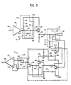
- FIG. 3 therein is shown the circuit implementation for the present invention corresponding to the first transceiver 10 shown in FIG. 2.
- ECL emitter coupled logic
- Equalizing network 40 is formed by a resistor 44, an inductor 46, a first capacitor 48, a second resistor 50, a third resistor 52 and a fourth resistor 54.
- Resistor 44 has its terminals connected between buffering output terminal 42 and terminal 56, which also provides a terminal for inductor 46 whose other terminal is connected to a positive voltage source.
- Resistor 50 has its terminals connected between terminal 42 and terminal 58 as does capacitor 48.
- Resistor 52 is connected between the positive voltage source and terminal 58 and resistor 54 has its terminals connected between terminal 58 and ground.
- the equalizing network 40 emphasizes the high frequency components and attenuates the low frequency components of the signal supplied at terminal 42. Pre-emphasis network 40 contributes to one half of the total required equalization for transceiver 10. The amount is both a function of the cable characteristics and the length. Ideally, the equalizer transfer function is the inverse of the coaxial cable's transfer function over the full operating frequency spectrum and independent of length.
- Equalizer circuit 40 Primary functions of the equalizer circuit 40 are to provide compensation for the envelope delay and amplitude distortion in the coaxial cable 18. These distortions may be defined for the media in use at a length and compensated in the equalizer circuit 40. For operation at different lengths, a nominal value may be assumed for the equalizer circuit 40. Equalization network 40 uses a pole/zero cancellation technique provided by capacitor 48 and inductor 46 to provide compensation for the zero/pole characteristic of the cable over the fundamental frequency range at a given length. Of course, different values of the components in pre-emphasis network 40 may be used to provide reliable bidirectional transmission at other lengths.
- a capacitor 60 forms part of a low pass filter including resistors 52 and 54 to limit the upper value of the high frequency components contained in the buffer output signal at terminal 42.
- the signal supplied by pre-emphasis network 40 and low pass filter is thereafter supplied to the base of a low impedance driver/emitter follower transistor 62.
- the output taken at the emitter terminal 66 of transistor 62 is capacitively coupled to the first bridge network 14 with the use of a capacitor 64.
- the first bridge network 14 comprises a first branch 15 including a first resistor 19, a second resistor 21, and a second branch including a third resistor 23, and the transmission impedance characteristic of coaxial cable 18.
- resistor 19 has its terminals connected between terminal 13 and terminal 74.
- Resistor 21 has its terminals connected between node 74 and ground.
- the second branch 17 of the bridge network 14 comprises resistor 23 having its terminals connected between terminals 13 and 75.
- Coaxial cable 18 provides the second half of the second branch 17 and has its signal carrying conductor connected to terminal 75.
- the values of resistor 19, resistor 21 and resistor 23 are chosen to be equivalent to the transmission line impedance of coaxial cable 18.
- a signal supplied by the first transmitter section 12 is applied across each resistor of branches 15 and 17 of the bridge network 14, resulting in a cancelling signal output voltage appearing at terminal 74 approximately one half of the signal at output terminal 13 from transistor 62.
- One component of a combined signal at terminal 75 corresponds to this same voltage level.
- An incoming signal supplied by coaxial cable 18 and intended to be passed by receiver 16 as data encounters an effective impedance approximately equal to the resistance of resistor 23 as its terminating impedance since the emitter follower stage of transistor 62 appears as a low impedance.
- the incoming signal provides the other component for the combined signal appearing at terminal 75.
- the cancelling signal developed at terminal 74 is thereafter applied to the base of an emitter follower transistor 78.
- the combined output signal developed at terminal 75 is applied to a matched emitter follower transistor 80.
- Transistors 78 and 80 provide buffering for the cancelling and combined signals.
- the output taken from the emitter of transistor 78 at a terminal 82 is thereafter coupled with a capacitor 84 and a resistor 86 and applied to the emitter of a single staged subtracting amplifier 90.
- the output developed at the emitter of transistor 80 is coupled to the base of transistor 90 through capacitor 92 and resistor 94.
- Transistor 90 is used as a single stage subtracting amplifier as opposed to a differential stage amplifier to reliably obtain the difference between the cancelling and the combined signals at high data transmission rates.
- the cancellation of the transmit energy in the receiver section 16 is dependent on the amplitude and phase of the signal components at the subtracting transistor 90.
- the amplitude and phase of these signals are dependent on the magnitude and phase of the impedances in the bridge network 14 including the transmission line impedance and the impedance of the emitter follower transistors 78 and 80.
- the cancelling signal and the component of the combined signal supplied by the first transmitter section 12 must be supplied to transistor 90 at the same time.
- Transistor 90 must also process the signals within a relatively short time.
- a relatively high rejection ratio for example, approximately 28 decibels (dB)
- a type 2N6604 transistor having a small capacitance between its base and collector and operative at high frequencies may be used.
- the resulting output voltage achieved at the collector of transistor 90 at terminal 96 is the difference between the cancelling signal and the combined signal.
- This output signal is again capacitively coupled to an emitter follower transistor 98 with the use of a capacitor 100.
- An emitter follower transistor 98 thereafter drives a receiver equalizing circuit 105 formed by resistor 102, a first capacitor 104 and a second capacitor 106.
- the transmitter and receiver equalizing circuits 40 and 105 when taken together, form an equalization network that compensates for the transfer function characteristic of coaxial cable 18.
- Pre-emphasis network 40 contributes to one half of the total required equalization for transceiver 10 and equalizing network 105 contributes the other half. Splitting of the equalizer into two sections reduces the level of radiated transmissions while improving the signal-to-noise ratio.
- the output of the equalizing network is then applied to a high gain comparator stage 70 and is ready for output as ECL received data.
- a data output at a line 34 indicates that the received signal is of sufficient amplitude and duration to be considered valid data. It has been found that an energy detector (not shown) of the type that is known in the art may be coupled with the output of the receiver to ensure that the transceiver is completely compatible with its fiber optic counterpart.
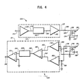
- a transceiver 100 for interfacing twisted pair media in an FDDI network includes a transmitter section 112 comprising an input buffering means 139, an equalizing circuit 140 and a second buffer 162.
- the component types, values and function of input buffering means 139, equalizing circuit 140 and second buffer 162 correspond to the input buffering means 39, the equalizing circuit 40 and the emitter/follower transistor 62 described in connection with the transmitter section 12 of Fig. 3.
- An input signal appearing as ECL coded data at input terminal 141 is provided as an output current at a line 142.
- the signal is applied to an equalizing network 140 and to the second input buffer 162 via a line 158.
- the buffer output signal at line 113 is applied through a resistor 128 whose value is chosen to match the impedance of the twisted pair and thereafter to a first input terminal of a primary winding 134 of a transformer 136.
- the second input terminal 134 of transformer 136 is connected to ground.
- the secondary winding 138 has its center grounded to obtain differential voltage signals between output terminals 130 and 132 characteristic of the ECL data signal provided to the input of the transmitter section at line 141.
- the leads of a twisted pair cable are connected to output terminals 130 and 132 and provide the transmission media for the high speed data supplied by transmitter section 112.
- Transceiver 100 also includes a receiver section 116 comprising two buffers 178 and 180, a subtracting transistor 190, an equalizing circuit 205 and an output driver 170.
- a twisted pair of conductors carrying FDDI data are applied to first and second terminals 150 and 152 of the primary winding 144 of a second transformer 146 having its center grounded.
- One output terminal 156 of the secondary winding 148 of transformer 146 develops a voltage signal across a resistor 158 that is applied to the input of buffer 180.
- Buffer 178 has its input terminal 162 grounded through a resistor 160.
- the values of resistors 158 and 160 are chosen to be the same to provide symmetrical temperature compensation and offset characteristics for buffers 178 and 180 and also to match the terminal impedance of the twisted pair transmission line.
- the output of buffer 178 is applied at a line 160 to the emitter of transistor 190.
- transceiver 100 provides ECL data at line 134 that is fully compatible with FDDI standards.
- the transceiver allows the replacement of a pair of fiber optic cables with a single coaxial cable and allows simultaneous bidirectional transmission at FDDI rates.
- a transceiver for replacing fiber optic cables with twisted pair media has been described that operates similar to the coaxial transceiver but requires two pairs of wires for bidirectional data communication.
Priority Applications (1)
| Application Number | Priority Date | Filing Date | Title |
|---|---|---|---|
| EP96200351A EP0719006A1 (de) | 1989-06-29 | 1990-05-21 | Zweirichtungssender-Empfänger für ein Hochgeschwindigkeitsdatensystem |
Applications Claiming Priority (2)
| Application Number | Priority Date | Filing Date | Title |
|---|---|---|---|
| US07/374,046 US5253249A (en) | 1989-06-29 | 1989-06-29 | Bidirectional transceiver for high speed data system |
| US374046 | 1989-06-29 |
Related Child Applications (1)
| Application Number | Title | Priority Date | Filing Date |
|---|---|---|---|
| EP96200351.3 Division-Into | 1990-05-21 |
Publications (3)
| Publication Number | Publication Date |
|---|---|
| EP0405743A2 true EP0405743A2 (de) | 1991-01-02 |
| EP0405743A3 EP0405743A3 (en) | 1992-06-03 |
| EP0405743B1 EP0405743B1 (de) | 1996-09-04 |
Family
ID=23475030
Family Applications (2)
| Application Number | Title | Priority Date | Filing Date |
|---|---|---|---|
| EP96200351A Withdrawn EP0719006A1 (de) | 1989-06-29 | 1990-05-21 | Zweirichtungssender-Empfänger für ein Hochgeschwindigkeitsdatensystem |
| EP90305470A Expired - Lifetime EP0405743B1 (de) | 1989-06-29 | 1990-05-21 | Zweirichtungssender-Empfänger für ein Hochgeschwindigkeitsdatensystem |
Family Applications Before (1)
| Application Number | Title | Priority Date | Filing Date |
|---|---|---|---|
| EP96200351A Withdrawn EP0719006A1 (de) | 1989-06-29 | 1990-05-21 | Zweirichtungssender-Empfänger für ein Hochgeschwindigkeitsdatensystem |
Country Status (4)
| Country | Link |
|---|---|
| US (2) | US5253249A (de) |
| EP (2) | EP0719006A1 (de) |
| AT (1) | ATE142393T1 (de) |
| DE (1) | DE69028356T2 (de) |
Cited By (4)
| Publication number | Priority date | Publication date | Assignee | Title |
|---|---|---|---|---|
| FR2672174A1 (fr) * | 1991-01-25 | 1992-07-31 | Alcatel Satmam | Dispositif de transmission serie en duplex integral et machine de traitement de courrier comportant un tel dispositif. |
| EP0515097A1 (de) * | 1991-05-24 | 1992-11-25 | International Business Machines Corporation | Bus-Sender/Empfänger |
| EP1006724A1 (de) * | 1993-10-20 | 2000-06-07 | Videolan Technologies, Inc. | Lokales Netzwerk für simultane Zweirichtungsübertragung von Signalen mit Videobandbreite |
| US6205170B1 (en) | 1997-03-11 | 2001-03-20 | Alcatel | Transmission/reception unit with bidirectional equalization |
Families Citing this family (60)
| Publication number | Priority date | Publication date | Assignee | Title |
|---|---|---|---|---|
| FR2674082B1 (fr) * | 1991-03-14 | 1994-11-25 | Bull Sa | Procedes de test pour transmissions serie bidirectionnelles et circuits pour leur mise en óoeuvre. |
| US5915054A (en) * | 1992-03-05 | 1999-06-22 | Fuji Xerox Co., Ltd. | Star coupler for an optical communication network |
| US5541957A (en) * | 1994-06-15 | 1996-07-30 | National Semiconductor Corporation | Apparatus for transmitting and/or receiving data at different data transfer rates especially in applications such as dual-rate ethernet local-area networks |
| US5533053A (en) * | 1994-05-16 | 1996-07-02 | Silicon Systems, Inc. | Low frequency common mode rejection in a clock circuit |
| DE4423333C1 (de) * | 1994-06-21 | 1995-08-31 | Siemens Ag | Meßeinrichtung für die U-Schnittstelle einer ISDN(Integrated Services Digital Network)-Übertragungsstrecke |
| US5491434A (en) * | 1994-12-05 | 1996-02-13 | Motorola, Inc. | Circuit and method of differential amplitude detection |
| US5822426A (en) * | 1995-06-06 | 1998-10-13 | International Business Machines Corporation | Balanced hybrid circuit |
| WO1998010590A1 (fr) * | 1996-09-02 | 1998-03-12 | Sony Corporation | Dispositif et procede de transmission d'un signal video |
| US5896417A (en) * | 1996-10-25 | 1999-04-20 | National Semiconductor Corporation | Apparatus utilizing current-to-voltage conversion for transmitting data at different data transfer rates especially in applications such as dual-rate ethernet local-area networks |
| US5801549A (en) * | 1996-12-13 | 1998-09-01 | International Business Machines Corporation | Simultaneous transmission bidirectional repeater and initialization mechanism |
| US5818874A (en) * | 1997-01-31 | 1998-10-06 | Northern Telecom Limited | Transformerless data transmission line driver |
| US5969841A (en) * | 1997-03-20 | 1999-10-19 | Methode Electronics, Inc. | Gigabaud link module with received power detect signal |
| US5977891A (en) * | 1997-09-29 | 1999-11-02 | Robert S. Turner | Base four serial communication system |
| US6480548B1 (en) | 1997-11-17 | 2002-11-12 | Silicon Graphics, Inc. | Spacial derivative bus encoder and decoder |
| US6014036A (en) * | 1997-11-20 | 2000-01-11 | International Business Machines Corporation | Bidirectional data transfer path having increased bandwidth |
| US6288813B1 (en) | 1998-03-25 | 2001-09-11 | The United States Of America As Represented By The Administrator Of The National Aeronautics And Space Administration | Apparatus and method for effecting data transfer between data systems |
| US6571393B1 (en) * | 1998-05-27 | 2003-05-27 | The Hong Kong University Of Science And Technology | Data transmission system |
| US6317464B1 (en) * | 1998-06-09 | 2001-11-13 | Nortel Networks Limited | Method and apparatus for separating digital data signals from analog voice signals transported over a common conductor |
| US6426970B1 (en) * | 1998-10-20 | 2002-07-30 | Clearcube Technology, Inc. | Bi-directional signal coupler method and apparatus |
| US6466626B1 (en) | 1999-02-23 | 2002-10-15 | International Business Machines Corporation | Driver with in-situ variable compensation for cable attenuation |
| US6775339B1 (en) | 1999-08-27 | 2004-08-10 | Silicon Graphics, Inc. | Circuit design for high-speed digital communication |
| US6218872B1 (en) * | 1999-12-23 | 2001-04-17 | Orckit Communications Ltd. | Line driver with output impedance synthesis |
| US6704277B1 (en) | 1999-12-29 | 2004-03-09 | Intel Corporation | Testing for digital signaling |
| US7031420B1 (en) * | 1999-12-30 | 2006-04-18 | Silicon Graphics, Inc. | System and method for adaptively deskewing parallel data signals relative to a clock |
| USRE41831E1 (en) | 2000-05-23 | 2010-10-19 | Marvell International Ltd. | Class B driver |
| US7194037B1 (en) | 2000-05-23 | 2007-03-20 | Marvell International Ltd. | Active replica transformer hybrid |
| US7312739B1 (en) | 2000-05-23 | 2007-12-25 | Marvell International Ltd. | Communication driver |
| US7095348B1 (en) | 2000-05-23 | 2006-08-22 | Marvell International Ltd. | Communication driver |
| US7113121B1 (en) | 2000-05-23 | 2006-09-26 | Marvell International Ltd. | Communication driver |
| US6775529B1 (en) | 2000-07-31 | 2004-08-10 | Marvell International Ltd. | Active resistive summer for a transformer hybrid |
| US7433665B1 (en) | 2000-07-31 | 2008-10-07 | Marvell International Ltd. | Apparatus and method for converting single-ended signals to a differential signal, and transceiver employing same |
| US6462688B1 (en) | 2000-12-18 | 2002-10-08 | Marvell International, Ltd. | Direct drive programmable high speed power digital-to-analog converter |
| US7606547B1 (en) | 2000-07-31 | 2009-10-20 | Marvell International Ltd. | Active resistance summer for a transformer hybrid |
| US6771675B1 (en) * | 2000-08-17 | 2004-08-03 | International Business Machines Corporation | Method for facilitating simultaneous multi-directional transmission of multiple signals between multiple circuits using a single transmission line |
| US7222208B1 (en) | 2000-08-23 | 2007-05-22 | Intel Corporation | Simultaneous bidirectional port with synchronization circuit to synchronize the port with another port |
| US6795495B2 (en) | 2000-09-25 | 2004-09-21 | Tioga Technologies, Inc. | Line driver with output impedance synthesis |
| AU2001227339A1 (en) * | 2000-10-13 | 2002-05-15 | Sharegate Inc. | Method and device for mitigating the effects of quarter-wave shorts caused by branched wiring |
| US6445170B1 (en) | 2000-10-24 | 2002-09-03 | Intel Corporation | Current source with internal variable resistance and control loop for reduced process sensitivity |
| US6728368B1 (en) * | 2000-11-06 | 2004-04-27 | Centillium Communications, Inc. | Apparatus and method for a highly efficient low power driver for a central office ADSL system |
| US6448811B1 (en) | 2001-04-02 | 2002-09-10 | Intel Corporation | Integrated circuit current reference |
| US6522174B2 (en) | 2001-04-16 | 2003-02-18 | Intel Corporation | Differential cascode current mode driver |
| US6507225B2 (en) * | 2001-04-16 | 2003-01-14 | Intel Corporation | Current mode driver with variable equalization |
| US6791356B2 (en) | 2001-06-28 | 2004-09-14 | Intel Corporation | Bidirectional port with clock channel used for synchronization |
| US6529037B1 (en) | 2001-09-13 | 2003-03-04 | Intel Corporation | Voltage mode bidirectional port with data channel used for synchronization |
| US6597198B2 (en) | 2001-10-05 | 2003-07-22 | Intel Corporation | Current mode bidirectional port with data channel used for synchronization |
| JP2003204291A (ja) * | 2002-01-07 | 2003-07-18 | Nec Corp | 通信システム |
| SE521549C2 (sv) * | 2002-03-04 | 2003-11-11 | Ericsson Telefon Ab L M | Sändare/mottagare för dubbelriktad kommunikation |
| DE60323818D1 (de) * | 2002-03-15 | 2008-11-13 | Gennum Corp | System und verfahren zum kompensieren von leitungsverlusten über eine strecke für eine digitale visuelle schnittstelle (dvi) |
| EP1552609A4 (de) * | 2002-10-08 | 2011-11-16 | Broadcom Corp | Schnelle datenverbindung mit senderentzerrung und empfängerentzerrung |
| US7606537B2 (en) * | 2004-02-10 | 2009-10-20 | Colin Dugald Brodhead | System and method for transmitting data via wave reflection |
| US7426235B1 (en) * | 2004-10-15 | 2008-09-16 | Xilinx, Inc. | Method of adaptive equalization for high-speed NRZ and multi-level signal data communications |
| US7792196B2 (en) * | 2004-12-28 | 2010-09-07 | Intel Corporation | Single conductor bidirectional communication link |
| EP1722488A1 (de) * | 2005-05-13 | 2006-11-15 | Siemens Schweiz AG | SHDSL-Übertragungsstrecke |
| US20070001704A1 (en) * | 2005-06-30 | 2007-01-04 | O'mahony Frank | Method and apparatus for equalization of connection pads |
| US7312662B1 (en) | 2005-08-09 | 2007-12-25 | Marvell International Ltd. | Cascode gain boosting system and method for a transmitter |
| US7577892B1 (en) | 2005-08-25 | 2009-08-18 | Marvell International Ltd | High speed iterative decoder |
| CN101110739B (zh) * | 2007-07-03 | 2011-03-02 | 中兴通讯股份有限公司 | 在单线对高比特率数字用户线上实现非标准低速率建链的方法 |
| US8736307B2 (en) | 2012-01-30 | 2014-05-27 | Semiconductor Components Industries, Llc | Bidirectional transceiver and method |
| US8860774B1 (en) * | 2013-06-11 | 2014-10-14 | New Vad, Llc | System and method for PC-based video conferencing and audio/video presentation |
| CN103389091A (zh) * | 2013-08-01 | 2013-11-13 | 西安应用光学研究所 | 模拟加速度计输出信号传输装置 |
Citations (4)
| Publication number | Priority date | Publication date | Assignee | Title |
|---|---|---|---|---|
| DE1512136A1 (de) * | 1967-04-01 | 1969-04-03 | Blaupunkt Werke Gmbh | Farbfernsehempfaenger mit einem Addierverstaerker |
| US3973089A (en) * | 1973-10-29 | 1976-08-03 | General Electric Company | Adaptive hybrid circuit |
| US4162371A (en) * | 1977-01-14 | 1979-07-24 | Cselt-Centro Studi E Laboratori Telecomunicazioni S.P.A. | Method of and means for establishing two-way communication between two stations interconnected by a single signal link |
| EP0211750A2 (de) * | 1985-07-31 | 1987-02-25 | AT&T Corp. | Datenübertragungssystem |
Family Cites Families (10)
| Publication number | Priority date | Publication date | Assignee | Title |
|---|---|---|---|---|
| DE1762729A1 (de) * | 1968-08-12 | 1970-10-22 | Starkstrom Anlagenbau Veb K | Logisches Grundelement zur Verknuepfung antivalent uebertragener Datensignale |
| US3725582A (en) * | 1970-12-09 | 1973-04-03 | Rca Corp | Simultaneous digital transmission in both directions over one line |
| US3730993A (en) * | 1972-01-13 | 1973-05-01 | Tektronix Inc | Transmission line circuit having common delay line for two signal paths of opposite direction |
| IT1118946B (it) * | 1979-10-04 | 1986-03-03 | Cselt Centro Studi Lab Telecom | Ricetrasmettitore per trasmissione bidirezionale simultanea di segnali numerici su una linea unica |
| JPS59221014A (ja) * | 1983-05-30 | 1984-12-12 | Sony Corp | 電圧電流変換回路 |
| US4698800A (en) * | 1985-10-28 | 1987-10-06 | International Business Machines Corporation | Bi-directional transceiver circuit |
| US5305350A (en) * | 1990-06-08 | 1994-04-19 | Chipcom Corporation | Multimedia high speed network |
| JP2520770B2 (ja) * | 1990-07-06 | 1996-07-31 | 富士通株式会社 | ハイブリッド回路 |
| US5119365A (en) * | 1990-12-14 | 1992-06-02 | Ag Communication Systems Corporation | Bi-directional buffer line amplifier |
| US5157531A (en) * | 1991-02-19 | 1992-10-20 | International Business Machines Corporation | Hybrid transmission network |
-
1989
- 1989-06-29 US US07/374,046 patent/US5253249A/en not_active Expired - Lifetime
-
1990
- 1990-05-21 EP EP96200351A patent/EP0719006A1/de not_active Withdrawn
- 1990-05-21 EP EP90305470A patent/EP0405743B1/de not_active Expired - Lifetime
- 1990-05-21 AT AT90305470T patent/ATE142393T1/de active
- 1990-05-21 DE DE69028356T patent/DE69028356T2/de not_active Expired - Fee Related
-
1995
- 1995-10-02 US US08/537,548 patent/US5579336A/en not_active Expired - Lifetime
Patent Citations (4)
| Publication number | Priority date | Publication date | Assignee | Title |
|---|---|---|---|---|
| DE1512136A1 (de) * | 1967-04-01 | 1969-04-03 | Blaupunkt Werke Gmbh | Farbfernsehempfaenger mit einem Addierverstaerker |
| US3973089A (en) * | 1973-10-29 | 1976-08-03 | General Electric Company | Adaptive hybrid circuit |
| US4162371A (en) * | 1977-01-14 | 1979-07-24 | Cselt-Centro Studi E Laboratori Telecomunicazioni S.P.A. | Method of and means for establishing two-way communication between two stations interconnected by a single signal link |
| EP0211750A2 (de) * | 1985-07-31 | 1987-02-25 | AT&T Corp. | Datenübertragungssystem |
Non-Patent Citations (2)
| Title |
|---|
| J. HECHT: 'UNDERSTANDING FIBER OPTICS', 1987, pages 375 - 381, Howard W. Sams & Co., Indianapolis, US * |
| R.W. LUCKY et al.: 'PRINCIPLES OF DATA COMMUNICATION', 1968, pages 43 - 54, McGraw-Hill, New York, US * |
Cited By (7)
| Publication number | Priority date | Publication date | Assignee | Title |
|---|---|---|---|---|
| FR2672174A1 (fr) * | 1991-01-25 | 1992-07-31 | Alcatel Satmam | Dispositif de transmission serie en duplex integral et machine de traitement de courrier comportant un tel dispositif. |
| EP0515097A1 (de) * | 1991-05-24 | 1992-11-25 | International Business Machines Corporation | Bus-Sender/Empfänger |
| US5216667A (en) * | 1991-05-24 | 1993-06-01 | International Business Machines Corporation | Simultaneous bidirectional transceiver |
| JPH05199239A (ja) * | 1991-05-24 | 1993-08-06 | Internatl Business Mach Corp <Ibm> | 同時双方向トランシーバ |
| EP1006724A1 (de) * | 1993-10-20 | 2000-06-07 | Videolan Technologies, Inc. | Lokales Netzwerk für simultane Zweirichtungsübertragung von Signalen mit Videobandbreite |
| US6240554B1 (en) | 1993-10-20 | 2001-05-29 | Igate Incorporate | Local area network for simultaneous, bi-directional transmission of video bandwidth signals |
| US6205170B1 (en) | 1997-03-11 | 2001-03-20 | Alcatel | Transmission/reception unit with bidirectional equalization |
Also Published As
| Publication number | Publication date |
|---|---|
| DE69028356D1 (de) | 1996-10-10 |
| US5579336A (en) | 1996-11-26 |
| ATE142393T1 (de) | 1996-09-15 |
| EP0719006A1 (de) | 1996-06-26 |
| EP0405743B1 (de) | 1996-09-04 |
| DE69028356T2 (de) | 1997-03-06 |
| EP0405743A3 (en) | 1992-06-03 |
| US5253249A (en) | 1993-10-12 |
Similar Documents
| Publication | Publication Date | Title |
|---|---|---|
| US5253249A (en) | Bidirectional transceiver for high speed data system | |
| US5321372A (en) | Apparatus and method for terminating cables to minimize emissions and susceptibility | |
| US6226331B1 (en) | Data access arrangement for a digital subscriber line | |
| US5465272A (en) | Data transmitter baseline wander correction circuit | |
| US3530260A (en) | Transistor hybrid circuit | |
| US7200223B2 (en) | Electronic circuit to reduce noise in digital subscriber loop and communications over unshielded twisted pair metallic conductors | |
| US7738654B2 (en) | Isolation of transmit and receive signals | |
| EP0902550A2 (de) | Netzleitungsübertragungssystem | |
| EP0560498A2 (de) | Gerät zum Zusammenstellen von breitbandigen und basisbandigen Übertragungssignalen | |
| US4688245A (en) | Method and circuit arrangement for compensating cross-talk and/or echo signals | |
| EP0773643A2 (de) | Interferenzreduktion in einem Telekommunikationssystem | |
| US7460662B2 (en) | Isolation of transmit and receive signals in full-duplex communication systems | |
| US6236726B1 (en) | Transmit power scaling for far-end crosstalk reduction | |
| JPS59225626A (ja) | デ−タ伝送装置用エコ−キヤンセラ装置 | |
| EP1000469B1 (de) | Leitungsschnittstelle für Daten- und Leistungsversorgung | |
| EP0835558B1 (de) | Datenendgerat mit verbesserter sende-empfangstrennung | |
| JPS6343444A (ja) | 多ノ−ド・バス・トポロジ−を有する局部区域ネットワ−ク | |
| JP2511598B2 (ja) | 通信システム及びトランシ―バ・モジュ―ル | |
| US6426970B1 (en) | Bi-directional signal coupler method and apparatus | |
| US6107896A (en) | Linear attenuation equalizer and method for designing same | |
| CA2356952A1 (en) | A method and apparatus for an improved analog echo canceller | |
| US6956944B1 (en) | Method and apparatus for compensating for an echo signal component in telecommunication systems | |
| US4484336A (en) | Digital transmission systems | |
| KR100325582B1 (ko) | 전화선을 통한 랜 데이터 전송장치 | |
| WO2002011377A2 (en) | Current mode transmission |
Legal Events
| Date | Code | Title | Description |
|---|---|---|---|
| PUAI | Public reference made under article 153(3) epc to a published international application that has entered the european phase |
Free format text: ORIGINAL CODE: 0009012 |
|
| 17P | Request for examination filed |
Effective date: 19900601 |
|
| AK | Designated contracting states |
Kind code of ref document: A2 Designated state(s): AT BE CH DE DK ES FR GB GR IT LI LU NL SE |
|
| PUAL | Search report despatched |
Free format text: ORIGINAL CODE: 0009013 |
|
| AK | Designated contracting states |
Kind code of ref document: A3 Designated state(s): AT BE CH DE DK ES FR GB GR IT LI LU NL SE |
|
| 16A | New documents despatched to applicant after publication of the search report | ||
| 17Q | First examination report despatched |
Effective date: 19941121 |
|
| GRAH | Despatch of communication of intention to grant a patent |
Free format text: ORIGINAL CODE: EPIDOS IGRA |
|
| GRAH | Despatch of communication of intention to grant a patent |
Free format text: ORIGINAL CODE: EPIDOS IGRA |
|
| GRAA | (expected) grant |
Free format text: ORIGINAL CODE: 0009210 |
|
| AK | Designated contracting states |
Kind code of ref document: B1 Designated state(s): AT BE CH DE DK ES FR GB GR IT LI LU NL SE |
|
| PG25 | Lapsed in a contracting state [announced via postgrant information from national office to epo] |
Ref country code: CH Effective date: 19960904 Ref country code: NL Free format text: LAPSE BECAUSE OF FAILURE TO SUBMIT A TRANSLATION OF THE DESCRIPTION OR TO PAY THE FEE WITHIN THE PRESCRIBED TIME-LIMIT Effective date: 19960904 Ref country code: LI Effective date: 19960904 Ref country code: GR Free format text: LAPSE BECAUSE OF FAILURE TO SUBMIT A TRANSLATION OF THE DESCRIPTION OR TO PAY THE FEE WITHIN THE PRESCRIBED TIME-LIMIT Effective date: 19960904 Ref country code: ES Free format text: THE PATENT HAS BEEN ANNULLED BY A DECISION OF A NATIONAL AUTHORITY Effective date: 19960904 Ref country code: DK Effective date: 19960904 Ref country code: BE Effective date: 19960904 Ref country code: AT Effective date: 19960904 |
|
| REF | Corresponds to: |
Ref document number: 142393 Country of ref document: AT Date of ref document: 19960915 Kind code of ref document: T |
|
| XX | Miscellaneous (additional remarks) |
Free format text: TEILANMELDUNG 96200351.3 EINGEREICHT AM 14/02/96. |
|
| REF | Corresponds to: |
Ref document number: 69028356 Country of ref document: DE Date of ref document: 19961010 |
|
| ITF | It: translation for a ep patent filed |
Owner name: STUDIO TORTA SOCIETA' SEMPLICE |
|
| ET | Fr: translation filed | ||
| PG25 | Lapsed in a contracting state [announced via postgrant information from national office to epo] |
Ref country code: SE Effective date: 19961204 |
|
| NLV1 | Nl: lapsed or annulled due to failure to fulfill the requirements of art. 29p and 29m of the patents act | ||
| REG | Reference to a national code |
Ref country code: CH Ref legal event code: PL |
|
| PG25 | Lapsed in a contracting state [announced via postgrant information from national office to epo] |
Ref country code: LU Free format text: LAPSE BECAUSE OF NON-PAYMENT OF DUE FEES Effective date: 19970531 |
|
| PLBE | No opposition filed within time limit |
Free format text: ORIGINAL CODE: 0009261 |
|
| STAA | Information on the status of an ep patent application or granted ep patent |
Free format text: STATUS: NO OPPOSITION FILED WITHIN TIME LIMIT |
|
| 26N | No opposition filed | ||
| PGFP | Annual fee paid to national office [announced via postgrant information from national office to epo] |
Ref country code: FR Payment date: 19980420 Year of fee payment: 9 |
|
| PGFP | Annual fee paid to national office [announced via postgrant information from national office to epo] |
Ref country code: DE Payment date: 19980421 Year of fee payment: 9 |
|
| PGFP | Annual fee paid to national office [announced via postgrant information from national office to epo] |
Ref country code: GB Payment date: 19980427 Year of fee payment: 9 |
|
| PG25 | Lapsed in a contracting state [announced via postgrant information from national office to epo] |
Ref country code: GB Free format text: LAPSE BECAUSE OF NON-PAYMENT OF DUE FEES Effective date: 19990521 |
|
| GBPC | Gb: european patent ceased through non-payment of renewal fee |
Effective date: 19990521 |
|
| PG25 | Lapsed in a contracting state [announced via postgrant information from national office to epo] |
Ref country code: FR Free format text: LAPSE BECAUSE OF NON-PAYMENT OF DUE FEES Effective date: 20000131 |
|
| PG25 | Lapsed in a contracting state [announced via postgrant information from national office to epo] |
Ref country code: DE Free format text: LAPSE BECAUSE OF NON-PAYMENT OF DUE FEES Effective date: 20000301 |
|
| REG | Reference to a national code |
Ref country code: FR Ref legal event code: ST |
|
| PG25 | Lapsed in a contracting state [announced via postgrant information from national office to epo] |
Ref country code: IT Free format text: LAPSE BECAUSE OF NON-PAYMENT OF DUE FEES;WARNING: LAPSES OF ITALIAN PATENTS WITH EFFECTIVE DATE BEFORE 2007 MAY HAVE OCCURRED AT ANY TIME BEFORE 2007. THE CORRECT EFFECTIVE DATE MAY BE DIFFERENT FROM THE ONE RECORDED. Effective date: 20050521 |
|
| PGRI | Patent reinstated in contracting state [announced from national office to epo] |
Ref country code: IT Effective date: 20091001 |
|
| PGFP | Annual fee paid to national office [announced via postgrant information from national office to epo] |
Ref country code: IT Payment date: 20060531 Year of fee payment: 17 |
|
| PGRI | Patent reinstated in contracting state [announced from national office to epo] |
Ref country code: IT Effective date: 20091001 |