EP0405587B1 - Planar interdigitated dielectric sensor - Google Patents
Planar interdigitated dielectric sensor Download PDFInfo
- Publication number
- EP0405587B1 EP0405587B1 EP90112468A EP90112468A EP0405587B1 EP 0405587 B1 EP0405587 B1 EP 0405587B1 EP 90112468 A EP90112468 A EP 90112468A EP 90112468 A EP90112468 A EP 90112468A EP 0405587 B1 EP0405587 B1 EP 0405587B1
- Authority
- EP
- European Patent Office
- Prior art keywords
- sensor
- electrode
- metallic
- planar
- dielectric
- Prior art date
- Legal status (The legal status is an assumption and is not a legal conclusion. Google has not performed a legal analysis and makes no representation as to the accuracy of the status listed.)
- Expired - Lifetime
Links
- 239000000463 material Substances 0.000 claims abstract description 28
- 230000005284 excitation Effects 0.000 claims abstract description 18
- 230000004044 response Effects 0.000 claims abstract description 17
- 239000000758 substrate Substances 0.000 claims abstract description 15
- 239000011345 viscous material Substances 0.000 claims abstract description 5
- BASFCYQUMIYNBI-UHFFFAOYSA-N platinum Chemical compound [Pt] BASFCYQUMIYNBI-UHFFFAOYSA-N 0.000 claims description 10
- 239000011521 glass Substances 0.000 claims description 5
- 229910052697 platinum Inorganic materials 0.000 claims description 5
- RYGMFSIKBFXOCR-UHFFFAOYSA-N Copper Chemical compound [Cu] RYGMFSIKBFXOCR-UHFFFAOYSA-N 0.000 claims description 2
- 229910052802 copper Inorganic materials 0.000 claims description 2
- 239000010949 copper Substances 0.000 claims description 2
- PCHJSUWPFVWCPO-UHFFFAOYSA-N gold Chemical compound [Au] PCHJSUWPFVWCPO-UHFFFAOYSA-N 0.000 claims description 2
- 229910052737 gold Inorganic materials 0.000 claims description 2
- 239000010931 gold Substances 0.000 claims description 2
- KDLHZDBZIXYQEI-UHFFFAOYSA-N Palladium Chemical compound [Pd] KDLHZDBZIXYQEI-UHFFFAOYSA-N 0.000 claims 2
- 229910052763 palladium Inorganic materials 0.000 claims 1
- 239000011810 insulating material Substances 0.000 abstract description 5
- 239000000523 sample Substances 0.000 description 25
- 238000005259 measurement Methods 0.000 description 15
- 238000000034 method Methods 0.000 description 13
- 238000004458 analytical method Methods 0.000 description 7
- 238000004519 manufacturing process Methods 0.000 description 6
- 239000000126 substance Substances 0.000 description 3
- 238000005211 surface analysis Methods 0.000 description 3
- 239000000853 adhesive Substances 0.000 description 2
- 230000001070 adhesive effect Effects 0.000 description 2
- 238000009529 body temperature measurement Methods 0.000 description 2
- 230000008859 change Effects 0.000 description 2
- 238000000576 coating method Methods 0.000 description 2
- 239000004020 conductor Substances 0.000 description 2
- 238000001816 cooling Methods 0.000 description 2
- 239000003989 dielectric material Substances 0.000 description 2
- 230000000694 effects Effects 0.000 description 2
- 238000005516 engineering process Methods 0.000 description 2
- 239000012530 fluid Substances 0.000 description 2
- 230000009477 glass transition Effects 0.000 description 2
- 229910052751 metal Inorganic materials 0.000 description 2
- 239000002184 metal Substances 0.000 description 2
- 239000000919 ceramic Substances 0.000 description 1
- 239000011248 coating agent Substances 0.000 description 1
- 210000001520 comb Anatomy 0.000 description 1
- 229920001577 copolymer Polymers 0.000 description 1
- -1 curing systems Substances 0.000 description 1
- 230000007423 decrease Effects 0.000 description 1
- 238000001514 detection method Methods 0.000 description 1
- 230000002500 effect on skin Effects 0.000 description 1
- 239000007772 electrode material Substances 0.000 description 1
- 238000005530 etching Methods 0.000 description 1
- 238000010438 heat treatment Methods 0.000 description 1
- 238000007734 materials engineering Methods 0.000 description 1
- 238000010327 methods by industry Methods 0.000 description 1
- 239000000203 mixture Substances 0.000 description 1
- 238000012544 monitoring process Methods 0.000 description 1
- 238000000465 moulding Methods 0.000 description 1
- 239000003973 paint Substances 0.000 description 1
- 230000035515 penetration Effects 0.000 description 1
- 239000004033 plastic Substances 0.000 description 1
- 229920003023 plastic Polymers 0.000 description 1
- 229920001721 polyimide Polymers 0.000 description 1
- 229920000642 polymer Polymers 0.000 description 1
- 230000008569 process Effects 0.000 description 1
- 238000007650 screen-printing Methods 0.000 description 1
Images

Classifications
-
- G—PHYSICS
- G01—MEASURING; TESTING
- G01N—INVESTIGATING OR ANALYSING MATERIALS BY DETERMINING THEIR CHEMICAL OR PHYSICAL PROPERTIES
- G01N27/00—Investigating or analysing materials by the use of electric, electrochemical, or magnetic means
- G01N27/02—Investigating or analysing materials by the use of electric, electrochemical, or magnetic means by investigating impedance
- G01N27/22—Investigating or analysing materials by the use of electric, electrochemical, or magnetic means by investigating impedance by investigating capacitance
- G01N27/226—Construction of measuring vessels; Electrodes therefor
-
- G—PHYSICS
- G01—MEASURING; TESTING
- G01R—MEASURING ELECTRIC VARIABLES; MEASURING MAGNETIC VARIABLES
- G01R27/00—Arrangements for measuring resistance, reactance, impedance, or electric characteristics derived therefrom
- G01R27/02—Measuring real or complex resistance, reactance, impedance, or other two-pole characteristics derived therefrom, e.g. time constant
- G01R27/26—Measuring inductance or capacitance; Measuring quality factor, e.g. by using the resonance method; Measuring loss factor; Measuring dielectric constants ; Measuring impedance or related variables
- G01R27/2617—Measuring dielectric properties, e.g. constants
- G01R27/2635—Sample holders, electrodes or excitation arrangements, e.g. sensors or measuring cells
Definitions
- This invention relates to a sensor which can be used to measure dielectric properties of materials.
- a device for making measurements in this manner is disclosed in copending application Serial No. 07/206,092 corresponding to EP-A-0 347 125.
- This technique is primarily used to characterize bulk properties of a material in that the signal is monitored through the entire thickness of the material. This technique has several limitations. Often times thick samples are of interest to be analyzed. In the parallel plate technique, the signal to noise ratio decreases as a function of increasing distance between the electrode plates. Larger plates could be utilized to increase the area thereby increasing the signal however there does exist a practical limitation.
- An alternate technique was developed and is commonly known which addresses the limitations of the parallel plate measurement.
- An interdigitated combed electrode is commonly used for obtaining dielectric measurements on surfaces of materials and fluids. Probes of this type have been used for many years as moisture detection devices.
- U.S. Patent No. 3,696,360 to Gajewski discloses an interdigited electrode for moisture sensing. In the past few years these interdigitated probe structures were adapted to measure dielectric properites of materials. See, Society for the Advancement of Material and Process Engineering Journal, Volume 19, No. 4, July/August, 1983.
- thermocouple is placed as close to the edge of the sample and plate as possible without contact, and the sample temperature is assumed to be that of the thermocouple. Obviously, this temperature measurement is not as accurate as measuring the temperature of the sample directly.
- thermal diode in the electrode. See, Micromet product literature in the Information Disclosue Statement - Option S-1 integrated circuit dielectric sensor for use in the Micromet Eumetric System II microdielectrometer.
- thermal diodes are limited to a temperature of 200°C and are not as accurate as temperature sensors in direct contact with the sample.
- a surface analysis dielectric sensor is needed to eliminate the above mentioned limitations of existing interdigitated pectinate probes for use with relatively viscous materials.
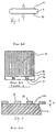
- FIG. 1 shows a typical parallel plate arrangement wherein the sample S is sandwiched between an excitation electrode plate 10 and a response electrode plate 12 .
- FIG. 2 shows a surface analysis sensor of the prior art.
- the interdigitated array 14 is made up of two combed shaped electrodes disposed in a pectinate configuration. One such electrode being the excitation electrode 18 , and the other electrode being the response electrode 19 . These electrodes are connected to electrode contacts 17 , and are supported on an insulating substrate 16 .
- FIG. 3 is a cross-section of the sensor described in FIG. 2.
- FIG. 4 shows a relatively viscous sample S′ under analysis with the sensor of FIGS. 2 and 3. As is shown, unavoidable air gaps 21 are created as the sample S′ bridges the electrode fingers 18 and 19 since the sample S′ does not readily flow.
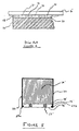
- FIG. 5 shows a top view of the sensor of the present invention. From this view it is easy to see metallic strip 26 , preferably platinum, adhered to the surface of the sensor and running around the perimeter of the sensor but not in contact with interdigitated electrode array 14′ . At the end points of metallic strip 26 are electrical contact points 27a and 27b . Metallic strip 26 serves as a resistance temperature device. It is a well known principal that by measuring the resitance of a metal, the temperature of the metal can be determined. Since metallic strip 26 is in direct contact with the sample it gives a very accurate temperature measurement of the sample.
- metallic strip 26 preferably platinum
- FIG. 5 does not show that the sensor is planar. However, this is evident from FIG. 6 which is a partial side elevational view of FIG. 5. From this view it is evident that surface 22 of the sensor is generally planar and flat. The voids between the excitation electrode 18 ′, the response electrode 19′ and metallic strip 26 contains a dielectric material 24 with known dielectric properties.
- FIG. 7 shows a sample S ⁇ under analysis with the sensor of FIG. 6. As is shown, no air gaps exist between the sensor surface and the sample being analyzed.
- the substrate 16′ of our invention is any of a number of insulating materials, well known to those skilled in the art such as polyimide film, ceramic, or glass.
- the electrodes 18′ and 19′ of our invention are metallic. As described above these electrodes are combed-shaped and disposed in a interdigitated pectinate configuration. These electrodes are attached to the upper surface of the insulating substrate 16′ .
- the electrodes 18′ and 19′ have a finite height and a flat upper surface.
- These metallic electrodes are conductors such as gold, platinum, copper, paladium, and so forth.
- metallic strip 26 also has a finite height (the same height as electrodes 18′ and 19′ ) and a flat upper surface.
- the dielectric material 24 with known dielectric properties between the electrodes is an insulating glass such as those commonly used in the manufacture of thick film hybrid circuits.
- One such insulating glass is manufactured by E.I. du Pont de Nemours and Company as thick film dielectric composition No. 5034 or No. 5042.
- Thick film hybrid technology using screen printing processes is known in the art and can be used to form the electrode array, as well as to selectively fill the spaces between the electrodes.
- a flat generally planar surface is obtained by filling the spaces between the electrodes and the resistance temperature device with excess dielectric insulating material.
- the sensor is then lapped to the desired surface flatness.
- Another method of manufacturing the sensor of the present invention utilizes etching technology. In this method grooves are etched by chemical or mechanical means into the surface of the substrate. The grooves are combed-shaped and disposed in interdigitated pectinate configuration. The grooves are then filled with the metallic conductors.
- a sensor obtained using this method is shown in FIG 7. In this configuration, the insulating material between the excitation electrode 18 ⁇ , the response electrode 19 ⁇ and metallic strip 26′ consists of the substrate 16,, itself.
Landscapes
- Physics & Mathematics (AREA)
- General Physics & Mathematics (AREA)
- Chemical & Material Sciences (AREA)
- Chemical Kinetics & Catalysis (AREA)
- Electrochemistry (AREA)
- Health & Medical Sciences (AREA)
- Life Sciences & Earth Sciences (AREA)
- Analytical Chemistry (AREA)
- Biochemistry (AREA)
- General Health & Medical Sciences (AREA)
- Immunology (AREA)
- Pathology (AREA)
- Investigating Or Analyzing Materials By The Use Of Electric Means (AREA)
- Measurement Of Resistance Or Impedance (AREA)
Abstract
Description
- This application is a continuation-in-part of application Serial No. 07/274,461 filed November 21, 1988, corresponding to US-A-5095278 and US-A-5045798.
- This invention relates to a sensor which can be used to measure dielectric properties of materials.
- It is well known that by measuring dielectric properties of a sample as a function of temperature, valuable information can be gained concerning the physical and chemical properties of the sample.
- Two techniques are commonly used to measure dielectric properties. For many years measurements have been made by placing a sample between parallel plate electrodes, applying an electrical signal in the form of an alternating voltage to one of the electrodes (i.e. the excitation electrode) and measuring the electrical signal from the other electrode (i.e. the response electrode). The following equation is used:

where
C = capacitance
eo = permitivity of free space (a constant)
e′ = permitivity of sample (being measured)
A = area of parallel plate response electrode
d = distance between the excitation and response electrode plates
By measuring capacitance, the permitivity of the sample can be easily calculated if the area of the parallel plate electrode and the distance between the excitation and response electrodes are known. A device for making measurements in this manner is disclosed in copending application Serial No. 07/206,092 corresponding to EP-A-0 347 125. This technique is primarily used to characterize bulk properties of a material in that the signal is monitored through the entire thickness of the material. This technique has several limitations. Often times thick samples are of interest to be analyzed. In the parallel plate technique, the signal to noise ratio decreases as a function of increasing distance between the electrode plates. Larger plates could be utilized to increase the area thereby increasing the signal however there does exist a practical limitation. - Many times the surface of a material is to be analyzed. In polymer molding, skin effects are of interest due to faster cooling of the materials surface than its interior. The chemical and mechanical properties of the surface of the material are more indicative of its end use properties than the bulk interior properties. Coatings on a material surface are also of interest in dielectric analysis. Paints, adhesives, and copolymers often require analysis. A parallel plate measurement would detect the properties of the coating and its associated substrate in a bulk fashion. It is impossible to analyze surface characteristics by parallel plate analysis.
- An alternate technique was developed and is commonly known which addresses the limitations of the parallel plate measurement. An interdigitated combed electrode is commonly used for obtaining dielectric measurements on surfaces of materials and fluids. Probes of this type have been used for many years as moisture detection devices. U.S. Patent No. 3,696,360 to Gajewski, discloses an interdigited electrode for moisture sensing. In the past few years these interdigitated probe structures were adapted to measure dielectric properites of materials. See, Society for the Advancement of Material and Process Engineering Journal,
Volume 19, No. 4, July/August, 1983. - In this technique a sample is placed on the electrode surface, an electrical signal is applied to one "finger" of the interdigitated fingers or combs of the electrode array, and the signal is measured at the other finger of the array. These two fingers are termed excitation and response electrodes respectively. In this fashion the signal only penetrates the surface of the material. The penetration depth is approximately equal to the distance separating the fingers in the interdigitated electrode array. This technique is ideal for monitoring the dielectric characteristics of fluids, curing systems, adhesives, and relatively low viscosity materials. This technique, however, has severe limitations when analyzing films, hard plastics, and pre-cured systems (i.e., relatively viscous materials).
- Problems arise due to surface contact with these types of materials. Interdigitated surface electrodes are inherently quite sensitive to whatever material contacts the surface, including air. Air gaps can severely limit the ability to measure dielectric properties of a material effectively since air and vacuum have the lowest permitivity theoretically possible (e′vac = 1.00000). Thus, air gaps on the electrode surface will significantly depress the measurement of a material's permittivity. Air also induces noise in the capacitance measurement. Unfortunately all electrode materials used in the fabrication of these surface sensors have a finite height or thickness. Obviously, a hard material will bridge the electrode fingers of the sensor. This bridge traps air between the electrode surface and the material in the spaces between the electrode fingers. This causes the measured permitivity to be the average value of the material's permitivity and the permittivity of air. This effect can depress the correct measurement of permitivity by as much as 50%.
- Primarily dielectric measurements are made as a function of temperature to assess the characteristics of a material. As these viscous materials are heated beyond the glass-transition region they begin to flow and displace the air between the electrode fingers. This results in a dramatic elevation in the permittivity measurement. It would seem a viable option prior to analysis to preheat materials so that they "flow out" to fill the air gaps on the electrode to address this problem. Unfortunately, most materials change their molecular structure upon heating and cooling. This change effects the accurate measurement of glass transition temperature, degree of crystallinity, degree of cure, and most importantly, permittivity. Unfortunately the amount of air present between the electrode surface and the material being analyzed changes as the material softens with temperature. If the amount of air in this space remained constant a calibration could be made and the measurement could be corrected.
- Accurate measurements of sample temperaturees obviously are also important since dielectric measurements are normally monitored as a function of temperature. In some dielectric analyzers, a thermocouple is placed as close to the edge of the sample and plate as possible without contact, and the sample temperature is assumed to be that of the thermocouple. Obviously, this temperature measurement is not as accurate as measuring the temperature of the sample directly. In at least one single surface sensor, if is known to incorporate a thermal diode in the electrode. See, Micromet product literature in the Information Disclosue Statement - Option S-1 integrated circuit dielectric sensor for use in the Micromet Eumetric System II microdielectrometer. However, thermal diodes are limited to a temperature of 200°C and are not as accurate as temperature sensors in direct contact with the sample.
- A surface analysis dielectric sensor is needed to eliminate the above mentioned limitations of existing interdigitated pectinate probes for use with relatively viscous materials.
- Provided by this invention is an surface analysis dielectric sensor according to claim 1 with the following improvements:
- (a) an interdigitated, combed electrode configuration supported on an insulating substrate;
- (b) a surface being generally planar and flat to within microns, thereby eliminating air gaps between the surface of the electrode and any material of interest; (c) an embodiment which allows accurate dielectric measurements over an extreme temperature range; and
- (d) temperature sensing means comprising a metallic strip, preferably platinum, which is adhered to the surface of the sensor.
-
- FIG. 1 is a schematic describing a parallel plate sensor configuration of the prior art with sample.
- FIG. 2 is top view of an interdigitated pectinate sensor of the prior art.
- FIG. 3 is a side elevational view of surface dielectric sensors of the prior art.
- FIG. 4 is a side elevational view which shows a sample bridging the surface sensor of the prior art.
- FIG. 5 is a top view of an interdigiated pectinate sensor of our invention.
- FIG. 6 is a side elevational view of the present invention.
- FIG. 7 is a side elevational view of a sample under analysis with the present invention.
- FIG. 8 is a side elevational view of present invention manufactured by an alternate method.
- Referring now to the drawing in FIG. 1, the schematic shows a typical parallel plate arrangement wherein the sample S is sandwiched between an
excitation electrode plate 10 and aresponse electrode plate 12. As discussed in the background, only the bulk characteristics of a material can be analyzed in this technique. FIG. 2 shows a surface analysis sensor of the prior art. The interdigitatedarray 14 is made up of two combed shaped electrodes disposed in a pectinate configuration. One such electrode being theexcitation electrode 18, and the other electrode being theresponse electrode 19. These electrodes are connected to electrodecontacts 17, and are supported on an insulatingsubstrate 16. FIG. 3 is a cross-section of the sensor described in FIG. 2. As can be readily seen theelectrodes surface 20 of thesubstate 16. FIG. 4 shows a relatively viscous sample S′ under analysis with the sensor of FIGS. 2 and 3. As is shown,unavoidable air gaps 21 are created as the sample S′ bridges theelectrode fingers - FIG. 5 shows a top view of the sensor of the present invention. From this view it is easy to see
metallic strip 26, preferably platinum, adhered to the surface of the sensor and running around the perimeter of the sensor but not in contact with interdigitatedelectrode array 14′. At the end points ofmetallic strip 26 areelectrical contact points 27a and 27b.Metallic strip 26 serves as a resistance temperature device. It is a well known principal that by measuring the resitance of a metal, the temperature of the metal can be determined. Sincemetallic strip 26 is in direct contact with the sample it gives a very accurate temperature measurement of the sample. - The view from FIG. 5 does not show that the sensor is planar. However, this is evident from FIG. 6 which is a partial side elevational view of FIG. 5. From this view it is evident that
surface 22 of the sensor is generally planar and flat. The voids between theexcitation electrode 18′, theresponse electrode 19′ andmetallic strip 26 contains adielectric material 24 with known dielectric properties. FIG. 7 shows a sample S˝ under analysis with the sensor of FIG. 6. As is shown, no air gaps exist between the sensor surface and the sample being analyzed. - The
substrate 16′ of our invention is any of a number of insulating materials, well known to those skilled in the art such as polyimide film, ceramic, or glass. Theelectrodes 18′ and 19′ of our invention are metallic. As described above these electrodes are combed-shaped and disposed in a interdigitated pectinate configuration. These electrodes are attached to the upper surface of the insulatingsubstrate 16′. Theelectrodes 18′ and 19′ have a finite height and a flat upper surface. These metallic electrodes are conductors such as gold, platinum, copper, paladium, and so forth. Likewise,metallic strip 26 also has a finite height (the same height aselectrodes 18′ and 19′) and a flat upper surface. - The
dielectric material 24 with known dielectric properties between the electrodes is an insulating glass such as those commonly used in the manufacture of thick film hybrid circuits. One such insulating glass is manufactured by E.I. du Pont de Nemours and Company as thick film dielectric composition No. 5034 or No. 5042. - There are at least two basic manufacturing methods which can be used to manufacture the sensor of the present invention. Thick film hybrid technology using screen printing processes is known in the art and can be used to form the electrode array, as well as to selectively fill the spaces between the electrodes. A flat generally planar surface is obtained by filling the spaces between the electrodes and the resistance temperature device with excess dielectric insulating material. The sensor is then lapped to the desired surface flatness. Another method of manufacturing the sensor of the present invention utilizes etching technology. In this method grooves are etched by chemical or mechanical means into the surface of the substrate. The grooves are combed-shaped and disposed in interdigitated pectinate configuration. The grooves are then filled with the metallic conductors. A sensor obtained using this method is shown in FIG 7. In this configuration, the insulating material between the
excitation electrode 18˝, theresponse electrode 19˝ andmetallic strip 26′ consists of thesubstrate 16,, itself. - Many alternate manufacturing methods would be obvious to one skilled in the art.
Claims (6)
- A planar interdigitated dielectric sensor useful for measuring surface properties of a material comprising;
an insulating substrate (16');
a metallic excitation electrode (18') attached to the surface of said substrate, the excitation electrode being comb-shaped and having a planar upper surface;
a metallic response electrode (19') attached to the surface of said substrate, the response electrode being comb-shaped, having a planar surface coplanar with said planar upper surface of the excitation electrode and interdigitatedly positioned with respect to said excitation electrode;
said planar uppers surfaces of said metallic excitation electrode (18') and of the metallic response electrode (19') forming part of a planar surface of the dielectric sensor
characterized by
a resistance temperature device (26) which is a metallic strip attached to the surface of said substrate, said metallic strip having a planar upper surface which also forms part of the surface of the dielectric sensor and
the upper surface of the dielectric sensor including the upper surfaces of the excitation electrode (18'), the response electrode (19') and the resistance temperature device (26) and being planar to such a degree that no air gaps are present between said upper surfaces and the surface of a viscous material placed against said upper surfaces. - The sensor of claim 1 wherein an insulated glass (24) with known dielectric properties is attached to the surface of the substrate (16') and fills the spaces between the excitation electrode (18'), the response electrode (19') and the metallic strip of the resistance temperature device (26).
- The sensor of claim 1 wherein the metallic excitation electrode (18''), the metallic response electrode (19'') and the metallic strip of the resistance temperature device (26') are positioned within recessed grooves of the insulating substrate (16'').
- The sensor of any one of claims 1 to 3 wherein the resistance temperature device (26, 26') is comprised of platinum.
- The sensor of any one of the preceding claims wherein the surfaces of the excitation electrode (18'), the response electrode (19'), the metallic strip (resistance temperature device 26) and the insulating glass (24) are coplanar and flat within microns.
- The sensor of any one of claims 1 to 3 wherein the electrodes (18', 19', 18'', 19'') are chosen from a group consisting of gold, platinum, copper and palladium.
Priority Applications (1)
| Application Number | Priority Date | Filing Date | Title |
|---|---|---|---|
| AT90112468T ATE104056T1 (en) | 1989-06-29 | 1990-06-29 | FLAT DIELECTRIC SENSOR IN THE FORM OF INTERLOCKING FINGERS. |
Applications Claiming Priority (2)
| Application Number | Priority Date | Filing Date | Title |
|---|---|---|---|
| US373252 | 1989-06-29 | ||
| US07/373,252 US5095278A (en) | 1988-11-21 | 1989-06-29 | Planar interdigitated dielectric sensor |
Publications (2)
| Publication Number | Publication Date |
|---|---|
| EP0405587A1 EP0405587A1 (en) | 1991-01-02 |
| EP0405587B1 true EP0405587B1 (en) | 1994-04-06 |
Family
ID=23471621
Family Applications (1)
| Application Number | Title | Priority Date | Filing Date |
|---|---|---|---|
| EP90112468A Expired - Lifetime EP0405587B1 (en) | 1989-06-29 | 1990-06-29 | Planar interdigitated dielectric sensor |
Country Status (7)
| Country | Link |
|---|---|
| US (1) | US5095278A (en) |
| EP (1) | EP0405587B1 (en) |
| JP (1) | JP2598836B2 (en) |
| AT (1) | ATE104056T1 (en) |
| CA (1) | CA2017833C (en) |
| DE (1) | DE69007872T2 (en) |
| ES (1) | ES2050888T3 (en) |
Families Citing this family (31)
| Publication number | Priority date | Publication date | Assignee | Title |
|---|---|---|---|---|
| US5208544A (en) * | 1990-09-26 | 1993-05-04 | E. I. Du Pont De Nemours And Company | Noninvasive dielectric sensor and technique for measuring polymer properties |
| US5200027A (en) * | 1991-11-12 | 1993-04-06 | General Motors Corporation | Oil microsensor having interdigitated electrodes with rough surfaces and methods of making and using the same |
| US5432435A (en) * | 1992-09-22 | 1995-07-11 | Brigham Young University | Detection of cross-linking in pre-cure stage polymeric materials by measuring their impedance |
| US5572115A (en) * | 1992-09-22 | 1996-11-05 | Brigham Young University | Device and method for measuring charge carrying activity in generally non-conductive materials |
| US5635845A (en) * | 1992-09-22 | 1997-06-03 | Brigham Young University | Detection of cross-linking in pre-cure stage polymeric materials by measuring their resistance |
| CA2080067C (en) * | 1992-10-07 | 2001-02-06 | Stuart Inkpen | Device and method for identifying and quantifying layered substances |
| US5537048A (en) * | 1994-03-14 | 1996-07-16 | Sandia Corporation | Sensing roller for in-process thickness measurement |
| US5602486A (en) * | 1994-03-14 | 1997-02-11 | Sandia Corporation | Impedance sensing of flaws in non-homogenous materials |
| US5549387A (en) * | 1994-06-01 | 1996-08-27 | The Perkin-Elmer Corporation | Apparatus and method for differential analysis using real and imaginary signal components |
| HU214533B (en) * | 1995-10-06 | 1998-03-30 | Dermo Corporation Ltd. | Detector for identifying living character of a finger |
| DE19649366C2 (en) * | 1996-11-28 | 1999-05-27 | Siemens Automotive Sa | Microsensor for liquid analysis, especially of alcohol-gasoline mixtures |
| US5907280A (en) * | 1997-04-28 | 1999-05-25 | Dkl International, Inc. | Static electrification assisted dielectrokinesis detection of plastics and other materials |
| RU2134425C1 (en) * | 1998-04-29 | 1999-08-10 | Институт физики им.Л.В.Киренского СО РАН | Pickup measuring dielectric characteristics of liquids |
| US6438497B1 (en) | 1998-12-11 | 2002-08-20 | Symyx Technologies | Method for conducting sensor array-based rapid materials characterization |
| US6535824B1 (en) | 1998-12-11 | 2003-03-18 | Symyx Technologies, Inc. | Sensor array-based system and method for rapid materials characterization |
| US6477479B1 (en) | 1998-12-11 | 2002-11-05 | Symyx Technologies | Sensor array for rapid materials characterization |
| DE10031976C2 (en) * | 2000-06-30 | 2003-11-27 | Daimler Chrysler Ag | High temperature material sensor |
| US6573734B2 (en) * | 2001-05-08 | 2003-06-03 | The Board Of Trustees Of The University Of Illinois | Integrated thin film liquid conductivity sensor |
| DE20221466U1 (en) | 2002-01-17 | 2005-12-29 | Testo Ag | Measuring assembly comprises combination of dielectric sensor and temperature sensor to determine quality of frying oil |
| DE10228811A1 (en) * | 2002-06-27 | 2004-01-29 | Fraunhofer-Gesellschaft zur Förderung der angewandten Forschung e.V. | Device for detecting a change in deposits, device for detecting a cleaning progress in a system to be cleaned and method for controlling a cleaning process of deposits on a working part |
| BRPI0313584A2 (en) | 2002-08-08 | 2016-11-08 | Sun Chemical Corp | Method and apparatus for quantitatively determining the drying rate of a liquid film |
| US7143637B1 (en) | 2003-04-11 | 2006-12-05 | Mcbrearty Michael | Dielectric slit die for in-line monitoring of liquids processing |
| WO2005055680A1 (en) * | 2003-12-05 | 2005-06-16 | The Commonwealth Of Australia | Method of manufacturing an electrical component |
| KR20090033166A (en) * | 2006-03-16 | 2009-04-01 | 알-아민 디라니 | Genetic Detection Methods and Systems |
| US7605593B2 (en) * | 2007-01-16 | 2009-10-20 | The Boeing Company | Method and apparatus for detecting inconsistencies in cured resin structures |
| ITTO20080687A1 (en) * | 2008-09-19 | 2010-03-20 | Consiglio Naz Delle Ricerche Infm Istituto | SYSTEM AND PROCEDURE FOR MEASURING DIELECTRIC PERMETTIVITY AND MAGNETIC PERMEABILITY OF A MATERIAL IN REFLECTION / TRANSMISSION. |
| DE102010050973B4 (en) | 2010-11-10 | 2019-01-24 | Thermo Electron (Karlsruhe) Gmbh | Rheometer or viscometer |
| CN107015032B (en) * | 2017-05-23 | 2023-02-24 | 河南师范大学 | Dielectric material alternating temperature testing arrangement is used in laboratory |
| DE102018220169A1 (en) | 2018-11-23 | 2020-05-28 | Infineon Technologies Ag | METHOD FOR PRODUCING A HUMIDITY SENSOR ON WAVE LEVEL AND HUMIDITY SENSOR |
| CN111721815B (en) * | 2020-06-18 | 2022-12-09 | 业成科技(成都)有限公司 | Touch device and its curing rate detection method |
| CN118549673B (en) * | 2024-05-22 | 2025-04-29 | 华中科技大学 | Dielectric sensor capable of identifying resin flowing direction and preparation method and application thereof |
Family Cites Families (13)
| Publication number | Priority date | Publication date | Assignee | Title |
|---|---|---|---|---|
| CA665303A (en) * | 1963-06-18 | Consolidated Electrodynamics Corp. | Apparatus for measuring moisture content | |
| DE1141809B (en) * | 1957-08-07 | 1962-12-27 | Max Doser Fa | Method and device for measuring the moisture content of fiber materials, e.g. B. on paper webs |
| US3706980A (en) * | 1970-04-27 | 1972-12-19 | Drexelbrook Controls | Rf system for measuring the level of materials |
| US3739266A (en) * | 1970-11-18 | 1973-06-12 | Hardwicke Etter Co | System for sensing variations in the dielectric constant of a flow of material |
| US3696360A (en) * | 1971-06-16 | 1972-10-03 | Vapor Corp | Impending condensation alarm |
| US3882381A (en) * | 1973-11-05 | 1975-05-06 | Surface Systems | System for detecting wet and icy surface conditions |
| GB1534684A (en) * | 1976-03-29 | 1978-12-06 | Secr Defence | Measuring the degree of alignment of fibres |
| US4277742A (en) * | 1977-01-31 | 1981-07-07 | Panametrics, Inc. | Absolute humidity sensors and methods of manufacturing humidity sensors |
| US4423371A (en) * | 1981-09-03 | 1983-12-27 | Massachusetts Institute Of Technology | Methods and apparatus for microdielectrometry |
| US4510436A (en) * | 1982-07-15 | 1985-04-09 | Southwest Medical Products, Incorporated | Dielectric measuring systems |
| DE3416945A1 (en) * | 1984-05-08 | 1985-11-14 | Sauter-Cumulus GmbH, 7800 Freiburg | Humidity sensor and method for fabricating it |
| US4654598A (en) * | 1985-03-08 | 1987-03-31 | The Regents Of The University Of California | Dielectric methods and apparatus for in situ prediction of porosity and specific surface area (i.e., soil type) and for detection of hydrocarbons, hazardous waste materials, and the degree of melting of ice and to predict in situ stress-strain behavior |
| US4723908A (en) * | 1985-05-01 | 1988-02-09 | Kranbuehl David E | Dielectric probe; method and apparatus including its use |
-
1989
- 1989-06-29 US US07/373,252 patent/US5095278A/en not_active Expired - Fee Related
-
1990
- 1990-05-30 CA CA002017833A patent/CA2017833C/en not_active Expired - Fee Related
- 1990-06-28 JP JP2168594A patent/JP2598836B2/en not_active Expired - Lifetime
- 1990-06-29 EP EP90112468A patent/EP0405587B1/en not_active Expired - Lifetime
- 1990-06-29 DE DE69007872T patent/DE69007872T2/en not_active Expired - Fee Related
- 1990-06-29 ES ES90112468T patent/ES2050888T3/en not_active Expired - Lifetime
- 1990-06-29 AT AT90112468T patent/ATE104056T1/en not_active IP Right Cessation
Also Published As
| Publication number | Publication date |
|---|---|
| CA2017833A1 (en) | 1990-12-29 |
| DE69007872D1 (en) | 1994-05-11 |
| DE69007872T2 (en) | 1994-11-17 |
| US5095278A (en) | 1992-03-10 |
| ES2050888T3 (en) | 1994-06-01 |
| JP2598836B2 (en) | 1997-04-09 |
| CA2017833C (en) | 1995-01-31 |
| JPH03142352A (en) | 1991-06-18 |
| EP0405587A1 (en) | 1991-01-02 |
| ATE104056T1 (en) | 1994-04-15 |
Similar Documents
| Publication | Publication Date | Title |
|---|---|---|
| US5095278A (en) | Planar interdigitated dielectric sensor | |
| US5045798A (en) | Planar interdigitated dielectric sensor | |
| US4723908A (en) | Dielectric probe; method and apparatus including its use | |
| EP0670998B1 (en) | Measurement system for monitoring the condition of polymeric materials and chemical fluids | |
| US4766369A (en) | Ice detector | |
| US4423371A (en) | Methods and apparatus for microdielectrometry | |
| JPH04501759A (en) | Equipment for measuring thermal properties of material samples | |
| CN113175948A (en) | Flexible integrated sensor and method for simultaneously measuring temperature, pressure and medium | |
| US5065106A (en) | Apparatus and method for analyzing dielectric properties using a single surface electrode and force monitoring and adjusting | |
| JPH09280911A (en) | Simultaneous measurement of pressure, strain and temperature | |
| JP7071723B2 (en) | Circuit for measuring complex permittivity, device for measuring complex permittivity, and method for measuring complex permittivity | |
| US4947131A (en) | Capacitance bar sensor | |
| US20060076644A1 (en) | Nanowire filament | |
| US6566893B2 (en) | Method and arrangement for monitoring surfaces for the presence of dew | |
| US5156045A (en) | Method related to impedance detectors in radiosondes | |
| JPH074599Y2 (en) | Sheet type sensor for permittivity measurement | |
| US20070131021A1 (en) | Capacitive vapor sensor | |
| RU1800345C (en) | Thermal-conductivity meter | |
| CA1256944A (en) | Capacitive chemical sensor using an ion exchange surface | |
| CN114487019A (en) | High-sensitivity humidity detection device based on two-dimensional material | |
| SU920361A1 (en) | Polymeric material physical parameter checking transducer | |
| EP4012393B1 (en) | Method for calibrating a fast humidity sensor | |
| SU1403740A1 (en) | Foil sensor for measuring parameters of development of surface cracks | |
| SU1670533A1 (en) | Method for determining viscosity of polymers | |
| Kang et al. | A high-speed capacitive humidity sensor |
Legal Events
| Date | Code | Title | Description |
|---|---|---|---|
| PUAI | Public reference made under article 153(3) epc to a published international application that has entered the european phase |
Free format text: ORIGINAL CODE: 0009012 |
|
| AK | Designated contracting states |
Kind code of ref document: A1 Designated state(s): AT BE CH DE DK ES FR GB GR IT LI LU NL SE |
|
| 17P | Request for examination filed |
Effective date: 19901227 |
|
| RAP1 | Party data changed (applicant data changed or rights of an application transferred) |
Owner name: TA INSTRUMENTS, INC. |
|
| 17Q | First examination report despatched |
Effective date: 19920924 |
|
| RAP3 | Party data changed (applicant data changed or rights of an application transferred) |
Owner name: TA INSTRUMENTS, INC. |
|
| GRAA | (expected) grant |
Free format text: ORIGINAL CODE: 0009210 |
|
| AK | Designated contracting states |
Kind code of ref document: B1 Designated state(s): AT BE CH DE DK ES FR GB GR IT LI LU NL SE |
|
| PG25 | Lapsed in a contracting state [announced via postgrant information from national office to epo] |
Ref country code: SE Free format text: THE PATENT HAS BEEN ANNULLED BY A DECISION OF A NATIONAL AUTHORITY Effective date: 19940406 Ref country code: GR Free format text: LAPSE BECAUSE OF FAILURE TO SUBMIT A TRANSLATION OF THE DESCRIPTION OR TO PAY THE FEE WITHIN THE PRESCRIBED TIME-LIMIT Effective date: 19940406 Ref country code: DK Effective date: 19940406 |
|
| REF | Corresponds to: |
Ref document number: 104056 Country of ref document: AT Date of ref document: 19940415 Kind code of ref document: T |
|
| REF | Corresponds to: |
Ref document number: 69007872 Country of ref document: DE Date of ref document: 19940511 |
|
| REG | Reference to a national code |
Ref country code: ES Ref legal event code: FG2A Ref document number: 2050888 Country of ref document: ES Kind code of ref document: T3 |
|
| ITF | It: translation for a ep patent filed | ||
| PG25 | Lapsed in a contracting state [announced via postgrant information from national office to epo] |
Ref country code: LU Free format text: LAPSE BECAUSE OF NON-PAYMENT OF DUE FEES Effective date: 19940630 |
|
| ET | Fr: translation filed | ||
| PLBE | No opposition filed within time limit |
Free format text: ORIGINAL CODE: 0009261 |
|
| STAA | Information on the status of an ep patent application or granted ep patent |
Free format text: STATUS: NO OPPOSITION FILED WITHIN TIME LIMIT |
|
| 26N | No opposition filed | ||
| PGFP | Annual fee paid to national office [announced via postgrant information from national office to epo] |
Ref country code: AT Payment date: 19950613 Year of fee payment: 6 |
|
| PGFP | Annual fee paid to national office [announced via postgrant information from national office to epo] |
Ref country code: ES Payment date: 19950628 Year of fee payment: 6 |
|
| ITTA | It: last paid annual fee | ||
| PG25 | Lapsed in a contracting state [announced via postgrant information from national office to epo] |
Ref country code: AT Effective date: 19960629 |
|
| PG25 | Lapsed in a contracting state [announced via postgrant information from national office to epo] |
Ref country code: ES Free format text: LAPSE BECAUSE OF THE APPLICANT RENOUNCES Effective date: 19960701 |
|
| PGFP | Annual fee paid to national office [announced via postgrant information from national office to epo] |
Ref country code: FR Payment date: 19980520 Year of fee payment: 9 |
|
| PGFP | Annual fee paid to national office [announced via postgrant information from national office to epo] |
Ref country code: GB Payment date: 19980526 Year of fee payment: 9 |
|
| PGFP | Annual fee paid to national office [announced via postgrant information from national office to epo] |
Ref country code: NL Payment date: 19980527 Year of fee payment: 9 Ref country code: DE Payment date: 19980527 Year of fee payment: 9 |
|
| PGFP | Annual fee paid to national office [announced via postgrant information from national office to epo] |
Ref country code: CH Payment date: 19980529 Year of fee payment: 9 |
|
| PGFP | Annual fee paid to national office [announced via postgrant information from national office to epo] |
Ref country code: BE Payment date: 19980615 Year of fee payment: 9 |
|
| PG25 | Lapsed in a contracting state [announced via postgrant information from national office to epo] |
Ref country code: GB Free format text: LAPSE BECAUSE OF NON-PAYMENT OF DUE FEES Effective date: 19990629 |
|
| PG25 | Lapsed in a contracting state [announced via postgrant information from national office to epo] |
Ref country code: LI Free format text: LAPSE BECAUSE OF NON-PAYMENT OF DUE FEES Effective date: 19990630 Ref country code: FR Free format text: THE PATENT HAS BEEN ANNULLED BY A DECISION OF A NATIONAL AUTHORITY Effective date: 19990630 Ref country code: CH Free format text: LAPSE BECAUSE OF NON-PAYMENT OF DUE FEES Effective date: 19990630 Ref country code: BE Free format text: LAPSE BECAUSE OF NON-PAYMENT OF DUE FEES Effective date: 19990630 |
|
| REG | Reference to a national code |
Ref country code: ES Ref legal event code: FD2A Effective date: 19991007 |
|
| BERE | Be: lapsed |
Owner name: TA INSTRUMENTS INC. Effective date: 19990630 |
|
| PG25 | Lapsed in a contracting state [announced via postgrant information from national office to epo] |
Ref country code: NL Free format text: LAPSE BECAUSE OF NON-PAYMENT OF DUE FEES Effective date: 20000101 |
|
| REG | Reference to a national code |
Ref country code: CH Ref legal event code: PL |
|
| GBPC | Gb: european patent ceased through non-payment of renewal fee |
Effective date: 19990629 |
|
| NLV4 | Nl: lapsed or anulled due to non-payment of the annual fee |
Effective date: 20000101 |
|
| PG25 | Lapsed in a contracting state [announced via postgrant information from national office to epo] |
Ref country code: DE Free format text: LAPSE BECAUSE OF NON-PAYMENT OF DUE FEES Effective date: 20000503 |
|
| REG | Reference to a national code |
Ref country code: FR Ref legal event code: ST |
|
| PG25 | Lapsed in a contracting state [announced via postgrant information from national office to epo] |
Ref country code: IT Free format text: LAPSE BECAUSE OF NON-PAYMENT OF DUE FEES;WARNING: LAPSES OF ITALIAN PATENTS WITH EFFECTIVE DATE BEFORE 2007 MAY HAVE OCCURRED AT ANY TIME BEFORE 2007. THE CORRECT EFFECTIVE DATE MAY BE DIFFERENT FROM THE ONE RECORDED. Effective date: 20050629 |