EP0403456A2 - Verschlüsselungsschaltung - Google Patents
Verschlüsselungsschaltung Download PDFInfo
- Publication number
- EP0403456A2 EP0403456A2 EP90850188A EP90850188A EP0403456A2 EP 0403456 A2 EP0403456 A2 EP 0403456A2 EP 90850188 A EP90850188 A EP 90850188A EP 90850188 A EP90850188 A EP 90850188A EP 0403456 A2 EP0403456 A2 EP 0403456A2
- Authority
- EP
- European Patent Office
- Prior art keywords
- encryption
- circuit
- memory
- bits
- data
- Prior art date
- Legal status (The legal status is an assumption and is not a legal conclusion. Google has not performed a legal analysis and makes no representation as to the accuracy of the status listed.)
- Granted
Links
Images


Classifications
-
- H—ELECTRICITY
- H04—ELECTRIC COMMUNICATION TECHNIQUE
- H04L—TRANSMISSION OF DIGITAL INFORMATION, e.g. TELEGRAPHIC COMMUNICATION
- H04L9/00—Cryptographic mechanisms or cryptographic arrangements for secret or secure communications; Network security protocols
- H04L9/06—Cryptographic mechanisms or cryptographic arrangements for secret or secure communications; Network security protocols the encryption apparatus using shift registers or memories for block-wise or stream coding, e.g. DES systems or RC4; Hash functions; Pseudorandom sequence generators
- H04L9/0618—Block ciphers, i.e. encrypting groups of characters of a plain text message using fixed encryption transformation
- H04L9/0625—Block ciphers, i.e. encrypting groups of characters of a plain text message using fixed encryption transformation with splitting of the data block into left and right halves, e.g. Feistel based algorithms, DES, FEAL, IDEA or KASUMI
-
- H—ELECTRICITY
- H04—ELECTRIC COMMUNICATION TECHNIQUE
- H04L—TRANSMISSION OF DIGITAL INFORMATION, e.g. TELEGRAPHIC COMMUNICATION
- H04L2209/00—Additional information or applications relating to cryptographic mechanisms or cryptographic arrangements for secret or secure communication H04L9/00
- H04L2209/12—Details relating to cryptographic hardware or logic circuitry
-
- H—ELECTRICITY
- H04—ELECTRIC COMMUNICATION TECHNIQUE
- H04L—TRANSMISSION OF DIGITAL INFORMATION, e.g. TELEGRAPHIC COMMUNICATION
- H04L2209/00—Additional information or applications relating to cryptographic mechanisms or cryptographic arrangements for secret or secure communication H04L9/00
- H04L2209/24—Key scheduling, i.e. generating round keys or sub-keys for block encryption
Definitions
- the invention relates to an encryption circuit constructed in gate matrix technology.
- the circuit will encrypt data according to the American DES (Data Encryption Standard).
- DES Data Encryption Standard
- NBS National Bureau of Standards
- DEA 1 DES Standard Data Encryption Algorithm No. 1
- an existing standard preferably the pin configuration of a random access memory (RAM)
- This memory circuit is produced by a number of manufacturers, for example Toshiba, whose circuit is designated PC 5564. Exchanging a memory circuit for an encryption circuit provides the possibility to communicate with encrypted data in the data system.
- the invention thus provides an encryption circuit constructed in gate matrix technology,. the circuit being integrated on a chip and the pin configuration of the circuit corresponding to the pin configuration of a memory circuit, preferably a random access memory of the standard type (RAM).
- a memory circuit preferably a random access memory of the standard type (RAM).
- the invention provides an encryption circuit in gate matrix technology. It should be able to carry put encryption and decryption according to the DES standard in the so-called ECB mode.
- the encryption algorithm is described in greater detail below.
- a main aim of the invention is that the encryption circuit shall be exchangeable for an 8 kbyte random access memory of a standard type, such as Toshiba 5564 or corresponding circuit. This is a memory circuit which is frequently used in electronic equipment. Other designations are, for example, 2064, 6264, 4364 and 8264.
- That the encryption circuit should be exchangeable implies that the electrical connections correspond to the specification of the memory circuit.
- the pin arrangement must correspond and the responses on reading and writing should occur equivalently.
- the encryption circuit should be designed in such a manner that the original 8 kbyte block is retained to the greatest possible extent. It may be difficult to meet the requirement with an internal memory in the same circuit. In this case, a decoding logic will be included for a future such memory, internally or externally. The circuit will thus generate the CS, Chip Select, signal which can be used by an internal RAM.
- CS shall be taken to pin 1 of the encryption circuit for any "piggy-back" coupling. A memory circuit is therefore soldered above or under the encryption circuit and take this CS signal from pin 1. Pin 1 is not used by the memory circuit and thus becomes an output for the encryption circuit. In many applications, the loss of a memory circuit does not play a large role.
- the encryption part will occupy a suitable number of memory cells from the highest address and downward.
- FIG. 1 shows such a system in which a memory and CPU block and colummunication block can be seen.
- rutines for data flow must naturally be modified.
- the normal data flow to communication circuits is then diverted so that data take the path via the encryption circuit.
- a hardware circuit carries out the encryption extremely quickly with the consequence that the data rate is not appreciably retarded.
- FIG. 2 shows an example of such a circuit, Toshiba 5564.
- the memory which is for 8 kbytes and has 28 pins is quite usual in systems.
- DES Data Encryption Standard
- the algorithm is intended to be implemented in hardware. Encryption and decryption are carried out equally easily with a relatively small transposition in the logic. According to the standard, there are four different ways for encrypting/decrypting: ECB Electronic Code Book, CBS Cipher Block Chaining, CFB Cipher Feedback and OFB Output Feedback.
- the first basic variant is called ECB. This is where the encryption/decryption itself is carried out.
- the other variants require ECB as a basis. CBC, CFB and OFB all use ECB plus additional logic such as EXOR gates and shift registers for achieving their specific characteristics.
- a number of circuits with the DES algorithm are found on the market, for example Motorola MC6859, Zilog Z8068 and so forth.
- the embodiment of the invention described here contains only the fundamental ECB but, naturally, the other variants can also be constructed by an expert.
- ECB encrypts 64-bit data block by block with a key of 64 bits.
- Figure 3 shows diagrammatically the encrypting operation.
- a block m of plain text is encrypted with the aid of a key. Since the encryption algorithm itself if well known, it is only the 'key which will be kept secret by the user.
- the key also consists of 64 bits but has 8 parity bits which are not included in the algorithm. 56 bits remain for the key.
- the result of the encryption is an encrypted block of 64 bits.
- the decryption follows the same principle as the encryption by transposition of so-called sub-keys. The sub-keys are calculated with the aid of the key.
- ECB is a translation table for a data word of 64 bits and a key of 5Bbits.
- Figure 4 shows a flow diagram for the data flow during encryption.
- the left block obtains the previous value from the right block.
- the right block gets new values through the exor function on the left block and a function f.
- the function f is performed with a right block and a sub-key value K; as input signals.
- the sub-keys K will be described later.
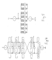
- Figure 5 shows how the function f is calculated.
- the buses R i-1 of 32 bits and K ; of 48 bits are input signals.
- f (R i-1 , K;) with 32 bits is the output signal.
- E the 32-bit R value to a 48-bit word by 16 of the 32 bits in R being doubled in accordance with a particular pattern with the aid of table look-up.
- the result from the expansion is added by means of the exor function bit by bit to a 48-bit sub-key K.
- 8 pieces of 6-bit addresses are obtained for the same amount of tables, S, to S ⁇ .
- Each table has an output of several bits and a 6-bit address input.
- the tables are named S-boxes and here the values are found as 4 bits (0-15).
- the S-boxes are quite simply fixed stores. Out of each box 4 bits are therefore obtained which with 8 S-boxes and linking-together provide a 32-bit word.
- the word is subjected to a fixed permutation P according to the table look-up. The result becomes a 32-bit word which constitutes f (R i-1 , K).
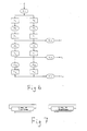
- Figure 6 shows the generation of the 16 sub-keys.
- the original key K of 64 bits is subjected to a fixed permutation PC-1 (permuted choice 1) with the aid of a table.
- PC-1 permuted choice 1
- the parity bits are extracted and the remaining 56 bits are changed over.
- the parity bits make up every 8th bit in the original 64-bit word.
- the 56 bits are further divided into two halves of 28 bits C o , Do.
- Sub-keys K, to K 16 will be formed and this is done with left-hand rotation of C and D as shows in Figure 7.
- the number of shifts, rotations which will be carried out is determined by a table. After K 16 has been shifted forward (28 shifts), the original value according to PC-1 is generated.
- the multiplexer in front of the registers has three different signals to select from: data in, the new data of the algorithm from function f, and the earlier data of the register.
- the MUX block becomes relatively extensive.
- a 56-bit key will thus be entered into a register and subjected to a number of shifts of different length before each instant in the encryption. According to the invention, this is achieved by means of a combinatorial block in order to avoid retarding the process with an extra control unit. With a network of 768 transmission gates and control logic, the right bit can be forwarded to the right output, which then replaces the LS block in Figure 6.
- S-boxes The largest proportion of the block is taken up by the so-called S-boxes. There are 8 storage units with six inputs and four outputs in each box. These are built up discretely with the aid of gates and function as fixed memories with given output data for each address.
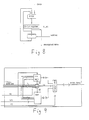
- Figure 9 shows how the encryption circuit appears to the computer system.
- the input signals are a 13- bit address bus, Chip Enable (CE), read/write (R/W) and output enable (OE).
- CE Chip Enable
- R/W read/write
- OE output enable
- the data is output and input on an 8-bit data. bus.
- the RAM block listens to all thirteen bits while the encryption block only uses five bits.
- a decoder (DEC) puts out the right CE signal to the right block on the basis of the address.
- OE controls the output buffer (three-state multiplexer) which is two-way for data writing.
- the encryption circuit looks like a memory circuit with 32 memory positions of 8 bits each, in other words one byte.
- the operations which can be carried out are: writing-in of data or key block, respectively, starting encryption or decryption, reading of status and reading of encrypted data.
- Data, encryption and key block are all of 64 bits each. Since the data bus of the circuit has 8 bits width, the block must be written and read in 8 part blocks.
- the data bus is used for the block and status but start and the choice of encryption/decryption are controlled by writing with certain address bits set to 1 or 0. The value of the data bus has no significance in this connection.
- the functions are determined by the address bits Ao to A4.
- a 2 -Ao represents the 8 addresses of the part-blocks in the data or key block.
- A3 has the function of register selection.
- the key can be written in but not read out.
- encrypted/decrypted data can be read out after the status has been read.
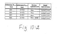
- FIG. 10 shows all possible read and write operations the circuit can be subjected to. As can be seen, there are many redundant registers in the memory map. Addresses of interest are those which have been marked in bold lettering. The functions in brackets are duplicates.
- the absolute addresses for the circuit are obtained by adding $1 FEO to the above addresses. A column with these is also given.
- the invention thus provides an encryption circuit with many advantages.
- the encryption circuit is integrated on one chip and has a pin configuration which corresponds to a standard memory.
- the encryption circuit can thus be directly placed in the existing equipment in place of a random access memory (RAM).
- the encryption bit itself only takes up 32 memory positions (bytes) of 8 kbytes (8192).
- the 32 bytes must be handled by the operating system in such a manner that they are not used as RAM positions.
- the RAM area itself is not used in any way by the encryption/decryption unit, but instead this may be eliminated if the rest of the system does not require the memory area.
- a single data register is used for implementing the 16 steps in the DES algorithm.
- the 64-bit register is implemented with the aid of the 32 memory positions of 1 byte each. A part of the memory positions is thus redundant.
- a suitable logic comprising, inter alia, a three-state multiplexer which selects one of three buses, a considerable simplification of the circuit is thus made possible.
- a third aspect of the invention is that the sub-keys in the DES algorithm are generated with the aid of combinational logic. This technique is very quick and does not result in any delay in the data rate.
Landscapes
- Engineering & Computer Science (AREA)
- Computer Security & Cryptography (AREA)
- Computer Networks & Wireless Communication (AREA)
- Signal Processing (AREA)
- Storage Device Security (AREA)
Applications Claiming Priority (2)
| Application Number | Priority Date | Filing Date | Title |
|---|---|---|---|
| SE8902165A SE464991B (sv) | 1989-06-16 | 1989-06-16 | Krypteringskrets uppbyggd med grindmatristeknik |
| SE8902165 | 1989-06-16 |
Publications (3)
| Publication Number | Publication Date |
|---|---|
| EP0403456A2 true EP0403456A2 (de) | 1990-12-19 |
| EP0403456A3 EP0403456A3 (de) | 1991-01-16 |
| EP0403456B1 EP0403456B1 (de) | 1995-10-04 |
Family
ID=20376293
Family Applications (1)
| Application Number | Title | Priority Date | Filing Date |
|---|---|---|---|
| EP19900850188 Expired - Lifetime EP0403456B1 (de) | 1989-06-16 | 1990-05-18 | Verschlüsselungsschaltung |
Country Status (3)
| Country | Link |
|---|---|
| EP (1) | EP0403456B1 (de) |
| DE (1) | DE69022780T2 (de) |
| SE (1) | SE464991B (de) |
Cited By (4)
| Publication number | Priority date | Publication date | Assignee | Title |
|---|---|---|---|---|
| GB2367461A (en) * | 2000-06-12 | 2002-04-03 | Hynix Semiconductor Inc | Encryption apparatus using Data Encryption Standard (DES) |
| GB2367462A (en) * | 2000-06-13 | 2002-04-03 | Hynix Semiconductor Inc | Key scheduler for Data Encryption Standard (DES) |
| CN1102310C (zh) * | 1994-07-14 | 2003-02-26 | 林仙坎 | 一种文件加密处理方法 |
| EP0903886A3 (de) * | 1997-09-18 | 2004-01-02 | Matsushita Electric Industrial Co., Ltd. | Übertragungsverfahren und -Vorrichtung zum kombinierten Multiplexen und Verschlüsseln |
Family Cites Families (3)
| Publication number | Priority date | Publication date | Assignee | Title |
|---|---|---|---|---|
| US4274085A (en) * | 1979-06-28 | 1981-06-16 | Motorola, Inc. | Flexible mode DES system |
| DE3631992A1 (de) * | 1986-03-05 | 1987-11-05 | Holger Sedlak | Kryptographie-verfahren und kryptographie-prozessor zur durchfuehrung des verfahrens |
| US4771462A (en) * | 1987-02-18 | 1988-09-13 | Hannan Forrest A | Communication port encryption/decryption method and apparatus |
-
1989
- 1989-06-16 SE SE8902165A patent/SE464991B/sv not_active IP Right Cessation
-
1990
- 1990-05-18 DE DE1990622780 patent/DE69022780T2/de not_active Expired - Fee Related
- 1990-05-18 EP EP19900850188 patent/EP0403456B1/de not_active Expired - Lifetime
Cited By (8)
| Publication number | Priority date | Publication date | Assignee | Title |
|---|---|---|---|---|
| CN1102310C (zh) * | 1994-07-14 | 2003-02-26 | 林仙坎 | 一种文件加密处理方法 |
| EP0903886A3 (de) * | 1997-09-18 | 2004-01-02 | Matsushita Electric Industrial Co., Ltd. | Übertragungsverfahren und -Vorrichtung zum kombinierten Multiplexen und Verschlüsseln |
| GB2367461A (en) * | 2000-06-12 | 2002-04-03 | Hynix Semiconductor Inc | Encryption apparatus using Data Encryption Standard (DES) |
| GB2367461B (en) * | 2000-06-12 | 2004-01-21 | Hynix Semiconductor Inc | Encryption apparatus using data encryption standard algorithm |
| US7099470B2 (en) | 2000-06-12 | 2006-08-29 | Hynix Semiconductor Inc. | Encryption apparatus using data encryption standard algorithm |
| GB2367462A (en) * | 2000-06-13 | 2002-04-03 | Hynix Semiconductor Inc | Key scheduler for Data Encryption Standard (DES) |
| GB2367462B (en) * | 2000-06-13 | 2004-04-14 | Hynix Semiconductor Inc | Key Schedular for encryption apparatus using data encryption standard algorithm |
| US7123720B2 (en) | 2000-06-13 | 2006-10-17 | Hynix Semiconductor, Inc. | Key scheduler for encryption apparatus using data encryption standard algorithm |
Also Published As
| Publication number | Publication date |
|---|---|
| SE8902165L (sv) | 1990-12-17 |
| SE464991B (sv) | 1991-07-08 |
| DE69022780D1 (de) | 1995-11-09 |
| DE69022780T2 (de) | 1996-03-14 |
| EP0403456B1 (de) | 1995-10-04 |
| EP0403456A3 (de) | 1991-01-16 |
| SE8902165D0 (sv) | 1989-06-16 |
Similar Documents
| Publication | Publication Date | Title |
|---|---|---|
| CA1318028C (en) | System and method for providing for secure encryptor key management | |
| US7092400B2 (en) | Method of transmitting data through a data bus | |
| EP0556928B1 (de) | Anordnung zum Verschlüsseln und Entschlüsseln von Daten, die auf eine Speicherplatte geschrieben oder von ihr gelesen werden mittels des DES-Algorithmus | |
| JP7107670B2 (ja) | ビットミキサにより暗号ラウンド鍵を生成するためのシステム及び方法 | |
| US7451288B2 (en) | Word-individual key generation | |
| US4797928A (en) | Encryption printed circuit board | |
| US4386234A (en) | Cryptographic communication and file security using terminals | |
| US4203166A (en) | Cryptographic file security for multiple domain networks | |
| US5224166A (en) | System for seamless processing of encrypted and non-encrypted data and instructions | |
| Sorkin | Lucifer, a cryptographic algorithm | |
| US5631960A (en) | Autotest of encryption algorithms in embedded secure encryption devices | |
| US5008935A (en) | Efficient method for encrypting superblocks of data | |
| US4238853A (en) | Cryptographic communication security for single domain networks | |
| US9602281B2 (en) | Parallelizable cipher construction | |
| KR100352783B1 (ko) | 소프트웨어/데이터 송수신 장치 | |
| GB2315575A (en) | Encryption circuit in I/O subsystem | |
| US5860094A (en) | System for protecting information stored on physical media | |
| US20240007283A1 (en) | Cryptographic device using transposition function and/or mapping function and cryptographic method thereof | |
| EP0403456B1 (de) | Verschlüsselungsschaltung | |
| JPH045298B2 (de) | ||
| US4488001A (en) | Intellectual properties protection device | |
| JP2000076144A (ja) | 論理回路、マイクロコンピュータ、および論理回路・記憶回路間の通信方法 | |
| TWI895618B (zh) | 密碼裝置及其密碼方法 | |
| JPH06195268A (ja) | Icメモリカード及びそのデータ保護方法及び装置 | |
| JPH02112082A (ja) | マイクロプロセッサおよびそれを用いたicカード |
Legal Events
| Date | Code | Title | Description |
|---|---|---|---|
| PUAI | Public reference made under article 153(3) epc to a published international application that has entered the european phase |
Free format text: ORIGINAL CODE: 0009012 |
|
| PUAL | Search report despatched |
Free format text: ORIGINAL CODE: 0009013 |
|
| AK | Designated contracting states |
Kind code of ref document: A2 Designated state(s): BE CH DE FR GB LI |
|
| AK | Designated contracting states |
Kind code of ref document: A3 Designated state(s): BE CH DE FR GB LI |
|
| RHK1 | Main classification (correction) |
Ipc: H04L 9/00 |
|
| 17P | Request for examination filed |
Effective date: 19910227 |
|
| 17Q | First examination report despatched |
Effective date: 19931213 |
|
| RAP1 | Party data changed (applicant data changed or rights of an application transferred) |
Owner name: TELIA AB |
|
| GRAA | (expected) grant |
Free format text: ORIGINAL CODE: 0009210 |
|
| AK | Designated contracting states |
Kind code of ref document: B1 Designated state(s): BE CH DE FR GB LI |
|
| REF | Corresponds to: |
Ref document number: 69022780 Country of ref document: DE Date of ref document: 19951109 |
|
| ET | Fr: translation filed | ||
| PLBE | No opposition filed within time limit |
Free format text: ORIGINAL CODE: 0009261 |
|
| STAA | Information on the status of an ep patent application or granted ep patent |
Free format text: STATUS: NO OPPOSITION FILED WITHIN TIME LIMIT |
|
| 26N | No opposition filed | ||
| PGFP | Annual fee paid to national office [announced via postgrant information from national office to epo] |
Ref country code: FR Payment date: 19990402 Year of fee payment: 10 |
|
| PGFP | Annual fee paid to national office [announced via postgrant information from national office to epo] |
Ref country code: DE Payment date: 19990420 Year of fee payment: 10 |
|
| PGFP | Annual fee paid to national office [announced via postgrant information from national office to epo] |
Ref country code: CH Payment date: 19990507 Year of fee payment: 10 |
|
| PGFP | Annual fee paid to national office [announced via postgrant information from national office to epo] |
Ref country code: BE Payment date: 19990526 Year of fee payment: 10 |
|
| PGFP | Annual fee paid to national office [announced via postgrant information from national office to epo] |
Ref country code: GB Payment date: 20000221 Year of fee payment: 11 |
|
| PG25 | Lapsed in a contracting state [announced via postgrant information from national office to epo] |
Ref country code: LI Free format text: LAPSE BECAUSE OF NON-PAYMENT OF DUE FEES Effective date: 20000531 Ref country code: CH Free format text: LAPSE BECAUSE OF NON-PAYMENT OF DUE FEES Effective date: 20000531 Ref country code: BE Free format text: LAPSE BECAUSE OF NON-PAYMENT OF DUE FEES Effective date: 20000531 |
|
| BERE | Be: lapsed |
Owner name: TELIA A.B. Effective date: 20000531 |
|
| REG | Reference to a national code |
Ref country code: CH Ref legal event code: PL |
|
| PG25 | Lapsed in a contracting state [announced via postgrant information from national office to epo] |
Ref country code: FR Free format text: LAPSE BECAUSE OF NON-PAYMENT OF DUE FEES Effective date: 20010131 |
|
| PG25 | Lapsed in a contracting state [announced via postgrant information from national office to epo] |
Ref country code: DE Free format text: LAPSE BECAUSE OF NON-PAYMENT OF DUE FEES Effective date: 20010301 |
|
| REG | Reference to a national code |
Ref country code: FR Ref legal event code: ST |
|
| PG25 | Lapsed in a contracting state [announced via postgrant information from national office to epo] |
Ref country code: GB Free format text: LAPSE BECAUSE OF NON-PAYMENT OF DUE FEES Effective date: 20010518 |
|
| GBPC | Gb: european patent ceased through non-payment of renewal fee |
Effective date: 20010518 |