EP0403396A1 - Device for monitoring the operation of a microcontroller or microprocessor - Google Patents
Device for monitoring the operation of a microcontroller or microprocessor Download PDFInfo
- Publication number
- EP0403396A1 EP0403396A1 EP90401689A EP90401689A EP0403396A1 EP 0403396 A1 EP0403396 A1 EP 0403396A1 EP 90401689 A EP90401689 A EP 90401689A EP 90401689 A EP90401689 A EP 90401689A EP 0403396 A1 EP0403396 A1 EP 0403396A1
- Authority
- EP
- European Patent Office
- Prior art keywords
- input
- output
- monitoring device
- flip
- reset
- Prior art date
- Legal status (The legal status is an assumption and is not a legal conclusion. Google has not performed a legal analysis and makes no representation as to the accuracy of the status listed.)
- Granted
Links
Images


Classifications
-
- G—PHYSICS
- G06—COMPUTING; CALCULATING OR COUNTING
- G06F—ELECTRIC DIGITAL DATA PROCESSING
- G06F11/00—Error detection; Error correction; Monitoring
- G06F11/07—Responding to the occurrence of a fault, e.g. fault tolerance
- G06F11/0703—Error or fault processing not based on redundancy, i.e. by taking additional measures to deal with the error or fault not making use of redundancy in operation, in hardware, or in data representation
- G06F11/0751—Error or fault detection not based on redundancy
- G06F11/0754—Error or fault detection not based on redundancy by exceeding limits
- G06F11/0757—Error or fault detection not based on redundancy by exceeding limits by exceeding a time limit, i.e. time-out, e.g. watchdogs
-
- G—PHYSICS
- G06—COMPUTING; CALCULATING OR COUNTING
- G06F—ELECTRIC DIGITAL DATA PROCESSING
- G06F1/00—Details not covered by groups G06F3/00 - G06F13/00 and G06F21/00
- G06F1/24—Resetting means
Definitions
- the present invention relates to a device for monitoring the operation of a microcontroller or microprocessor, in particular but not exclusively for application to motor vehicles.
- microcontrollers and microprocessors generally deliver on one of their outputs, a control signal whose frequency depends on the operation of the microcontroller or microprocessor, that is to say the progress of programming.
- Such monitoring is particularly useful when microcontrollers or microprocessors are used in environments highly disturbed by electromagnetic interference, as is the case in particular in motor vehicles.
- the circuits proposed for this purpose are generally formed by two monostables which have corresponding switching times respectively to the minimum period and to the maximum period admissible in normal operation of the control signal generated by the microprocessor.
- the present invention now aims to provide a new monitoring device which eliminates the drawbacks of prior devices.
- An auxiliary object of the present invention is to provide a circuit that can be integrated into a single housing.
- Another auxiliary object of the present invention is to provide a more precise device than the devices prior to two monostable devices.
- Another auxiliary object of the present invention is to provide a monitoring device allowing easy and fairly wide adjustment of the authorized frequency range.
- a monitoring device comprising: - an oscillator which delivers a timing signal of constant and known frequency, a programmable frequency divider which returns the clock signal as input and delivers a clock signal at its output, the period of which is linked to the minimum period to be checked, - a counter receiving the clock signal, which generates time windows, and - an event controller which controls the state of the control signal generated by a microprocessor or microcontroller during said time windows.
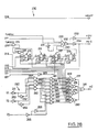
- FIG. 1 appended Found in FIG. 1 appended are the four main functional blocks of the monitoring device according to the present invention, previously indicated: an oscillator 100, a frequency divider 200, a counter 300 and an event controller 400.
- the function of the oscillator 100 is to deliver a timing signal of constant and known frequency.
- the frequency divider 200 is programmable. It receives as input the timing signal generated by the oscillator 100 and delivers at its output 201 a clock signal HC whose period is linked to the minimum period authorized for the control signal from the microcontroller or microprocessor.
- the counter 300 receives the clock signal HC and generates time windows therefrom. These time windows are identified by the validation of flags on the outputs TM, DBFl and FINF of the counter, that is to say a passage to the high level of these outputs.
- the event controller 400 receives the control signal from the microcontroller or microprocessor and monitors the state of this control signal during the time windows generated by the counter 300.
- the control signal generated by the microcontroller or microprocessor is referenced SM in the attached figures.
- the event controller 400 In the event of an anomaly observed, that is to say when the period of the control signal SM leaves a defined range, the event controller 400 generates a reset signal from the microcontroller or microprocessor on its RESET output. .
- the oscillator module 100 in fact comprises two oscillators 110, 120, associated with respective crystals 112, 122, and connected respectively to the input terminals OSLOW and OSQUIC of the frequency divider 200.
- These oscillators 110, 120 can work for example in the frequency range from 2 to 20 MHz for the oscillator 110 and in the range from 20 to 32 MHz for the oscillator 120. Only one of the two oscillators 110, 120 is set service to control the monitoring circuit. The choice of the oscillator to activate depends on the frequency of the control signal generated by the microcontroller or microprocessor to be monitored.
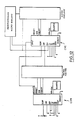
- FIGS. 2A and 2B The diagram of the frequency divider 200 is shown in FIGS. 2A and 2B which are complementary.
- the frequency divider 200 comprises on the one hand a set 210 of flip-flops connected in cascade to divide the frequency of the timing signal OSLOW or OSQUIC coming from the oscillator 100, on the other hand a multiplexer 250 which generates the clock signal HC from signals generated by the flip-flop set 210, as a function of an external three-bit programming word applied to inputs V1, V2, V3 of the module.
- two sets of four flip-flops 211, 212, 213, 214 are provided on the one hand, and 215, 216, 217 and 218 on the other hand.
- the OSLOW and OSQUIC inputs of module 200 are connected to the inputs of a NOR gate 219.
- the output of gate 219 attacks, via an inverter 220, the CLK clock inputs of flip-flops 211 and 215.
- the CLR reset inputs of flip-flops 211 to 218 receive, via inverters 221, 222, 223, a reset signal when the system is powered up, applied from outside the circuit to an input RAZlNIT.
- the output Q / of the flip-flop 211 is looped back to its input D and connected to the clock input CLK of the flip-flop 212 downstream. It is the same for the flip-flop 212 which has its output Q / looped back to its input D is connected to the clock input CLK of the flip-flop 213; the latter itself has its output Q / looped back to its input D and connected to the clock input CLK of the flip-flop 214.
- This flip-flop 214 has its output Q / looped back to its output D.
- the outputs Q of flip-flops 211, 212, 213 and 214 are connected to the respective inputs of a NAND gate 224. The output of this latter is connected to the input of a NAND gate 225. The second input of the NAND gate 225 receives a test signal applied from the outside to a TURBOH input.
- the output of the NAND gate 225 is connected to a first input of a door or exclusive 226.
- the second input of this door is connected to the output Q of the flip-flop 215.
- the output of the door or exclusive 226 attacks the input D of rocker 215.
- the Q / output of the flip-flop 215 is connected to the CLK clock input of the flip-flop 216.
- the Q / output of the flip-flop 216 is looped back to its D input and is connected to the CLK clock input of the flip-flop 217.
- the output Q / of the bacule 217 is looped back to its input D and connected to the clock input CLK of the flip-flop 218.
- the output Q / of flip-flop 218 is looped back to its input D.
- the frequency of the oscillator 110 or 120 used to drive the monitoring circuit is available on an HBUFF output of the module 200. In fact, this output is connected to the output of the NOR 219 door by means of two non- series 227, 228.
- the divider module 200 delivers on outputs HDIV and PHI1 a signal whose frequency corresponds to that of the oscillator 110 or 120 used, divided by 256.
- the signals HDIV and PHI1 are obtained on the basis of the outputs Q of the flip-flops 211, 218 and a TURPHI test signal.
- the TURPHI test input of the module 200 as well as the Q output of the flip-flop 211 are connected to the inputs of an ET229 gate.
- a second gate ET230 receives on its inputs the output Q of the flip-flop 218, and the signal TURPHI supplemented by a gate NO 231.
- the outputs of the gates E229, 230 attack the inputs of a gate NOR 232.
- the output of the gate NOR 232 is connected to the HDIV and PHI1 outputs of module 200 respectively by NON gates 233, 234.
- the HDIV output can be used to drive a microcontroller.
- the PHI1 output is used to control the event controller 400.
- the purpose of the mutiplexer 250 is to generate the clock signal HC on the basis of the intermediate frequency signals generated by the set of flip-flops 210, and on the basis of the programming word defined on the inputs V1, V2, V3 .
- the multiplexer 250 is formed of NON gates 251, 252, 253, 254, 255, 256, NAND gates with two inputs 257, 258, 259, 260, NOR gates 261, 262, 263, 264, 265, 266, 267 and 268, AND doors with two inputs 269, 270, 271, 272, 273, 274, 275, 276, NOR doors 277, 278, 279, 280 and one NAND gate with four inputs 281.
- the gates 251 to 268 define a logical combination of the inputs V1, V2 and V3.
- the outputs of gates 261 to 268 are connected to one of the inputs of AND gates 269 to 276.
- the second input of these gates 269 to 276 receives one of the outputs Q of flip-flops 211 to 217 or the output of gate 234
- the multiplexer 250 with logic gates in FIG. 2B can be the subject of various variant embodiments. For this reason, the particular structure of the multiplexer, that is to say the exact connections defined between the logic gates, will not be described in more detail below.
- the logic state imposed on the inputs V1, V2 and V3, which corresponds to the programming word of the division, makes it possible to indirectly define the minimum period threshold for the control signal from the microcontroller or the microprocessor.
- the state of the inputs V1, V2 and V3 makes it possible to determine the frequency of the clock signal HC, and the minimum period threshold is defined by the counter 300 as being equal to a multiple of the period of the clock signal HC.
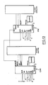
- the structure of the counter 300 is shown in Figures 3A, 3B, taken in combination.
- the essential function of the counter 300 is to generate, from the clock signal HC, time windows.
- the essential function of the counter 300 is to generate three flags: a first flag defining a so-called dead time period during which the state of the control signal generated by the microcontroller to the microprocessor is indifferent, and two flags corresponding respectively to the minimum period and the maximum period between which the period of the control signal must lie.
- the counter 300 is essentially made up of fifteen flip-flops 301 to 315 connected in cascade, clocked by the clock signal HC, and associated with flip-flops making it possible to store the flags of dead time and minimum period generated by flip-flops 301 at 315.
- the clock signal HC from the frequency divider 200 is applied to the clock inputs CLK of the flip-flop 301, of the flip-flop 304 and of the flip-flop 308, by means of an inverter 316.
- the CLR reset inputs of flip-flops 301 to 315 receive an internal reset reset signal generated by the event controller 400 according to methods which will be described later.
- the reset signal is applied to the flip-flops 301 to 315 via inverters 317 to 321.
- the Q / output of flip-flop 301 is looped back to its D input and connected to the CLK clock input of the downstream flip-flop 302.
- the Q / output of flip-flop 302 is looped back to its D input and connected to the input CLK clock of flip-flop 303.
- the Q / output of flip-flop 303 is connected to its input D.
- the Q outputs of flip-flops 301, 302 and 303 are connected to the inputs of a NAND gate 322.
- the output of gate 322 is connected to a first input of a NAND gate 323 whose second input receives via an inverter 324 a TURBOC test signal applied from the outside.
- the output of door 323 is connected to a first input of a door or exclusive 325, the second input of which receives the output Q of the flip-flop 304.
- the gate output or exclusive 325 is connected to the input D of the flip-flop 304.
- the Q / output of flip-flop 304 is connected to the input d CLK clock of flip-flop 305.
- the output Q / of flip-flop 305 is looped back to its input D and connected to the CLK input of flip-flop 306.
- the output Q / of flip-flop 306 is looped back to its input D and connected at the CLK clock input of flip-flop 307.
- the Q / output of flip-flop 307 is looped back to its input D.
- the output of the NAND gate 322 and the Q output of the flip-flop 304 attack the inputs of a NOR gate 326.
- the inputs of a NAND gate 327 receive the output of this gate 326 as well as the Q outputs of the flip-flops 305 to 307.
- the same output of the NAND gate 328 is connected to one of the inputs of a gate or exclusive 329 which receives on its second input the output Q of the flip-flop 308.
- the output of the door or exclusive 329 is connected to the input D of the flip-flop 308.
- the output Q / of the flip-flop 308 is connected to the clock input CLK of the flip-flop 309.
- the Q / output of the flip-flop 309 is looped back to its D input and connected to the CLK clock input of flip-flop 310.
- the Q / output of flip-flop 310 is looped back to its D input and connected to the CLK clock input of flip-flop 311
- the Q / output of flip-flop 311 is looped back to its D input and connected to the CLK clock input of flip-flop 312.
- the Q / output of flip-flop 312 is looped back to its D input and connected to the input CLK clock of flip-flop 313.
- the Q / output of flip-flop 313 is looped back to its D input and connected to the CLK clock input of flip-flop 314.
- the Q / output of flip-flop 314 is looped back to its input D and connected to the CLK clock input of flip-flop 315.
- the Q / output of flip-flop 315 is looped back to its input D.
- the dead time, minimum period and maximum period flags are available respectively on outputs referenced TN, DBF1 and FINF of the counter 300.
- the dead time flag available on the output TM is defined using the output Q of the flip-flop 310 memorized on a flip-flop SR formed by two NOR gates 330, 331. For this the output Q of the flip-flop 310 is applied to a first input of door 330. The output of door 330 is connected to a first input of door 331. The latter receives on its second input the reset internal reset signal via the inverter 317 The output of door 331 is connected to the output TM of the counter 300. It is also looped back to the second input of door 330.
- the flag corresponding to the minimum period, available on the output DBF1 is defined on the basis of the output Q of the flip-flop 313, stored on a flip-flop SR formed by two NOR gates 332, 333.
- the output Q of flip-flop 313 is connected to a first input of door 332.
- the output of door 332 is connected to a first input of door 333. This receives on its second input the internal reset signal by l intermediary of the inverter 317.
- the output of the NOR gate 303 is connected to the output DBF1 of the counter 300. It is moreover connected to the second input of the gate 332.
- the duration of the dead time defined by the flag TM corresponds to 1/8 of the minimum period defined by the flag DBF1.
- the maximum period flag, available on the FINF output of the counter 300 is defined as desired on the basis of the Q output of the flip-flop 314, or on the basis of the Q output of the flip-flop 315.
- the choice between these two possibilities is made by checking the state of a TL input of the circuit.
- the output Q of the flip-flop 314 is connected to a first input of an AND gate 334, which receives on its second input, via an inverter 335, the control signal TL.
- the output Q of the flip-flop 315 is in turn connected to the first input of an AND gate 336 which receives on its second input the signal TL.
- the outputs of doors 334, 336 are connected to the inputs of a NOR gate 337, the output of which is connected to the terminal FINF via an inverter 338.
- the maximum period controlled, defined by the FINF flag corresponds either to twice the minimum period defined by the DBF1 flag, or to four times this minimum period.
- flip-flops 301 to 315 are mounted as asynchronous counters, a re-synchronization on the basis of the clock signal HC being provided at the input of flip-flops 301, 304 and 308.
- the TURBOC test signal makes it possible to inhibit the part of the counter formed by the flip-flops 301 to 307, to operate in test mode at a faster frequency. However, in normal mode of monitoring the operation of the microcontroller or microprocessor, the TURBOC test signal is inhibited.
- the structure of the event controller 400 is shown in FIGS. 4A and 4B complementary.
- the main function of the event controller 400 is to control the state of the control signal generated by the microcontroller or microprocessor, during the time windows defined by the counter 300.
- the control signal generated by the microcontroller or microprocessor is applied to the input SM of the event controller 400.
- the purpose of the event controller 400 is to verify that the control signal SM passes indeed from the low level to the high level between the minimum period defined by the flag DBF1 and the maximum period defined by the flag FINF.
- the event controller ensures a reset of the counter 300, and therefore of the time windows, by validation of the reset signal.
- the event controller generates a reset signal from the microcontroller or microprocessor, on its RESET output when one of the following conditions is detected: - the control signal SM is not at the logic zero level at the end of the dead time defined by the flag TM, - the SM signal goes from low logic level to high logic level before validation of the DBF1 flag of minimum period, or - the control signal SM does not pass from the low logic level to the high logic level before the validation of the FINF flag corresponding to the maximum admissible period.
- the state of the control signal SM generated by the microcontroller or microprocessor is ignored as long as the dead time flag TM is not validated, that is to say as long as this flag TM is at zero.
- control signal SM is applied to a first input of a NOR 401 gate, the output of which is connected to the first input of a NOR 402 gate.
- the output of the NOR 402 gate is looped back to the second input of the door 401.
- the second input of the door 402 receives the signal TM via an inverter 403.
- the signal coming from the gate 402, as well as the flags DBF1 and FINF are the object of a double memorization, in flip-flops 404 to 409, successively on the rising edge then on the falling edge of the signal PHI1 coming from the frequency divider 200.
- the output of the gate 402 is connected to the input D of the flip-flop 404.
- the output Q of this flip-flop 404 is connected to the input D of the flip-flop 405.
- the flag DBF1 of minimum period is applied to the input D of the flip-flop 406.
- the output Q of this flip-flop 406 is connected to input D of flip-flop 407.
- the maximum period flag defined on the FINF input is applied to the D input of the flip-flop 408.
- the Q output of this is applied to the D input of the flip-flop 409.
- the CLK clock inputs of the flip-flops 404, 406 and 408 receive the PHI1 signal via two inverters 410, 411.
- the CLK clock inputs of the output flip-flops 405, 407 and 409 receive the PHI1 signal complemented by three inverters 410, 412 and 413.
- the CLR reset inputs of the output flip-flops 405, 407 and 409 receive the reset signal on power-up RAZINIT, applied from the outside, via inverters 414, 415.
- the inputs of resetting the input flip-flops 404, 406 and 408 receive an internal reset signal, corresponding to the RESET signal, defined at the output of an inverter 416 according to methods which will be defined later.
- the event controller 400 comprises a logic module formed by three NOR doors 417, 418, 419 and two NAND doors 420, 421 which combine the outputs of flip-flops 405, 407 and 409, to verify that the SM control signal available to the exit from gate 402 when the dead time flag TM is at the high logic level, itself passes from the low logic level to the high logic level between the validation of the two flags DBF1 and FINF.
- the NOR gate 417 receives on its inputs the outputs Q / of the gates 405 and 407.
- the NOR gate 418 receives on its inputs the output Q / of the flip-flop 405 and the output Q of flip-flop 407.
- NOR gate 419 receives on its inputs the output of gate 418 and the Q output of flip-flop 409.
- gate NOR 417 The output of gate NOR 417 is validated when the control signal SM passes from the low logic level to the high logic level after validation of the flag DBF1. This information is stored on a flip-flop 422 which receives on its input D the output of door 417. The output Q / of the flip-flop 422 is used to generate the internal reset signal RESET, that is to say to reset the counter 300 and the corresponding time windows.
- the output of the NOR gate 419 is connected to a first input of a NAND gate 420 which receives on its second input a signal derived from the control signal MV, according to methods which will be explained later.
- the output of gate 420 is validated in the event of detection of abnormal operation, that is to say when the signal SM is at zero at the end of the dead time defined by the flag TM, or even when the signal SM goes to high logic level before validation of the flag DBF1, or even when the control signal SM does not pass to the high logic level before the validation of the flag of maximum period FINF.
- the information available on the output of door 420 is stored in a flip-flop 423 whose input D is connected to the output of door 420.
- the Q / output of flip-flop 423 is used to generate the RESET signal for general reset from the microprocessor to the microcontroller.
- CLK clock inputs of flip-flops 422, 423 receive signal PHI1 via inverters 410, 411.
- CLR reset inputs of flip-flops 422, 423 receive signal RAZINIT of reset to power-up via inverters 414 and 415.
- a NAND gate 425 receives respectively on its three inputs the output Q / of the flip-flop 422, the signal RAZINIT of general reset at power-up, by means of an inverter 424, and the output of a NAND gate 421. This receives on its inputs respectively the output of gate NOR 419 and the output of gate NAND 425.
- the output of this door 425 is connected to a DFLT output terminal of the device via an inverter 426.
- the DFLT output goes to 1 when the period of the control signal generated by the microcontroller to the microprocessor leaves the authorized window . In in other words, the DFLT output goes to 1 in the event of a malfunction of the microcontroller or microprocessor.
- a NAND gate with two inputs 428 receives on its inputs the output Q / of the flip-flop 423 and an external signal SDR.
- the output of gate 428 is connected via two inverters 429, 430 to the RESET output terminal of the monitoring device, on which the reset signal of the microcontroller or microprocessor is available.
- RESETB the terminal referenced RESETB
- a NAND gate 427 with four inputs receives a signal derived from the control signal MV, the output Q / of the flip-flop 422 and the output of the inverter 429 and the output of the inverter 424.
- the output of gate 427 is connected at the input of the inverter 416. It is also connected to the reset output via an inverter 402.
- the reset signal of the counter 300 in the event of detection of correct operation, is available on the reset terminal.
- the same signal, complemented, is available on the output referenced SYNCRAZ, which is connected to the output of the inverter 432 via an inverter 433.
- the DR and MV signals are processed by a set of ten flip-flops 434 to 443.
- the signal DR is applied to the input D of the flip-flop 434.
- the output Q of this flip-flop is connected to the input D to the flip-flop 439.
- the Q output of the flip-flop 439 is connected to the input D of the flip-flop 438.
- the output Q of the flip-flop 438 is connected to the input D of the flip-flop 443.
- the signal MV is applied to the input D of the flip-flop 435.
- the output Q of the flip-flop 435 is connected to the input D of the flip-flop 440.
- the output Q of the flip-flop 440 is connected to the input D of the flip-flop 436.
- the output Q of flip-flop 436 is connected to the input D of flip-flop 441.
- the output Q of flip-flop 441 is connected to input D of flip-flop 437.
- the Q output of flip-flop 437 is connected to the D input of flip-flop 442.
- the CLR reset inputs of flip-flops 434 to 443 receive the RAZINIT signal via inverters 444, 445.
- the CLK clock inputs of flip-flops 434 to 438 receive the PHI1 signal through inverters 410 , 446.
- the flip-flops 439 to 443 receive the signal PHI1 complemented via three inverters 410, 412 and 447.
- the Q output of flip-flop 439 and the Q / output of flip-flops 442 and 443 are combined in a NAND gate 448 The output of the latter attacks the input of the NAND gate 420. Furthermore the output Q of the flip-flop 436 attacks one of the inputs of the NAND gate 427.
- the monitoring system also includes: - the HBUFF output which gives a square signal with a frequency equal to that of the quartz used as an input, this output can be used to drive the input of the oscillator cell of the microcontroller, - an HDIV output which delivers a signal with a frequency equal to that of the quartz used divided by 256, - a PRC test output, - a DBF output indicating the start of the window authorized for the period of the control signal, by switching to the high state of this output, - a RESET output where high active RESET pulses are delivered, - a RESETB output where low active RESET pulses are delivered, - a DFLT output which goes to 1 if the period of the control signal generated by the microcontroller leaves the authorized window and a SYNCRAZ output indicating that the circuit carries out a reset to zero of these counters.
- the MV input enables validation or invalidation of the monitoring of the control signal generated by microcontrollers. If the MV input is set to zero, only the SDR and DR inputs are used to generate RESETs.
- SDR When the MV input is zero, SDR is the input triggering a priority RESET. This input can be used to generate a RESET pulse on power up. SDR is an active signal in a low state. The RESET pulse at power-up can therefore be generated using a circuit comprising a resistor and a capacitance in series between ground and a positive supply terminal, the SDR signal being taken at midpoint. of this series branch.
- the DR input makes it possible to trigger RESET pulses on each DR passage from the low state to the high state.
- the generation of the RESET pulse is only guaranteed if the width of the pulse present on DR is greater than the width of the RESET pulse.
- the RESET output of the circuit is active as long as the SDR input is at zero.
- the ascent of SDR triggers the microcontroller pulse monitoring sequence.
- the DR input When the MV signal rises, the DR input remains active for a time equal to the width of a RESET pulse. Then the states of the DR input are ignored.
- the pulse monitoring is activated.
- the monitoring sequence is initialized on the rising edge of MV.
- the DR input triggers a RESET
- the monitoring sequence is reinitialized on the falling edge of the RESET.
- the monitoring sequence of the control signal generated by a microcontroller begins with a reinitialization of the counter 300 and of the corresponding time windows. Then, the counters are released, and the time windows represented by the flags TM, DBF1 (TMIN) and FINF (TMAX) are generated.
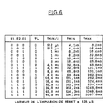
- FIG. 5 There is shown diagrammatically in FIG. 5 a chronogram of the flags TM, TBF1 and FNIF.
- the window defined by the flag DBF1 equals eight times the window defined by the flag TM, while the flag defined by FINF equals twice the flag defined by DBF1.
- the microcontroller has a TMIN / 8 time called dead time, during which the states which it sends on the SM input are ignored. If at the end of this delay the SM input is not at zero, a RESET signal is generated. A re-initialization of the process is then restarted at the falling edge of the RESET.
- the microcontroller must maintain the SM input at zero between the validation of the TM flag and the validation of the DBF1 flag. If the entry SM however goes to one during this time window, a RESET pulse is generated and the reinitialization of the process is started.
- the microcontroller must deposit a pulse between the validation of the DBF1 flag and the validation of the FINF flag. If this is the case, the process of generation of the time windows by the counter 300 is re-initialized by validation of the reset signal at the moment when the pulse appears on SM. The function being considered as correct there is no generation of RESET pulse.
- the opening of the authorized period window is signaled at the output of the monitoring device by switching to one of the DBF output. When a reinitialization is carried out this output returns to zero.
- a RESET triggered by an oversized control signal on the SM input has the effect of switching the DFLT output to one. This output only goes back to zero if the microcontroller picks up a correct pulse generation. On power up the DFLT signal is initialized to zero.
- the windows defined by the flags TM, DBF1 and FINF are functions of the frequency of the quartz used as input and of the inputs V1, V2, V3 and TL.
- the dead time window defined by the flag TM has a duration equal to TMIN / 8, TMIN being the lower limit of the authorized period, defined by the flag DBF1.
- the upper limit of the authorized period is equal to 2TMIN if the TL input is zero and 4TMIN if the TL input is one.
- the width of the RESET pulse is equal to the period defined by the quartz divided by 256.
- the application shown in FIG. 7 appended corresponds to monitoring the operation of a microcontroller in asynchronous mode.
- the inputs DR, TL, V3 and TEST of the CV device are placed at the low logic level while the inputs MV, V1 and V2 of the CV device are placed at the high logic level.
- the SDR input is connected to the midpoint of a bridge comprising a resistor R and a capacitor C in series between the ground and the positive supply terminal, the capacitor being placed on the ground side.
- a crystal is connected to the OSLOW input of the circuit while the OSQUIC input is grounded.
- the circuit CV receives on its input SM the control signal generated by the microcontroller.
- the latter is controlled by the timing signal generated by the quartz, the HBUFF output of the CV device being connected to the microcontroller. Finally, if necessary, it is re-initialized thanks to the RESET signals generated by the CV circuit.
- the application represented in FIG. 8 corresponds to monitoring the operation of a microcontroller in synchronous mode, with monitoring of the operation of the monitoring device by the microcontroller.
- the application represented in FIG. 8 differs from that represented in FIG. 7 only by the fact that the input TL is placed at the high logic level and not at the low logic level on the one hand, and on the other hand and especially that the outputs DBF1 and SYNCRAZ of the CV monitoring device are connected to the microcontroller to indicate to it, by the DBF output, the validation of the flag of the minimum period, therefore the moment from which the microcontroller is authorized to place a pulse of the control signal, and indicate by the SYNCRAZ output that the CV monitoring device performs a reset zero of its counter 300 and therefore of the corresponding time windows.
- the application represented in FIG. 9 corresponds to monitoring the operation of a microcontroller with inhibition of the output interfaces thereof, from a fault detected in the operation of the microcontroller, until the return to normal operation of it.
- Figure 9 shows a CV monitoring device, a microcontroller and an output interface connected to the microcontroller.
- the application represented in FIG. 9 differs from that represented in FIG. 7 by the fact that on the one hand the input TL is at the high logic level and not at the low logic level and that on the other hand and above all the DFLT output of the CV monitoring device is connected to the inhibit input of the interface.
- the output DFLT of the circuit CV being at one as long as the period of the control signal leaves the authorized window, the output interface is inhibited as long as the operation of the microcontroller is abnormal.
- the application shown in Figure 10 corresponds to a periodic reset mode of the microcontroller.
- the input SM of the monitoring device CV does not receive the control signal from the microcontroller, but is placed at the low logic level.
- the counter 300 periodically abuts the maximum authorized period and validates the corresponding FINF flag. RESET pulses are thus generated periodically.
- the inputs and outputs of the CV monitoring device remain in accordance with the provisions described above with reference to FIG. 7, except that the input TL is again at the high logic level.
- the application represented in FIG. 11 corresponds to monitoring the operation of a microcontroller with the possibility of waking up a sleeping microcontroller by an external intervention, for example pressing a button or activating an infrared remote control receiver.
- FIG. 11 There is shown in Figure 11 attached a CV monitoring device receiving a quartz on its OSLOW input, a microcontroller, peripherals associated with motors, a key pressed detector, an infrared remote control receiver and a regulator.
- the regulator attacks the SDR input of the CV device.
- the TR input receives a logical combination of the output of external elements capable of waking up the microcontroller, for example an infrared remote control receiver or a key detector pressed as indicated previously, so that a wake-up pulse is applied to the DR circuit CV input when one of these elements is activated.
- the MV input of the CV monitoring device is connected to an output of the peripherals making it possible to indicate to the CV circuit whether or not the peripherals are energized.
- the TL, V1 and V2 inputs are at the high level.
- the V3 and TEST inputs are at the low level.
- the circuit CV receives on its input SM the control signal generated by the microcontroller.
- the RESET, HBUFF and HDIV outputs of the CV circuit are connected to the associated inputs of the microcontroller.
- the DFLT output of the CV monitoring device is connected to the inhibition input of the microcontroller's output devices.
- the application represented in FIG. 12 corresponds to an application using a master microcontroller and a slave microcontroller with the possibility for the master microcontroller to fall asleep and wake up the functions of the slave microcontroller.
- FIG. 12 schematically shows a master microcontroller associated with a first CVM monitoring device, and a slave microcontroller associated with a second CVE monitoring device.
- FIG. 12 also schematically depicts peripherals of the slave microcontroller.
- the SDR, DR, NY, TL, V1, V2, V3, TEST, OSLOW and OSQUIC inputs of the CVM device are connected as indicated above with reference to FIG. 8.
- the CVM circuit receives on its SM input the control signal from the microcontroller master. These RESET and HBUFF outputs are connected to the associated inputs of the master microcontroller. Its RESETB output is connected to the SDR input of the CVE circuit.
- the inputs DR and MV of the circuit CVE are connected to an associated terminal of the master microcontroller and to an authorization terminal of the peripherals of the slave microcontroller.
- the TL, V1 and V2 inputs of the CVE circuit are at the high logic level, the V3, TEST and OSQUIC inputs are at the low level.
- a crystal attacks the OSLOW input.
- the CVE circuit receives on its SM input the control signal generated by the slave microcontroller. These RESET and HBUFF outputs are connected to the associated inputs of the slave microcontroller. Finally, the DFLT output of the CVE circuit attacks an associated terminal of the master microcontroller as well as the inhibition input of the peripherals.
- FIG. 13 shows a master microcontroller associated with a first CVM monitoring circuit, as well as a slave microcontroller associated with a second CVE monitoring circuit.
- FIG. 13 is essentially distinguished from FIG. 12 by the absence of peripherals associated with the slave microcontroller. It follows that the output DFLT of the second monitoring device CVE is connected only to the master microcontroller and that the input DR of the device CVE is at low logic level while the input NV of the same circuit CVE is at high logic level.
Abstract
Description
La présente invention concerne un dispositif de surveillance du fonctionnement d'un microcontrôleur ou microprocesseur, en particulier mais non exclusivement pour application aux véhicules automobiles.The present invention relates to a device for monitoring the operation of a microcontroller or microprocessor, in particular but not exclusively for application to motor vehicles.
On sait que les microcontrôleurs et microprocesseurs délivrent généralement sur l'une de leur sortie, un signal de contrôle dont la fréquence dépend du fonctionnement du microcontrôleur ou microprocesseur, c'est-à-dire du déroulement de la programmation.It is known that microcontrollers and microprocessors generally deliver on one of their outputs, a control signal whose frequency depends on the operation of the microcontroller or microprocessor, that is to say the progress of programming.
On a déjà proposé de nombreux dispositifs de surveillance du fonctionnement d'un microcontrôleur ou microprocesseur, sensibles à ce signal de contrôle. Ces dispositifs sont dénommés généralement "chien de garde". La fonction essentielle de ces dispositifs de surveillance est de détecter toute anomalie éventuelle par surveillance de la fréquence du signal de contrôle et réinitialiser le microprocesseur ou microcontrôleur si nécessaire.Numerous devices have already been proposed for monitoring the operation of a microcontroller or microprocessor, sensitive to this control signal. These devices are generally called "watchdog". The essential function of these monitoring devices is to detect any possible anomaly by monitoring the frequency of the control signal and to reset the microprocessor or microcontroller if necessary.
Une telle surveillance est particulièrement utile lorsque les microcontrôleurs ou microprocesseurs sont utilisés dans des environnements fortement perturbés par des parasites électromagnétiques, comme cela est le cas notamment dans les véhicules automobiles.Such monitoring is particularly useful when microcontrollers or microprocessors are used in environments highly disturbed by electromagnetic interference, as is the case in particular in motor vehicles.
On a proposé tout d'abord, comme décrit par exemple dans les documents DE-A-2903638, DE-A-3214006 et DE-A-3035896, des circuits permettant de vérifier que la fréquence du signal de contrôle ne tombe pas sous un seuil représentatif d'un fonctionnement normal limite. L'efficacité de ces dispositifs de surveillance, qui se contentent de comparer la fréquence du signal de contrôle à un seuil, laisse cependant à désirer.First of all, as described for example in documents DE-A-2903638, DE-A-3214006 and DE-A-3035896, circuits have been proposed making it possible to verify that the frequency of the control signal does not fall below a threshold representative of normal limit operation. The effectiveness of these monitoring devices, which simply compare the frequency of the control signal to a threshold, leaves much to be desired.
On a également proposé pour surveiller le fonctionnement d'un microcontrôleur ou microprocesseur, comme décrit dans les documents JP-A-57108938, JP-A-57 108939 et DE-A-3240704, des circuits plus performants conçus pour vérifier que la fréquence du signal de contrôle tombe dans une plage définie de fonctionnement normal.It has also been proposed to monitor the operation of a microcontroller or microprocessor, as described in documents JP-A-57108938, JP-A-57 108939 and DE-A-3240704, more efficient circuits designed to verify that the frequency of the control signal falls within a defined range of normal operation.
Les circuits proposés à cet effet sont en général formés de deux monostables qui présentent des temps de basculement correspondant respectivement à la période minimale et à la période maximale admissibles en fonctionnement normal du signal de contrôle généré par le microprocesseur.The circuits proposed for this purpose are generally formed by two monostables which have corresponding switching times respectively to the minimum period and to the maximum period admissible in normal operation of the control signal generated by the microprocessor.
Ces dispositifs connus présentent cependant différents inconvénients. Ils permettent de surveiller que la période de certains signaux tombent dans une plage donnée, mais ne permettent pas de surveiller le format de ces signaux. Le réglage des périodes de consigne minimales et maximales, donc de la plage de contrôle est limitée.These known devices however have various drawbacks. They allow you to monitor that the period of certain signals fall within a given range, but do not allow you to monitor the format of these signals. The setting of the minimum and maximum setpoint periods, therefore of the control range is limited.
La présente invention a maintenant pour but de proposer un nouveau dispositif de surveillance qui élimine les inconvénients des dispositifs antérieurs.The present invention now aims to provide a new monitoring device which eliminates the drawbacks of prior devices.
Un but auxiliaire de la présente invention est de proposer un circuit intégrable dans un boîtier unique.An auxiliary object of the present invention is to provide a circuit that can be integrated into a single housing.
Un autre but auxiliaire de la présente invention est de proposer un dispositif plus précis que les dispositifs antérieurs à deux monostables.Another auxiliary object of the present invention is to provide a more precise device than the devices prior to two monostable devices.
Un autre but auxiliaire de la présente invention est de proposer un dispositif de surveillance autorisant un réglage aisé et assez large de la plage de fréquence autorisée.Another auxiliary object of the present invention is to provide a monitoring device allowing easy and fairly wide adjustment of the authorized frequency range.
Ce but est atteint, selon la présente invention grâce à un dispositif de surveillance comprenant :
- un oscillateur qui délivre un signal de cadencement de fréquence constante et connue,
- un diviseur de fréquence programmable qui rençoit en entrée le signal de cadencement et délivre à sa sortie un signal d'horloge dont la période est liée à la période minimale à contrôler,
- un compteur recevant le signal d'horloge, qui génère des fenêtres temporelles, et
- un contrôleur d'évènement qui contrôle l'état du signal de contrôle généré par un microprocesseur ou microcontrôleur pendant lesdites fenètres temporelles.This object is achieved, according to the present invention thanks to a monitoring device comprising:
- an oscillator which delivers a timing signal of constant and known frequency,
a programmable frequency divider which returns the clock signal as input and delivers a clock signal at its output, the period of which is linked to the minimum period to be checked,
- a counter receiving the clock signal, which generates time windows, and
- an event controller which controls the state of the control signal generated by a microprocessor or microcontroller during said time windows.
D'autres caractéristiques, buts et avantages de la présente invention apparaîtront à la lecture de la description détaillée qui va suivre, et en regard des dessins annexés donnés à titre d'exemples non limitatifs et sur lesquels :
- - la figure 1 représente une vue schématique générale des blocs fonctionnels essentiels d'un dispositif de surveillance conforme à la présente invention,
- - les figures 2A et 2B, complémentaires, représentent un mode de réalisation d'un module diviseur de fréquence conforme à la présente invention,
- - les figures 3A et 3B, complémentaires, représentent un mode de réalisation d'un compteur générant des fenêtres temporelles conforme à la présente invention,
- - les figures 4A et 4B, complémentaires, représentent un mode de réalisation d'un module contrôleur d'évènement conforme à la présente invention,
- - la figure 5 représente un chronogramme des principaux signaux intervenant dans le dispositif de surveillance conforme à la présente invention,
- - la figure 6 représente un tableau de la durée de différentes fenêtres temporelles générées par le compteur, en fonction d'une programmation externe, et
- - les figures 7 à 13 représentent différents cas d'application du dispositif de surveillance conforme à la présente invention.
- FIG. 1 represents a general schematic view of the essential functional blocks of a monitoring device according to the present invention,
- FIGS. 2A and 2B, complementary, represent an embodiment of a frequency divider module according to the present invention,
- FIGS. 3A and 3B, complementary, represent an embodiment of a counter generating time windows in accordance with the present invention,
- FIGS. 4A and 4B, complementary, represent an embodiment of an event controller module according to the present invention,
- FIG. 5 represents a timing diagram of the main signals intervening in the monitoring device according to the present invention,
- FIG. 6 represents a table of the duration of different time windows generated by the counter, according to an external programming, and
- - Figures 7 to 13 show different cases of application of the monitoring device according to the present invention.
On retrouve sur la figure 1 annexée les quatre blocs fonctionnels principaux du dispositif de surveillance conforme à la présente invention, précédemment indiqués : un oscillateur 100, un diviseur de fréquence 200, un compteur 300 et un contrôleur d'évènement 400.Found in FIG. 1 appended are the four main functional blocks of the monitoring device according to the present invention, previously indicated: an
L'oscillateur 100 a pour fonction de délivrer un signal de cadencement de fréquence constante et connue.The function of the
Le diviseur de fréquence 200 est programmable. Il reçoit en entrée le signal de cadencement généré par l'oscillateur 100 et délivre à sa sortie 201 un signal d'horloge HC dont la période est liée à la période minimale autorisée pour le signal de contrôle du microcontrôleur ou du microprocesseur.The
Le compteur 300 reçoit le signal d'horloge HC et génère à partir de celui-ci des fenêtres temporelles. Ces fenêtres temporelles sont identifiées par la validation de drapeaux sur les sorties TM, DBFl et FINF du compteur, c'est-à-dire un passage au niveau haut de ces sorties.The
Enfin, le contrôleur d'évènement 400 reçoit le signal de contrôle provenant du microcontrôleur ou microprocesseur et surveille l'état de ce signal de contrôle pendant les fenêtres temporelles générées par le compteur 300. Le signal de contrôle généré par le microcontrôleur ou microprocesseur est référencé SM sur les figures annexées.Finally, the
En cas d'anomalie constatée, c'est-à-dire lorsque la période du signal de contrôle SM sort d'une plage définie, le contrôleur d'évènement 400 génère un signal de remise à zéro du microcontrôleur ou microprocesseur sur sa sortie RESET.In the event of an anomaly observed, that is to say when the period of the control signal SM leaves a defined range, the
On va maintenant décrire la structure de chacun des quatre modules précités, avant d'évoquer le fonctionnement du dispositif.We will now describe the structure of each of the aforementioned four modules, before discussing the operation of the device.
De préférence, comme représenté schématiquement sur la figure 1, le module oscillateur 100 comprend en fait deux oscillateurs 110, 120, associés à des quartz respectifs 112, 122, et reliés respectivement aux bornes d'entrée OSLOW et OSQUIC du diviseur de fréquence 200. Ces oscillateurs 110, 120 peuvent travailler par exemple dans la gamme de fréquence de 2 à 20 MHz pour l'oscillateur 110 et dans la gamme de 20 à 32 MHz pour l'oscillateur 120. Un seul des deux oscillateurs 110, 120 est mis en service pour piloter le circuit de surveillance. Le choix de l'oscillateur à mettre en service dépend de la fréquence du signal de contrôle généré par le microcontrôleur ou microprocesseur à surveiller.Preferably, as shown diagrammatically in FIG. 1, the
Le schéma du diviseur de fréquence 200 est représenté sur les figures 2A et 2B qui sont complémentaires.The diagram of the
Pour l'essentiel le diviseur de fréquence 200 comprend d'une part un jeu 210 de bascules montées en cascade pour diviser la fréquence du signal de cadencement OSLOW ou OSQUIC issu de l'oscillateur 100, d'autre part un multiplexeur 250 qui génère le signal d'horloge HC à partir des signaux générés par le jeu de bascules 210, en fonction d'un mot de programmation externe sur trois bits appliqués à des entrées V1, V2, V3 du module.Essentially the
Plus précisément, il est prévu deux ensembles de quatre bascules 211, 212, 213, 214 d'une part, et 215, 216, 217 et 218 d'autre part. Les entrées OSLOW et OSQUIC du module 200 sont reliées aux entrées d'une porte NOR 219. La sortie de la porte 219 attaque par l'intermédiaire d'un inverseur 220 les entrées d'horloge CLK des bascules 211 et 215.More specifically, two sets of four flip-
Les entrées de remise à zéro CLR des bascules 211 à 218 reçoivent par l'intermédiaire d'inverseurs 221, 222, 223 un signal de remise à zéro lors de la mise sous tension du système, appliqué de l'extérieur du circuit sur une entrée RAZlNIT.The CLR reset inputs of flip-
La sortie Q/ de la bascule 211 est rebouclée sur son entrée D et reliée à l'entrée d'horloge CLK de la bascule 212 aval. Il en est de même pour la bascule 212 qui a sa sortie Q/ rebouclée sur son entrée D est reliée à l'entrée d'horloge CLK de la bascule 213 ; cette dernière a elle-même sa sortie Q/ rebouclée sur son entrée D et reliée à l'entrée d'horloge CLK de la bascule 214. Cette bascule 214 a sa sortie Q/ rebouclée sur sa sortie D.The output Q / of the flip-
Les sorties Q des bascules 211, 212, 213 et 214 sont reliées aux entrées respectives d'une porte NAND 224. La sortie de celle-ci est reliée à l'entrée d'une porte NAND 225. La deuxième entrée de la porte NAND 225 reçoit un signal de test appliqué de l'extérieur sur une entrée TURBOH.The outputs Q of flip-
L'homme de l'art comprendra aisément à l'examen du schéma représenté sur les figures 2A et 2B annexées que la validation de l'entrée TURBOH a pour seul effet d'inhiber une partie du diviseur de fréquence 210, et par conséquent d'élever la fréquence du signal d'horloge à des fins de test. En fonctionnement normal de surveillance du bon fonctionnement du microprocesseur ou microcontrôleur, l'entrée TURBOH est cependant invalidée.Those skilled in the art will readily understand on examining the diagram shown in FIGS. 2A and 2B annexed that the validation of the TURBOH input has the sole effect of inhibiting part of the
La sortie de la porte NAND 225 est reliée à une première entrée d'une porte ou exclusif 226. La seconde entrée de cette porte est reliée à la sortie Q de la bascule 215. La sortie de la porte ou exclusif 226 attaque l'entrée D de la bascule 215.The output of the
La sortie Q/ de la bascule 215 est reliée à l'entrée d'horloge CLK de la bascule 216. La sortie Q/ de la bascule 216 est rebouclée sur son entrée D et est reliée à l'entrée d'horloge CLK de la bascule 217. De même la sortie Q/ de la bacule 217 est rebouclée sur son entrée D et reliée à l'entrée d'horloge CLK de la bascule 218. Enfin la sortie Q/ de la bascule 218 est rebouclée sur son entrée D.The Q / output of the flip-
La fréquence de l'oscillateur 110 ou 120 utilisé pour piloter le circuit de surveillance est disponible sur une sortie HBUFF du module 200. En effet, cette sortie est reliée à la sortie de la porte NOR 219 par l'intermédiaire de deux portes non en série 227, 228.The frequency of the
Par ailleurs, le module diviseur 200 délivre sur des sorties HDIV et PHI1 un signal dont la fréquence correspond à celle de l'oscillateur 110 ou 120 utilisé, divisée par 256. Les signaux HDIV et PHI1 sont obtenus sur la base des sorties Q des bascules 211, 218 et d'un signal de test TURPHI. Pour cela l'entrée TURPHI de test du module 200 ainsi que la sortie Q de la bascule 211 sont reliées aux entrées d'une porte ET229. Une seconde porte ET230 reçoit sur ses entrées la sortie Q de la bascule 218, et le signal TURPHI complémenté par une porte NON 231. Les sorties des portes E229, 230 attaquent les entrées d'une porte NOR 232. La sortie de la porte NOR 232 est reliée aux sorties HDIV et PHI1 du module 200 respectivement par des portes NON 233, 234.In addition, the
Comme représenté sur la figure 11, la sortie HDIV peut servir à piloter un microcontrôleur. La sortie PHI1 sert quant à elle à piloter le contrôleur d'évènement 400.As shown in Figure 11, the HDIV output can be used to drive a microcontroller. The PHI1 output is used to control the
Comme indiqué précédemment le mutiplexeur 250 a pour but de générer le signal d'horloge HC sur la base des signaux de fréquence intermédiaire générés par le jeu de bascules 210, et sur la base du mot de programmation défini sur les entrées V1, V2, V3. Selon le mode de réalisation représenté sur la figure 2b, le multiplexeur 250 est formé de portes NON 251, 252, 253, 254, 255, 256, de portes NAND à deux entrées 257, 258, 259, 260, de portes NOR 261, 262, 263, 264, 265, 266, 267 et 268, de portes ET à deux entrées 269, 270, 271, 272, 273, 274, 275, 276, de portes NOR 277, 278, 279, 280 et d'une porte NAND à quatre entrées 281.As indicated above, the purpose of the
Les portes 251 à 268 définissent une combinaison logique des entrées V1, V2 et V3. Les sorties des portes 261 à 268 sont reliées à l'une des entrées des portes ET 269 à 276. La seconde entrée de ces portes 269 à 276 reçoit l'une des sorties Q des bascules 211 à 217 ou la sortie de la porte 234. Le multiplexeur 250 à portes logiques sur la figure 2B peut faire l'objet de diverses variantes de réalisation. Pour cette raison la structure particulière du multiplexeur, c'est-à-dire les connexions exactes définies entre les portes logiques, ne sera pas décrite plus en détail par la suite.The
Comme on le comprendra mieux à la lecture de la description qui va suivre, l'état logique imposé sur les entrées V1, V2 et V3, qui correspond au mot de programmation de la division, permet de définir indirectement le seuil de période minimale pour le signal de contrôle issu du microcontrôleur ou du microprocesseur. En effet l'état des entrées V1, V2 et V3 permet de déterminer la fréquence du signal d'horloge HC, et le seuil de période minimale est défini par le compteur 300 comme étant égal à un multiple de la période du signal d'horloge HC.As will be better understood on reading the description which follows, the logic state imposed on the inputs V1, V2 and V3, which corresponds to the programming word of the division, makes it possible to indirectly define the minimum period threshold for the control signal from the microcontroller or the microprocessor. Indeed the state of the inputs V1, V2 and V3 makes it possible to determine the frequency of the clock signal HC, and the minimum period threshold is defined by the
La structure du compteur 300 est représentée sur les figures 3A, 3B, prises en combinaison.The structure of the
La fonction essentielle du compteur 300 est de générer, à partir du signal d'horloge HC, des fenêtres temporelles.The essential function of the
Plus précisément, la fonction essentielle du compteur 300 est de générer trois drapeaux : un premier drapeau définissant une période dite de temps mort pendant laquelle l'état du signal de contrôle généré par le microcontrôleur au microprocesseur est indifférent, et deux drapeaux correspondant respectivement à la période minimale et à la période maximale entre lesquelles doit se situer la période du signal de contrôle.More specifically, the essential function of the
Le compteur 300 est formé pour l'essentiel de quinze bascules 301 à 315 montées en cascade, cadencées par le signal d'horloge HC, et associées à des bascules permettant de mémoriser les drapeaux de temps mort et de période minimale générés par les bascules 301 à 315.The
Le signal d'horloge HC issu du diviseur de fréquence 200 est appliqué aux entrées d'horloge CLK de la bascule 301, de la bascule 304 et de la bascule 308, par l'intermédiaire d'un inverseur 316.The clock signal HC from the
Les entrées de remise à zéro CLR des bascules 301 à 315 reçoivent un signal de remise à zéro interne RAZ généré par le contrôleur d'évènement 400 selon des modalités qui seront décrites par la suite. Le signal RAZ est appliqué aux bascules 301 à 315 par l'intermédiaire d'inverseurs 317 à 321.The CLR reset inputs of flip-
La sortie Q/ de la bascule 301 est rebouclée sur son entrée D et reliée à l'entrée d'horloge CLK de la bascule aval 302. La sortie Q/ de la bascule 302 est rebouclée sur son entrée D et reliée à l'entrée d'horloge CLK de la bascule 303. La sortie Q/ de la bascule 303 est reliée à son entrée D.The Q / output of flip-
Les sorties Q des bascules 301, 302 et 303 sont reliées aux entrées d'une porte NAND 322.The Q outputs of flip-
La sortie de la porte 322 est reliée à une première entrée d'une porte NAND 323 dont la deuxième entrée reçoit par l'intermédiaire d'un inverseur 324 un signal de test TURBOC appliqué de l'extérieur. La sortie de la porte 323 est reliée à une première entrée d'une porte ou exclusif 325 dont la deuxième entrée reçoit la sortie Q de la bascule 304. La sortie de la porte ou exclusif 325 est reliée à l'entrée D de la bascule 304. La sortie Q/ de la bascule 304 est reliée à l'entrée d'horloge CLK de la bascule 305. La sortie Q/ de la bascule 305 est rebouclée sur son entrée D et reliée à l'entrée CLK de la bascule 306. La sortie Q/ de la bascule 306 est rebouclée sur son entrée D et reliée à l'entrée d'horloge CLK de la bascule 307. La sortie Q/ de la bascule 307 est rebouclée sur son entrée D.The output of
La sortie de la porte NAND 322 et la sortie Q/ de la bascule 304 attaquent les entrées d'une porte NOR 326. Les entrées d'une porte NAND 327 reçoivent la sortie de cette porte 326 ainsi que les sorties Q/ des bascules 305 à 307.The output of the
La sortie de l'inverseur 324 et la sortie de la porte NAND 327 attaquent les entrées d'une porte NAND 328. Celles-ci délivrent à sa sortie un signal de test PRC qui ne sera pas évoqué par la suite dans la mesure où il n'est pas essentiel pour le fonctionnement du circuit de surveillance.The output of the
La même sortie de la porte NAND 328 est reliée à l'une des entrées d'une porte ou exclusif 329 qui reçoit sur sa deuxième entrée la sortie Q de la bascule 308.The same output of the
La sortie de la porte ou exclusif 329 est reliée à l'entrée D de la bascule 308. La sortie Q/ de la bascule 308 est reliée à l'entrée d'horloge CLK de la bascule 309. La sortie Q/ de la bascule 309 est rebouclée sur son entrée D et reliée à l'entrée d'horloge CLK de la bascule 310. La sortie Q/ de la bascule 310 est rebouclée sur son entrée D et reliée à l'entrée d'horloge CLK de la bascule 311. La sortie Q/ de la bascule 311 est rebouclée sur son entrée D et reliée à l'entrée d'horloge CLK de la bascule 312. La sortie Q/ de la bascule 312 est rebouclée sur son entrée D et reliée à l'entrée d'horloge CLK de la bascule 313. La sortie Q/ de la bascule 313 est rebouclée sur son entrée D et reliée à l'entrée d'horloge CLK de la bascule 314. La sortie Q/ de la bascule 314 est rebouclée sur son entrée D et reliée à l'entrée d'horloge CLK de la bascule 315. La sortie Q/ de la bascule 315 est rebouclée sur son entrée D.The output of the door or exclusive 329 is connected to the input D of the flip-
Les drapeaux de temps mort, de période mininale et de période maximale sont disponibles respectivement sur des sorties référencées TN, DBF1 et FINF du compteur 300.The dead time, minimum period and maximum period flags are available respectively on outputs referenced TN, DBF1 and FINF of the
Le drapeau de temps mort disponible sur la sortie TM est défini à l'aide de la sortie Q de la bascule 310 mémorisée sur une bascule SR formée par deux portes NOR 330, 331. Pour cela la sortie Q de la bascule 310 est appliquée à une première entrée de la porte 330. La sortie de la porte 330 est reliée à une première entrée de la porte 331. Celle-ci reçoit sur sa seconde entrée le signal de remise à zéro interne RAZ par l'intermédiaire de l'inverseur 317. La sortie de la porte 331 est reliée à la sortie TM du compteur 300. Elle est également rebouclée sur la seconde entrée de la porte 330.The dead time flag available on the output TM is defined using the output Q of the flip-
De même, le drapeau correspondant à la période minimale, disponible sur la sortie DBF1, est définie sur la base de la sortie Q de la bascule 313, mémorisée sur une bascule SR formée par deux portes NOR 332, 333. Pour cela, la sortie Q de la bascule 313 est reliée à une première entrée de la porte 332. La sortie de la porte 332 est reliée à une première entrée de la porte 333. Celle-ci reçoit sur sa seconde entrée le signal de remise à zéro interne par l'intermédiaire de l'inverseur 317. La sortie de la porte NOR 303 est reliée à la sortie DBF1 du compteur 300. Elle est par ailleurs reliée à la seconde entrée de la porte 332.Similarly, the flag corresponding to the minimum period, available on the output DBF1, is defined on the basis of the output Q of the flip-
L'homme de l'art comprendra ainsi aisément que la durée du temps mort défini par le drapeau TM correspond à 1/8 de la période minimale définie par le drapeau DBF1.Those skilled in the art will thus easily understand that the duration of the dead time defined by the flag TM corresponds to 1/8 of the minimum period defined by the flag DBF1.
Le drapeau de période maximale, disponible sur la sortie FINF du compteur 300 est défini au choix sur la base de la sortie Q de la bascule 314, ou sur la base de la sortie Q de la bascule 315.The maximum period flag, available on the FINF output of the
Le choix entre ces deux possibilités est opéré par contrôle de l'état d'une entrée TL du circuit. La sortie Q de la bascule 314 est reliée à une première entrée d'une porte ET 334, qui reçoit sur sa seconde entrée, par l'intermédiaire d'un inverseur 335, le signal de commande TL. La sortie Q de la bascule 315 est quant à elle reliée à la première entrée d'une porte ET 336 qui reçoit sur sa seconde entrée le signal TL. Les sorties des portes 334, 336 sont reliées aux entrées d'une porte NOR 337, dont la sortie est reliée à la borne FINF par l'intermédiaire d'un inverseur 338.The choice between these two possibilities is made by checking the state of a TL input of the circuit. The output Q of the flip-
Ainsi, selon l'état du signal TL imposé de l'extérieur, la période maximale contrôlée, définie par le drapeau FINF, correspond soit à deux fois la période minimale définie par le drapeau DBF1, soit à quatre fois cette période minimale.Thus, according to the state of the signal TL imposed from the outside, the maximum period controlled, defined by the FINF flag, corresponds either to twice the minimum period defined by the DBF1 flag, or to four times this minimum period.
On notera que les bascules 301 à 315 sont montées en compteurs asynchrone, une re-synchronisation sur la base du signal d'horloge HC étant prévue en entrée des bascules 301, 304 et 308.It will be noted that the flip-
De façon comparable au signal de test TURBOH précité, le signal de test TURBOC permet d'inhiber la partie du compteur formée par les bascules 301 à 307, pour opérer en mode de test à une fréquence plus rapide. Cependant, en mode normal de surveillance du fonctionnement du microcontrôleur ou microprocesseur, le signal de test TURBOC est inhibé.In a manner comparable to the aforementioned TURBOH test signal, the TURBOC test signal makes it possible to inhibit the part of the counter formed by the flip-
La structure du contrôleur d'évènement 400 est représenté sur les figures 4A et 4B complémentaires.The structure of the
La fonction principale du contrôleur d'évènement 400 est de contrôler l'état du signal de contrôle généré par le microcontrôleur ou microprocesseur, pendant les fenêtres temporelles définies par le compteur 300.The main function of the
Le signal de contrôle généré par le microcontrôleur ou microprocesseur est appliqué sur l'entrée SM du contrôleur d'évènement 400.The control signal generated by the microcontroller or microprocessor is applied to the input SM of the
Plus précisément, le contrôleur d'évènement 400 a pour but de vérifier que le signal de contrôle SM passe bien du niveau bas au niveau haut entre la période minimale définie par le drapeau DBF1 et la période maximale définie par le drapeau FINF. Lorsqu'un tel contrôle positif est opéré, le contrôleur d'évènement assure une remise à zéro du compteur 300, et donc des fenêtres temporelles, par validation du signal RAZ.More specifically, the purpose of the
En revanche, le contrôleur d'évènement génère un signal de remise à zéro du microcontrôleur ou microprocesseur, sur sa sortie RESET lorsque l'une des conditions suivantes est détectée :
- le signal de contrôle SM n'est pas au niveau logique zéro à la fin du temps mort défini par le drapeau TM,
- le signal SM passe du niveau logique bas au niveau logique haut avant la validation du drapeau DBF1 de période minimale, ou encore
- le signal de contrôle SM ne passe pas du niveau logique bas au niveau logique haut avant la validation du drapeau FINF correspondant à la période maximale admissible.On the other hand, the event controller generates a reset signal from the microcontroller or microprocessor, on its RESET output when one of the following conditions is detected:
- the control signal SM is not at the logic zero level at the end of the dead time defined by the flag TM,
- the SM signal goes from low logic level to high logic level before validation of the DBF1 flag of minimum period, or
- the control signal SM does not pass from the low logic level to the high logic level before the validation of the FINF flag corresponding to the maximum admissible period.
On retrouve sur la gauche de la figure 4A les signaux RAZINIT, PHI1, TM, SM, DBF1 et FINF précités.We find on the left of FIG. 4A the signals RAZINIT, PHI1, TM, SM, DBF1 and FINF mentioned above.
Les autres entrées DR, MV et SDR apparaissant sur la gauche de la figure 4A seront évoquées par la suite.The other DR, MV and SDR entries appearing on the left of FIG. 4A will be discussed below.
Comme indiqué précédemment, l'état du signal de contrôle SM généré par le microcontrôleur ou microprocesseur est ignoré tant que le drapeau de temps mort TM n'est pas validé, c'est-à-dire tant que ce drapeau TM est à zéro.As indicated previously, the state of the control signal SM generated by the microcontroller or microprocessor is ignored as long as the dead time flag TM is not validated, that is to say as long as this flag TM is at zero.
Pour cela, le signal de contrôle SM est appliqué à une première entrée d'une porte NOR 401 dont la sortie est reliée à la première entrée d'une porte NOR 402. La sortie de la porte NOR 402 est rebouclée sur la seconde entrée de la porte 401. Par ailleurs la deuxième entrée de la porte 402 reçoit le signal TM par l'intermédiaire d'un inverseur 403.For this, the control signal SM is applied to a first input of a NOR 401 gate, the output of which is connected to the first input of a NOR 402 gate. The output of the NOR 402 gate is looped back to the second input of the
Le signal issu de la porte 402, ainsi que les drapeaux DBF1 et FINF font l'objet d'une double mémorisation, dans des bascules 404 à 409, successivement sur le front montant puis sur le front desendant du signal PHI1 issu du diviseur de fréquence 200.The signal coming from the
Pour cela, la sortie de la porte 402 est reliée à l'entrée D de la bascule 404. La sortie Q de cette bascule 404 est reliée à l'entrée D de la bascule 405. Le drapeau DBF1 de période minimale est appliqué à l'entrée D de la bascule 406. La sortie Q de cette bascule 406 est reliée à l'entrée D de la bascule 407.For this, the output of the
Le drapeau de période maximale définie sur l'entrée FINF est appliqué à l'entrée D de la bascule 408. La sortie Q de celle-ci est appliquée à l'entrée D de la bascule 409. Les entrées d'horloge CLK des bascules d'entrée 404, 406 et 408 reçoivent le signal PHI1 par l'intermédiaire de deux inverseurs 410, 411. Les entrées d'horloge CLK des bascules de sortie 405, 407 et 409 reçoivent le signal PHI1 complémenté par l'intermédiaire de trois inverseurs 410, 412 et 413.The maximum period flag defined on the FINF input is applied to the D input of the flip-
Les entrées de remise à zéro CLR des bascules de sortie 405, 407 et 409 reçoivent le signal de remise à zéro à la mise sous tension RAZINIT, appliqué de l'extérieur, par l'intermédiaire d'inverseurs 414, 415. Les entrées de remise à zéro des bascules d'entrée 404, 406 et 408 reçoivent un signal de remise à zéro interne, correspondant au signal RAZ, défini à la sortie d'un inverseur 416 selon des modalités qui seront définies par la suite.The CLR reset inputs of the output flip-
Le contrôleur d'évènement 400 comprend un module logique formé par trois portes NOR 417, 418, 419 et deux portes NAND 420, 421 qui combinent les sorties des bascules 405, 407 et 409, pour vérifier que le signal de contrôle SM disponible à la sortie de la porte 402 lorsque le drapeau de temps mort TM est au niveau logique haut, passe lui-même du niveau logique bas au niveau logique haut entre la validation des deux drapeaux DBF1 et FINF.The
Selon le mode de réalisation représenté sur les figures annexées, la porte NOR 417 reçoit sur ses entrées les sorties Q/ des portes 405 et 407. La porte NOR 418 reçoit sur ses entrées la sortie Q/ de la bascule 405 et la sortie Q de la bascule 407. La porte NOR 419 reçoit sur ses entrées la sortie de la porte 418 et la sortie Q de la bascule 409.According to the embodiment represented in the appended figures, the NOR
La sortie de la porte NOR 417 est validée lorsque le signal de contrôle SM passe du niveau logique bas au niveau logique haut après validation du drapeau DBF1. Cette information est mémorisée sur une bascule 422 qui reçoit sur son entrée D la sortie de la porte 417. La sortie Q/ de la bascule 422 est utilisée pour générer le signal de remise à zéro interne RAZ, c'est-à-dire remettre à zéro le compteur 300 et les fenêtres temporelles correspondantes.The output of gate NOR 417 is validated when the control signal SM passes from the low logic level to the high logic level after validation of the flag DBF1. This information is stored on a flip-
La sortie de la porte NOR 419 est reliée à une première entrée d'une porte NAND 420 qui reçoit sur sa seconde entrée un signal dérivé du signal de commande MV, selon des modalités qui seront expliqués par la suite. La sortie de la porte 420 est validée en cas de détection de fonctionnement anormal, c'est-à-dire lorsque le signal SM est à zéro à la fin du temps mort défini par le drapeau TM, ou encore lorsque le signal SM passe au niveau logique haut avant la validation du drapeau DBF1, ou encore lorsque le signal de contrôle SM ne passe au niveau logique haut avant la validation du drapeau de période maximale FINF.The output of the NOR
L'information disponible sur la sortie de la porte 420 est mémorisée dans une bascule 423 dont l'entrée D est reliée à la sortie de la porte 420.The information available on the output of
La sortie Q/ de la bascule 423 est utilisée pour générer le signal RESET de remise à zéro générale du microprocesseur au microcontrôleur. Les entrées d'horloge CLK des bascules 422, 423 reçoivent le signal PHI1 par l'intermédiaire des inverseurs 410, 411. Les entrées de remise à zéro CLR des bascules 422, 423 reçoivent le signal RAZINIT de remise à zéro à la mise sous tension par l'intermédiaire des inverseurs 414 et 415.The Q / output of flip-
Une porte NAND 425 reçoit respectivement sur ses trois entrées la sortie Q/ de la bascule 422, le signal RAZINIT de remise à zéro générale lors de la mise sous tension, par l'intermédiaire d'un inverseur 424, et la sortie d'une porte NAND 421. Celle-ci reçoit sur ses entrées respectivement la sortie de la porte NOR 419 et la sortie de la porte NAND 425.A
La sortie de cette porte 425 est reliée à une borne de sortie DFLT du dispositif par l'intermédiaire d'un inverseur 426. La sortie DFLT passe à 1 lorsque la période du signal de contrôle généré par le microcontrôleur au microprocesseur sort de la fenêtre autorisée. En d'autres termes la sortie DFLT passe à 1 en cas de mauvais fonctionnement du microcontrôleur ou microprocesseur.The output of this
Une porte NAND à deux entrées 428 reçoit sur ses entrées la sortie Q/ de la bascule 423 et un signal externe SDR. La sortie de la porte 428 est reliée par l'intermédiaire de deux inverseurs 429, 430 à la borne de sortie RESET du dispositif de surveillance, sur laquelle est disponible le signal de remise à zéro du microcontrôleur ou microprocesseur.A NAND gate with two
Le même signal, complémenté, est disponible sur la borne référencée RESETB, qui est reliée à la sortie de la porte 428 par l'intermédiaire d'un inverseur unique 431.The same signal, complemented, is available on the terminal referenced RESETB, which is connected to the output of
Une porte NAND 427 à quatre entrées reçoit un signal dérivé du signal de commande MV, la sortie Q/ de la bascule 422 et la sortie de l'inverseur 429 et la sortie de l'inverseur 424. La sortie de la porte 427 est reliée à l'entrée de l'inverseur 416. Elle est également reliée à la sortie RAZ par l'intermédiaire d'un inverseur 402. Ainsi le signal de remise à zéro du compteur 300, en cas de détection de fonctionnement correct, est disponible sur la borne RAZ. Le même signal, complémenté, est disponible sur la sortie référencée SYNCRAZ, qui est reliée à la sortie de l'inverseur 432 par l'intermédiaire d'un inverseur 433.A
Les signaux DR et MV sont traités par un jeu de dix bascules 434 à 443.The DR and MV signals are processed by a set of ten flip-
Le signal DR est appliqué à l'entrée D de la bascule 434. la sortie Q de cette bascule est reliée à l'entrée D à la bascule 439. La sortie Q de la bascule 439 est reliée à l'entrée D de la bascule 438. La sortie Q de la bascule 438 est reliée à l'entrée D de la bascule 443.The signal DR is applied to the input D of the flip-
Le signal MV est appliqué à l'entrée D de la bascule 435. La sortie Q de la bascule 435 est reliée à l'entrée D de la bascule 440. La sortie Q de la bascule 440 est reliée à l'entrée D de la bascule 436. La sortie Q de la bascule436 est reliée à l'entrée D de la bascule 441. La sortie Q de la bascule 441 est reliée à l'entrée D de la bascule 437. La sortie Q de la bascule 437 est reliée à l'entrée D de la bascule 442.The signal MV is applied to the input D of the flip-
Les entrées de remise à zéro CLR des bascules 434 à 443 reçoivent le signal RAZINIT par l'intermédiaire d'inverseurs 444, 445. Les entrées d'horloge CLK des bascules 434 à 438 reçoivent le signal PHI1 par l'intermédiaire d'inverseurs 410, 446. Les bascules 439 à 443 reçoivent le signal PHI1 complémenté par l'intermédiaire de trois inverseurs 410, 412 et 447. La sortie Q de la bascule 439 et la sortie Q/ des bascules 442 et 443 sont réunies dans une porte NAND 448. La sortie de celle-ci attaque l'entrée de la porte NAND 420. Par ailleurs la sortie Q de la bascule 436 attaque l'une des entrées de la porte NAND 427.The CLR reset inputs of flip-
On rappelle que comme cela apparaît sur la figure 1 le dispositif comprend
- deux entrées OSLOW et OSQUIC réservées à des oscillateurs 110, 120,
- trois entrées V1, V2, V3 permettant, par programmation du diviseur 200, de sélectionner la borne minimale autorisée pour la période du signal de contrôle généré par le microcontrôleur,
- une entrée TL définissant par programmation du compteur 300, la borne maximale TMAX pour la période du signal de contrôle généré par un microcontrôleur (soit TMAX = 2TMIN ou TMAX = 4TMIN),
- des entrées TURBOH, TURPHI et TURBOC, de test, qui peuvent être réunies dans un bloc de configuration commande par une seule entrée de test ; en fonctionnement normal cette entrée de test doit être mise à la masse,
- une entrée RAZINIT générant une mise à zéro du système lors de la mise sous tension,
- une entrée SM qui reçoit le signal de contrôle généré par le microcontrôleur au microprocesseur, et
- l'entrée SDR qui permet de déclencher un RESET prioritaire,
- l'entrée MV qui permet d'activer ou désactiver la surveillance du signal de contrôle généré par le microcontrôleur, et l'entrée DR qui permet quand l'entrée MV se trouve à zéro de déclencher une impulsion de RESET quand DR passe de l'état bas à l'état haut.Remember that as shown in Figure 1 the device includes
- two inputs OSLOW and OSQUIC reserved for
- three inputs V1, V2, V3 allowing, by programming the
- an input TL defining by programming the
- TURBOH, TURPHI and TURBOC, test inputs, which can be combined in a control configuration block by a single test input; in normal operation this test input must be grounded,
- a RAZINIT input generating a system reset when the power is turned on,
- an SM input which receives the control signal generated by the microcontroller at the microprocessor, and
- the SDR input which makes it possible to trigger a priority RESET,
- the MV input which allows to activate or deactivate the monitoring of the control signal generated by the microcontroller, and the DR input which allows when the MV input is at zero to trigger a RESET pulse when DR goes from low to high.
Le dispositif de surveillance comprend également :
- la sortie HBUFF qui donne un signal carré de fréquence égale à celle du quartz utilisé en entrée, cette sortie peut être utilisée pour attaquer l'entrée de la cellule oscillateur du microcontrôleur,
- une sortie HDIV qui délivre un signal de fréquence égale à celle du quartz utilisé divisée par 256,
- une sortie de test PRC,
- une sortie DBF indiquant le début de la fenêtre autorisée pour la période du signal de contrôle, par passage à l'état haut de cette sortie,
- une sortie RESET où sont délivrées des impulsions de RESET actives à l'état haut,
- une sortie RESETB où sont délivrées des impulsions de RESET actives à l'état bas,
- une sortie DFLT qui passe à 1 si la période du signal de contrôle générée par le microcontrôleur sort de la fenêtre autorisée et une sortie SYNCRAZ indiquant que le circuit effectue une remise à zéro de ces compteurs.The monitoring system also includes:
- the HBUFF output which gives a square signal with a frequency equal to that of the quartz used as an input, this output can be used to drive the input of the oscillator cell of the microcontroller,
- an HDIV output which delivers a signal with a frequency equal to that of the quartz used divided by 256,
- a PRC test output,
- a DBF output indicating the start of the window authorized for the period of the control signal, by switching to the high state of this output,
- a RESET output where high active RESET pulses are delivered,
- a RESETB output where low active RESET pulses are delivered,
- a DFLT output which goes to 1 if the period of the control signal generated by the microcontroller leaves the authorized window and a SYNCRAZ output indicating that the circuit carries out a reset to zero of these counters.
L'entrée MV permet de valider ou d'invalider la surveillance du signal de contrôle généré par des microcontrôleurs. Si l'entrée MV est fixée à zéro, seules les entrées SDR et DR permettent de générer des RESET.The MV input enables validation or invalidation of the monitoring of the control signal generated by microcontrollers. If the MV input is set to zero, only the SDR and DR inputs are used to generate RESETs.
Lorsque l'entrée MV est à zéro, SDR est l'entrée déclenchant un RESET prioritaire. Cette entrée peut être utilisée pour générer une impulsion de RESET à la mise sous tension. SDR est un signal actif à l'état bas. L'impulsion de RESET à la mise sous tension peut par conséquent être générée à l'aide d'un montage comprenant une résistance et une capacité en série entre la masse et une borne d'alimentation positive, le signal SDR étant pris au point milieu de cette branche série. Lorsque MV est à zéro l'entrée DR permet de déclencher des impulsions de RESET sur chaque passage DR de l'état bas vers l'état haut.When the MV input is zero, SDR is the input triggering a priority RESET. This input can be used to generate a RESET pulse on power up. SDR is an active signal in a low state. The RESET pulse at power-up can therefore be generated using a circuit comprising a resistor and a capacitance in series between ground and a positive supply terminal, the SDR signal being taken at midpoint. of this series branch. When MV is at zero, the DR input makes it possible to trigger RESET pulses on each DR passage from the low state to the high state.
Toutefois la génération de l'impulsion de RESET n'est garantie que si la largeur de l'impulsion présente sur DR est supérieure à la largeur de l'impulsion de RESET.However, the generation of the RESET pulse is only guaranteed if the width of the pulse present on DR is greater than the width of the RESET pulse.
Lorsque l'entrée MV est à un, la sortie RESET du circuit est active tant que l'entrée SDR est à zéro. La remontée de SDR déclenche la séquence de surveillance des impulsions du microcontrôleur.When the MV input is at one, the RESET output of the circuit is active as long as the SDR input is at zero. The ascent of SDR triggers the microcontroller pulse monitoring sequence.
A la montée du signal MV, l'entrée DR reste active pendant un temps égal à la largeur d'une impulsion de RESET. Ensuite les états de l'entrée DR sont ignorés.When the MV signal rises, the DR input remains active for a time equal to the width of a RESET pulse. Then the states of the DR input are ignored.
Par conséquent, quand MV est à un la surveillance des impulsions est activée. La séquence de surveillance est initialisée au front montant de MV. Toutefois, si l'entrée DR déclenche un RESET la séquence de surveillance est ré-initialisée au front descendant du RESET.Therefore, when MV is at one the pulse monitoring is activated. The monitoring sequence is initialized on the rising edge of MV. However, if the DR input triggers a RESET, the monitoring sequence is reinitialized on the falling edge of the RESET.
La séquence de surveillance du signal de contrôle généré par un microcontrôleur commence par une ré-initialisation du compteur 300 et des fenêtres temporelles correspondantes. Ensuite, les compteurs sont libérés, et les fenêtres temporelles représentées par les drapeaux TM, DBF1 (TMIN) et FINF (TMAX) sont générées.The monitoring sequence of the control signal generated by a microcontroller begins with a reinitialization of the
On a représenté schématiquement sur la figure 5 un chronogramme des drapeaux TM, TBF1 et FNIF.There is shown diagrammatically in FIG. 5 a chronogram of the flags TM, TBF1 and FNIF.
On notera que selon la représentation de la figure 5, la fenêtre définie par le drapeau DBF1 égale huit fois la fenêtre définie par le drapeau TM, tandis que le drapeau défini par FINF égale deux fois le drapeau défini par DBF1.It will be noted that according to the representation of FIG. 5, the window defined by the flag DBF1 equals eight times the window defined by the flag TM, while the flag defined by FINF equals twice the flag defined by DBF1.
Le microcontrôleur dispose d'un temps TMIN/8 appelé temps mort, pendant lequel les états qu'il envoie sur l'entrée SM sont ignorés. Si à la fin de cette temporisation l'entrée SM n'est pas à zéro, un signal RESET est généré. Une ré-initialisation du processus est alors relancé au front descendant du RESET.The microcontroller has a TMIN / 8 time called dead time, during which the states which it sends on the SM input are ignored. If at the end of this delay the SM input is not at zero, a RESET signal is generated. A re-initialization of the process is then restarted at the falling edge of the RESET.
Le microcontrôleur doit maintenir l'entrée SM à zéro entre la validation du drapeau TM et la validation du drapeau DBF1. Si l'entrée SM passe cependant à un pendant cette fenêtre temporelle, une impulsion RESET est générée et la ré-initialisation du processus est lancée.The microcontroller must maintain the SM input at zero between the validation of the TM flag and the validation of the DBF1 flag. If the entry SM however goes to one during this time window, a RESET pulse is generated and the reinitialization of the process is started.
Le microcontrôleur doit déposer une impulsion entre la validation du drapeau DBF1 et la validation du drapeau FINF. Si tel est le cas le processus de génération des fenêtres temporelles par le compteur 300 est ré-initialisé par validation du signal RAZ au moment où apparaît l'impulsion sur SM. Le fonction étant considéré comme correct il n'y a pas génération d'impulsion de RESET.The microcontroller must deposit a pulse between the validation of the DBF1 flag and the validation of the FINF flag. If this is the case, the process of generation of the time windows by the
En revanche, si lors de la validation du drapeau FINF, qui correspond à la période maximale admissible, une impulsion n'est toujours pas apparue sur le signal de contrôle SM, une impulsion de RESET est générée et le processus est ré-initialise.On the other hand, if during the validation of the FINF flag, which corresponds to the maximum admissible period, a pulse has still not appeared on the control signal SM, a RESET pulse is generated and the process is re-initialized.
L'ouverture de la fenêtre de période autorisée est signalée en sortie du dispositif de surveillance par le passage à un de la sortie DBF. Quand une re-initialisation est effectuée cette sortie repasse à zero.The opening of the authorized period window is signaled at the output of the monitoring device by switching to one of the DBF output. When a reinitialization is carried out this output returns to zero.
Un RESET déclenché par un signal de contrôle hors gabarit sur l'entrée SM a pour effet de faire passer la sortie DFLT à un. Cette sortie ne redescent a zéro que si le microcontrôleur reprend une génération correcte d'impulsion. A la mise sous tension le signal DFLT est initialisé à zéro.A RESET triggered by an oversized control signal on the SM input has the effect of switching the DFLT output to one. This output only goes back to zero if the microcontroller picks up a correct pulse generation. On power up the DFLT signal is initialized to zero.
Les fenêtres définies par les drapeaux TM, DBF1 et FINF sont des fonctions de la fréquence du quartz utilisé en entrée et des entrées V1, V2, V3 et TL. La fenêtre de temps mort défini par le drapeau TM a une durée égale à TMIN/8, TMIN étant la borne inférieure de la période autorisée, définie par le drapeau DBF1.The windows defined by the flags TM, DBF1 and FINF are functions of the frequency of the quartz used as input and of the inputs V1, V2, V3 and TL. The dead time window defined by the flag TM has a duration equal to TMIN / 8, TMIN being the lower limit of the authorized period, defined by the flag DBF1.
La borne supérieure de la période autorisée est égale à 2TMIN si l'entrée TL est égale à zéro et 4TMIN si l'entrée TL est à un.The upper limit of the authorized period is equal to 2TMIN if the TL input is zero and 4TMIN if the TL input is one.
La largeur de l'impulsion de RESET est égale à la période définie par le quartz divisé par 256.The width of the RESET pulse is equal to the period defined by the quartz divided by 256.
On a donné dans le tableau représenté sur la figure 6 annexée, les valeurs de fenêtres disponibles pour un quartz de 2MHz.The values of windows available for a 2 MHz crystal were given in the table shown in FIG. 6 appended.
Sur les figures 7 à 13 les entrées TURBOH, TURPHI, RAZINIT et TURBOC sont réunies sous forme d'une entrée de test unique.In Figures 7 to 13, the TURBOH, TURPHI, RAZINIT and TURBOC inputs are combined in the form of a single test input.
L'application représentée sur la figure 7 annexée correspond à la surveillance du fonctionnement d'un microcontrôleur en mode asynchrone.The application shown in FIG. 7 appended corresponds to monitoring the operation of a microcontroller in asynchronous mode.
On retrouve sur la figure 7 un circuit de surveillance référencé CV conforme aux dispositions décrites précédemment en regard des figures 1 à 5, ainsi qu'un microcontrôleur.We find in Figure 7 a monitoring circuit referenced CV in accordance with the provisions described above with reference to Figures 1 to 5, and a microcontroller.
Les entrées DR, TL, V3 et TEST du dispositif CV sont placées au niveau logique bas tandis que les entrées MV, V1 et V2 du dispositif CV sont placées au niveau logique haut. L'entrée SDR est reliée au point milieu d'un pont comprenant une résistance R et une capacité C en série entre la masse et la borne d'alimentation positive, la capacité étant placée côté masse. Un quartz est relié à l'entrée OSLOW du circuit tandis que l'entrée OSQUIC est mise à la masse.The inputs DR, TL, V3 and TEST of the CV device are placed at the low logic level while the inputs MV, V1 and V2 of the CV device are placed at the high logic level. The SDR input is connected to the midpoint of a bridge comprising a resistor R and a capacitor C in series between the ground and the positive supply terminal, the capacitor being placed on the ground side. A crystal is connected to the OSLOW input of the circuit while the OSQUIC input is grounded.
Le circuit CV reçoit sur son entrée SM le signal de contrôle généré par le microcontrôleur. Ce dernier est piloté par le signal de cadencement généré par le quartz, la sortie HBUFF du dispositif CV étant reliée au microcontrôleur. Enfin, si nécessaire, celui-ci est ré-initialisé grâce aux signaux de RESET générés par le circuit CV.The circuit CV receives on its input SM the control signal generated by the microcontroller. The latter is controlled by the timing signal generated by the quartz, the HBUFF output of the CV device being connected to the microcontroller. Finally, if necessary, it is re-initialized thanks to the RESET signals generated by the CV circuit.
L'application représentée sur la figure 8 correspond à la surveillance du fonctionnement d'un microcontrôleur en mode synchrone, avec contrôle du fonctionnement du dispositif de surveillance par le microcontrôleur.The application represented in FIG. 8 corresponds to monitoring the operation of a microcontroller in synchronous mode, with monitoring of the operation of the monitoring device by the microcontroller.
L'application représentée sur la figure 8 se distingue de celle représentée sur la figure 7 uniquement par le fait que l'entrée TL est placée au niveau logique haut et non pas au niveau logique bas d'une part, et d'autre part et surtout que les sorties DBF1 et SYNCRAZ du dispositif de surveillance CV sont reliées au microcontrôleur pour indiquer à celui-ci, par la sortie DBF, la validation du drapeau de la période minimale, donc l'instant à partir duquel le microcontrôleur est autorisé à placer une impulsion du signal de contrôle, et indiquer par la sortie SYNCRAZ que le dispositif de surveillance CV effectue une remise à zéro de son compteur 300 et donc des fenêtres temporelles correspondantes.The application represented in FIG. 8 differs from that represented in FIG. 7 only by the fact that the input TL is placed at the high logic level and not at the low logic level on the one hand, and on the other hand and especially that the outputs DBF1 and SYNCRAZ of the CV monitoring device are connected to the microcontroller to indicate to it, by the DBF output, the validation of the flag of the minimum period, therefore the moment from which the microcontroller is authorized to place a pulse of the control signal, and indicate by the SYNCRAZ output that the CV monitoring device performs a reset zero of its
L'application représentée sur la figure 9 correspond à la surveillance du fonctionnement d'un microcontrôleur avec inhibition des interfaces de sortie de celui-ci, à partir d'un défaut détecté dans le fonctionnement du microcontrôleur, jusqu'au retour à un fonctionnement normal de celui-ci.The application represented in FIG. 9 corresponds to monitoring the operation of a microcontroller with inhibition of the output interfaces thereof, from a fault detected in the operation of the microcontroller, until the return to normal operation of it.
On aperçoit sur la figure 9 un dispositif de surveillance CV, un microcontrôleur et une interface de sortie reliée au microcontrôleur. L'application représentée sur la figure 9 se distingue de celle représentée sur la figure 7 par le fait que d'une part l'entrée TL est au niveau logique haut et non pas au niveau logique bas et que d'autre part et surtout la sortie DFLT du dispositif de surveillance CV est relié à l'entrée d'inhibition de l'interface. Ainsi, la sortie DFLT du circuit CV étant à un tant que la période du signal de contrôle sort de la fenêtre autorisée, l'interface de sortie est inhibée tant que le fonctionnement du microcontrôleur est anormal.Figure 9 shows a CV monitoring device, a microcontroller and an output interface connected to the microcontroller. The application represented in FIG. 9 differs from that represented in FIG. 7 by the fact that on the one hand the input TL is at the high logic level and not at the low logic level and that on the other hand and above all the DFLT output of the CV monitoring device is connected to the inhibit input of the interface. Thus, the output DFLT of the circuit CV being at one as long as the period of the control signal leaves the authorized window, the output interface is inhibited as long as the operation of the microcontroller is abnormal.
L'application représentée sur la figure 10 correspond à un mode de remise à zéro périodique du microcontrôleur.The application shown in Figure 10 corresponds to a periodic reset mode of the microcontroller.
Pour cela, l'entrée SM du dispositif de surveillance CV ne reçoit pas le signal de contrôle du microcontrôleur, mais est placée au niveau logique bas. Il en résulte que le compteur 300 vient périodiquement en butée à la période maximale autorisée et valide le drapeau FINF correspondant. Des impulsions RESET sont ainsi générées périodiquement. Pour le reste les entrées et sorties du dispositif de surveillance CV restent conformes aux dispositions décrites précédemment en regard de la figure 7, mise à part que l'entrée TL est là encore au niveau logique haut.For this, the input SM of the monitoring device CV does not receive the control signal from the microcontroller, but is placed at the low logic level. As a result, the
L'application représentée sur la figure 11 correspond à la surveillance du fonctionnement d'un microcontrôleur avec possibilité de réveil d'un microcontrôleur endormi par uneintervention externe, par exemple sollicitation d'une touche ou activation d'un récepteur de télécommande infra-rouge.The application represented in FIG. 11 corresponds to monitoring the operation of a microcontroller with the possibility of waking up a sleeping microcontroller by an external intervention, for example pressing a button or activating an infrared remote control receiver.
On a représenté sur la figure 11 annexée un dispositif de surveillance CV recevant un quartz sur son entrée OSLOW, un microcontrôleur, des périphériques associés à des moteurs, un détecteur de touche sollicité, un récepteur de télécommnade infra-rouge et un régulateur.There is shown in Figure 11 attached a CV monitoring device receiving a quartz on its OSLOW input, a microcontroller, peripherals associated with motors, a key pressed detector, an infrared remote control receiver and a regulator.
Le régulateur attaque l'entrée SDR du dispositif CV. L'entrée TR reçoit une combinaison logique de la sortie des éléments externes susceptibles de réveiller le microcontrôleur, par exemple un récepteur de télécommande infra-rouge ou un détecteur de touche sollicité comme indiqué précédemment, de sorte qu'une impulsion de réveil soit appliquée sur l'entrée DR du circuit CV lors de l'activation de l'un de ces éléments.The regulator attacks the SDR input of the CV device. The TR input receives a logical combination of the output of external elements capable of waking up the microcontroller, for example an infrared remote control receiver or a key detector pressed as indicated previously, so that a wake-up pulse is applied to the DR circuit CV input when one of these elements is activated.
L'entrée MV du dispositif de surveillance CV est reliée à une sortie des périphériques permettant d'indiquer au circuit CV si les périphériques sont ou non sous tension. Les entrées TL, V1 et V2 sont au niveau haut. Les entrées V3 et TEST sont au niveau bas.The MV input of the CV monitoring device is connected to an output of the peripherals making it possible to indicate to the CV circuit whether or not the peripherals are energized. The TL, V1 and V2 inputs are at the high level. The V3 and TEST inputs are at the low level.
Le circuit CV reçoit sur son entrée SM le signal de contrôle généré par le microcontrôleur. Les sorties RESET, HBUFF et HDIV du circuit CV sont reliées aux entrées associées du microcontrôleur. Enfin, la sortie DFLT du dispositif de surveillance CV est reliée à l'entrée d'inhibition des périphériques de sortie du microcontrôleur.The circuit CV receives on its input SM the control signal generated by the microcontroller. The RESET, HBUFF and HDIV outputs of the CV circuit are connected to the associated inputs of the microcontroller. Finally, the DFLT output of the CV monitoring device is connected to the inhibition input of the microcontroller's output devices.
L'application représentée sur la figure 12 correspond à une application utilisant un microcontrôleur maître et un microcontrôleur esclave avec possibilité pour le microcontrôleur maître d'endormir et de réveiller les fonctions du microcontrôleur esclave.The application represented in FIG. 12 corresponds to an application using a master microcontroller and a slave microcontroller with the possibility for the master microcontroller to fall asleep and wake up the functions of the slave microcontroller.
On a représenté schématiquement sur la figure 12 un microcontrôleur maître associé à un premier dispositif de surveillance CVM, et un microcontrôleur esclave associé à un second dispositif de surveillance CVE. On a également représenté sur la figure 12 schématiquement des périphériques du microcontrôleur esclave.FIG. 12 schematically shows a master microcontroller associated with a first CVM monitoring device, and a slave microcontroller associated with a second CVE monitoring device. FIG. 12 also schematically depicts peripherals of the slave microcontroller.
Les entrées SDR, DR, NY, TL, V1, V2, V3, TEST, OSLOW et OSQUIC du dispositif CVM sont connectées comme indiqué précédemment en regard de la figure 8. Le circuit CVM reçoit sur son entrée SM le signal de contrôle du microcontrôleur maître. Ces sorties RESET et HBUFF sont reliées aux entrées associées du microcontrôleur maître. Sa sortie RESETB est reliée à l'entrée SDR du circuit CVE.The SDR, DR, NY, TL, V1, V2, V3, TEST, OSLOW and OSQUIC inputs of the CVM device are connected as indicated above with reference to FIG. 8. The CVM circuit receives on its SM input the control signal from the microcontroller master. These RESET and HBUFF outputs are connected to the associated inputs of the master microcontroller. Its RESETB output is connected to the SDR input of the CVE circuit.
Les entrées DR et MV du circuit CVE sont reliées à une borne associée du microcontrôleur maître et à une borne d'autorisation des périphériques du microcontrôleur esclave.The inputs DR and MV of the circuit CVE are connected to an associated terminal of the master microcontroller and to an authorization terminal of the peripherals of the slave microcontroller.
Les entrées TL, V1 et V2 du circuit CVE sont au niveau logique haut, les entrées V3, TEST et OSQUIC sont au niveau bas un quartz attaque l'entrée OSLOW. Le circuit CVE reçoit sur son entrée SM le signal de contrôle généré par le microcontrôleur esclave. Ces sorties RESET, HBUFF sont reliées aux entrées associées du microcontrôleur esclave. Enfin, la sortie DFLT du circuit CVE attaque une borne associée du microcontrôleur maître ainsi que l'entrée inhibition des périphériques.The TL, V1 and V2 inputs of the CVE circuit are at the high logic level, the V3, TEST and OSQUIC inputs are at the low level. A crystal attacks the OSLOW input. The CVE circuit receives on its SM input the control signal generated by the slave microcontroller. These RESET and HBUFF outputs are connected to the associated inputs of the slave microcontroller. Finally, the DFLT output of the CVE circuit attacks an associated terminal of the master microcontroller as well as the inhibition input of the peripherals.
L'application représentée sur la figure 13 correspond à une application simple en multicontrôleur. On retrouve sur la figure 13 un microcontrôleur maître associé à un premier circuit de surveillance CVM, ainsi qu'un microcontrôleur esclave associé à un second circuit de surveillance CVE.The application represented in FIG. 13 corresponds to a simple application in multicontroller. FIG. 13 shows a master microcontroller associated with a first CVM monitoring circuit, as well as a slave microcontroller associated with a second CVE monitoring circuit.
Les connexions existant entre le premier circuit de surveillance CVM et le microcontrôleur maître, entre le premier circuit de surveillance CVM et le second circuit de surveillance CVE, ainsi qu'entre le second circuit de surveillance CVE et le microcontrôleur esclave restent identiques à celles décrites précédemment en regard de la figure 12. La figure 13 se distingue essentiellement de la figure 12 par l'absence de périphériques associées au microcontrôleur esclave. Il en résulte que la sortie DFLT du second dispositif de surveillance CVE est reliée uniquement au microcontrôleur maître et que l'entrée DR du dispositif CVE est au niveau logique bas tandis que l'entrée NV du même circuit CVE est au niveau logique haut.The connections existing between the first CVM monitoring circuit and the master microcontroller, between the first CVM monitoring circuit and the second CVE monitoring circuit, as well as between the second CVE monitoring circuit and the slave microcontroller remain identical to those described above. with reference to FIG. 12. FIG. 13 is essentially distinguished from FIG. 12 by the absence of peripherals associated with the slave microcontroller. It follows that the output DFLT of the second monitoring device CVE is connected only to the master microcontroller and that the input DR of the device CVE is at low logic level while the input NV of the same circuit CVE is at high logic level.
Bien entendu la présente invention n'est pas limitée au mode de réalisation et applications qui viennent d'être décrits mais s'étend à toute variante conforme à son esprit.Of course the present invention is not limited to the embodiment and applications which have just been described but extends to any variant in accordance with its spirit.
Claims (20)
- un oscillateur (100) qui délivre un signal de cadencement de fréquence constante et connue,
- un diviseur de fréquence programmable (200) qui reçoit en entrée le signal de cadencement et délivre à sa sortie un signal d'horloge HC dont la période est liée à une période minimale à contrôler,
- un compteur (300) recevant le signal d'horloge HC, qui génère des fenêtres temporelles, et
- un contrôleur d'évènement (400) qui contrôle l'état du signal de contrôle SM pendant lesdites fenêtres temporelles. 1. Device for monitoring the operation of a microcontroller or microprocessor which generates a control signal SM characterized in that it comprises
- an oscillator (100) which delivers a timing signal of constant and known frequency,
- a programmable frequency divider (200) which receives the timing signal as input and delivers at its output a clock signal HC whose period is linked to a minimum period to be checked,
- a counter (300) receiving the clock signal HC, which generates time windows, and
- an event controller (400) which controls the state of the control signal SM during said time windows.
Applications Claiming Priority (2)
| Application Number | Priority Date | Filing Date | Title |
|---|---|---|---|
| FR8908023 | 1989-06-16 | ||
| FR8908023A FR2648586B1 (en) | 1989-06-16 | 1989-06-16 | DEVICE FOR MONITORING THE OPERATION OF A MICROCONTROLLER OR MICROPROCESSOR |
Publications (2)
| Publication Number | Publication Date |
|---|---|
| EP0403396A1 true EP0403396A1 (en) | 1990-12-19 |
| EP0403396B1 EP0403396B1 (en) | 1994-03-02 |
Family
ID=9382814
Family Applications (1)
| Application Number | Title | Priority Date | Filing Date |
|---|---|---|---|
| EP19900401689 Expired - Lifetime EP0403396B1 (en) | 1989-06-16 | 1990-06-15 | Device for monitoring the operation of a microcontroller or microprocessor |
Country Status (4)
| Country | Link |
|---|---|
| EP (1) | EP0403396B1 (en) |
| JP (1) | JPH0329036A (en) |
| DE (2) | DE69006930D1 (en) |
| FR (1) | FR2648586B1 (en) |
Cited By (2)
| Publication number | Priority date | Publication date | Assignee | Title |
|---|---|---|---|---|
| WO1998043164A1 (en) * | 1997-03-25 | 1998-10-01 | Robert Bosch Gmbh | Watchdog circuit |
| EP1136830A1 (en) * | 2000-03-22 | 2001-09-26 | Infineon Technologies AG | Frequency sensing device for digital signals and method for monitoring the frequency of a digital signal |
Families Citing this family (1)
| Publication number | Priority date | Publication date | Assignee | Title |
|---|---|---|---|---|
| DE102007010886B3 (en) * | 2007-03-06 | 2008-06-26 | Siemens Ag | Controller for motor vehicle, has counter not reset during malfunctioning of micro-controller, so that signal for resetting micro-controller is produced at counter output, where counter output is coupled with reset input of micro-controller |
Citations (4)
| Publication number | Priority date | Publication date | Assignee | Title |
|---|---|---|---|---|
| DE2946081A1 (en) * | 1979-11-15 | 1981-05-27 | Wabco Fahrzeugbremsen Gmbh, 3000 Hannover | ARRANGEMENT FOR MONITORING THE FUNCTION OF A PROGRAMMABLE ELECTRONIC CIRCUIT |
| US4347608A (en) * | 1979-01-24 | 1982-08-31 | Cselt Centro Studi E Laboratori Telecomunicazioni S.P.A. | Self-checking system for electronic processing equipment |
| US4705970A (en) * | 1985-02-04 | 1987-11-10 | American Telephone And Telegraph Company, At&T Bell Laboratories | Programmable interval timer with lock means |
| EP0266837A2 (en) * | 1986-11-03 | 1988-05-11 | Philips Electronics Uk Limited | Data processing system including a watch-dog circuit |
-
1989
- 1989-06-16 FR FR8908023A patent/FR2648586B1/en not_active Expired - Lifetime
-
1990
- 1990-06-15 DE DE1990606930 patent/DE69006930D1/en not_active Expired - Fee Related
- 1990-06-15 JP JP2155614A patent/JPH0329036A/en active Pending
- 1990-06-15 DE DE1990606930 patent/DE69006930T4/en not_active Expired - Lifetime
- 1990-06-15 EP EP19900401689 patent/EP0403396B1/en not_active Expired - Lifetime
Patent Citations (4)
| Publication number | Priority date | Publication date | Assignee | Title |
|---|---|---|---|---|
| US4347608A (en) * | 1979-01-24 | 1982-08-31 | Cselt Centro Studi E Laboratori Telecomunicazioni S.P.A. | Self-checking system for electronic processing equipment |
| DE2946081A1 (en) * | 1979-11-15 | 1981-05-27 | Wabco Fahrzeugbremsen Gmbh, 3000 Hannover | ARRANGEMENT FOR MONITORING THE FUNCTION OF A PROGRAMMABLE ELECTRONIC CIRCUIT |
| US4705970A (en) * | 1985-02-04 | 1987-11-10 | American Telephone And Telegraph Company, At&T Bell Laboratories | Programmable interval timer with lock means |
| EP0266837A2 (en) * | 1986-11-03 | 1988-05-11 | Philips Electronics Uk Limited | Data processing system including a watch-dog circuit |
Cited By (4)
| Publication number | Priority date | Publication date | Assignee | Title |
|---|---|---|---|---|
| US6463555B2 (en) * | 1997-03-24 | 2002-10-08 | Robert Bosch Gmbh | Watchdog circuit |
| WO1998043164A1 (en) * | 1997-03-25 | 1998-10-01 | Robert Bosch Gmbh | Watchdog circuit |
| EP1136830A1 (en) * | 2000-03-22 | 2001-09-26 | Infineon Technologies AG | Frequency sensing device for digital signals and method for monitoring the frequency of a digital signal |
| WO2001071368A1 (en) * | 2000-03-22 | 2001-09-27 | Infineon Technologies Ag | Frequency sensor for digital signals and method for monitoring the frequency of a digital signal |
Also Published As
| Publication number | Publication date |
|---|---|
| FR2648586B1 (en) | 1991-09-27 |
| DE69006930D1 (en) | 1994-04-07 |
| DE69006930T2 (en) | 1994-10-13 |
| EP0403396B1 (en) | 1994-03-02 |
| FR2648586A1 (en) | 1990-12-21 |
| DE69006930T4 (en) | 1995-06-14 |
| JPH0329036A (en) | 1991-02-07 |
Similar Documents
| Publication | Publication Date | Title |
|---|---|---|
| EP0252812B1 (en) | Security device upsetting the functioning of an electronic assembly after the first interruption of its electrical supply | |
| EP0156752B1 (en) | Control and surveillance system for emergency exits | |
| EP0577220B1 (en) | Game device including a continuously working time-piece | |
| EP0253227B1 (en) | Device for programming a non volatile memory of a time piece | |
| EP0441714A1 (en) | Device for monitoring the operation of a microprocessor system or the like | |
| JPH0353677B2 (en) | ||
| EP1550480A1 (en) | Implantable medical device such as a pacemaker, with improved control of automatic AAI/DDD mode switching in the presence of paroxysmal AV block | |
| CH636211A5 (en) | DISCRIMINATING FIRE DETECTOR BY PULSE COUNTING. | |
| EP0403396B1 (en) | Device for monitoring the operation of a microcontroller or microprocessor | |
| EP0712641B1 (en) | Method for adjusting an electrical parameter of an implantable medical device and apparatus for carrying out the method | |
| EP0460986B1 (en) | Central locking device for car doors | |
| EP0460985B1 (en) | Device for monitoring the closure of car doors | |
| EP0682304A1 (en) | Microsystem having low energy consumption | |
| FR3015151A1 (en) | DEVICE AND METHOD FOR MONITORING A CLOCK GENERATOR | |
| EP0423663A1 (en) | Synchronised watch | |
| EP0609158B1 (en) | Fail-safe power interface | |
| FR2741171A1 (en) | ELECTRONIC CIRCUIT FOR RESETTING INITIAL CONDITION | |
| WO1998054428A1 (en) | Redundancy control device for equipping a lock | |
| FR2695364A1 (en) | Electronic anti-theft system for motor vehicle - uses infrared key to authorise operation of engine control computer and overrides key outside authorised operating times | |
| EP0881768A1 (en) | System and method for filtering pulse signal | |
| BE1016037A6 (en) | Control box, e.g. for access control system, has fingerprint sensor, where box transmits control statement based on positioning of finger on sensor in fixed and movable manner | |
| FR3052575B1 (en) | CIRCUIT FOR DETECTION OF SYSTEMATIC AND RANDOM FAILURES | |
| EP0621697B1 (en) | Process for accelerating the synchronisation of a phase locked loop and corresponding loop | |
| EP0777355A1 (en) | Secure data transmission and processing using the ARINC 629 protocol | |
| FR2519449A1 (en) | Intrusion alarm triggering circuit for Doppler effect detector - uses timing circuits in triggering and reset circuits for shift register to ensure detected movement is valid |
Legal Events
| Date | Code | Title | Description |
|---|---|---|---|
| PUAI | Public reference made under article 153(3) epc to a published international application that has entered the european phase |
Free format text: ORIGINAL CODE: 0009012 |
|
| AK | Designated contracting states |
Kind code of ref document: A1 Designated state(s): DE ES GB IT SE |
|
| 17P | Request for examination filed |
Effective date: 19910311 |
|
| 17Q | First examination report despatched |
Effective date: 19921201 |
|
| GRAA | (expected) grant |
Free format text: ORIGINAL CODE: 0009210 |
|
| AK | Designated contracting states |
Kind code of ref document: B1 Designated state(s): DE ES GB IT SE |
|
| PG25 | Lapsed in a contracting state [announced via postgrant information from national office to epo] |
Ref country code: GB Effective date: 19940302 Ref country code: ES Free format text: THE PATENT HAS BEEN ANNULLED BY A DECISION OF A NATIONAL AUTHORITY Effective date: 19940302 Ref country code: IT Free format text: LAPSE BECAUSE OF FAILURE TO SUBMIT A TRANSLATION OF THE DESCRIPTION OR TO PAY THE FEE WITHIN THE PRE;WARNING: LAPSES OF ITALIAN PATENTS WITH EFFECTIVE DATE BEFORE 2007 MAY HAVE OCCURRED AT ANY TIME BEFORE 2007. THE CORRECT EFFECTIVE DATE MAY BE DIFFERENT FROM THE ONE RECORDED.SCRIBED TIME-LIMIT Effective date: 19940302 Ref country code: SE Free format text: THE PATENT HAS BEEN ANNULLED BY A DECISION OF A NATIONAL AUTHORITY Effective date: 19940302 |
|
| REF | Corresponds to: |
Ref document number: 69006930 Country of ref document: DE Date of ref document: 19940407 |
|
| GBV | Gb: ep patent (uk) treated as always having been void in accordance with gb section 77(7)/1977 [no translation filed] |
Effective date: 19940302 |
|
| PLBE | No opposition filed within time limit |
Free format text: ORIGINAL CODE: 0009261 |
|
| STAA | Information on the status of an ep patent application or granted ep patent |
Free format text: STATUS: NO OPPOSITION FILED WITHIN TIME LIMIT |
|
| 26N | No opposition filed | ||
| PGFP | Annual fee paid to national office [announced via postgrant information from national office to epo] |
Ref country code: DE Payment date: 19960619 Year of fee payment: 7 |
|
| PG25 | Lapsed in a contracting state [announced via postgrant information from national office to epo] |
Ref country code: DE Free format text: LAPSE BECAUSE OF NON-PAYMENT OF DUE FEES Effective date: 19980303 |