EP0403298A2 - Driving device for ultrasonic wave motor - Google Patents
Driving device for ultrasonic wave motor Download PDFInfo
- Publication number
- EP0403298A2 EP0403298A2 EP90306539A EP90306539A EP0403298A2 EP 0403298 A2 EP0403298 A2 EP 0403298A2 EP 90306539 A EP90306539 A EP 90306539A EP 90306539 A EP90306539 A EP 90306539A EP 0403298 A2 EP0403298 A2 EP 0403298A2
- Authority
- EP
- European Patent Office
- Prior art keywords
- frequency
- phase difference
- ultrasonic wave
- driving device
- wave motor
- Prior art date
- Legal status (The legal status is an assumption and is not a legal conclusion. Google has not performed a legal analysis and makes no representation as to the accuracy of the status listed.)
- Granted
Links
- 230000005284 excitation Effects 0.000 claims abstract 4
- 230000000875 corresponding effect Effects 0.000 claims description 20
- 230000004044 response Effects 0.000 claims description 13
- 230000010355 oscillation Effects 0.000 description 30
- 239000003990 capacitor Substances 0.000 description 13
- 230000007423 decrease Effects 0.000 description 10
- 230000008859 change Effects 0.000 description 6
- 230000001276 controlling effect Effects 0.000 description 5
- 238000010586 diagram Methods 0.000 description 5
- 238000000034 method Methods 0.000 description 3
- 230000007935 neutral effect Effects 0.000 description 3
- 230000002093 peripheral effect Effects 0.000 description 3
- 230000003111 delayed effect Effects 0.000 description 2
- 230000003028 elevating effect Effects 0.000 description 2
- 230000004913 activation Effects 0.000 description 1
- 238000005452 bending Methods 0.000 description 1
- 230000000295 complement effect Effects 0.000 description 1
- 230000000694 effects Effects 0.000 description 1
- 230000007246 mechanism Effects 0.000 description 1
- 230000001105 regulatory effect Effects 0.000 description 1
- 230000000717 retained effect Effects 0.000 description 1
- 229940102098 revolution Drugs 0.000 description 1
- 230000000087 stabilizing effect Effects 0.000 description 1
Images


Classifications
-
- H—ELECTRICITY
- H02—GENERATION; CONVERSION OR DISTRIBUTION OF ELECTRIC POWER
- H02N—ELECTRIC MACHINES NOT OTHERWISE PROVIDED FOR
- H02N2/00—Electric machines in general using piezoelectric effect, electrostriction or magnetostriction
- H02N2/10—Electric machines in general using piezoelectric effect, electrostriction or magnetostriction producing rotary motion, e.g. rotary motors
- H02N2/14—Drive circuits; Control arrangements or methods
- H02N2/142—Small signal circuits; Means for controlling position or derived quantities, e.g. speed, torque, starting, stopping, reversing
-
- H—ELECTRICITY
- H02—GENERATION; CONVERSION OR DISTRIBUTION OF ELECTRIC POWER
- H02N—ELECTRIC MACHINES NOT OTHERWISE PROVIDED FOR
- H02N2/00—Electric machines in general using piezoelectric effect, electrostriction or magnetostriction
- H02N2/10—Electric machines in general using piezoelectric effect, electrostriction or magnetostriction producing rotary motion, e.g. rotary motors
- H02N2/14—Drive circuits; Control arrangements or methods
- H02N2/145—Large signal circuits, e.g. final stages
- H02N2/147—Multi-phase circuits
Definitions
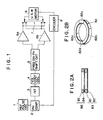
- Fig. 1 is a block diagram of an embodiment of the present invention
- Fig. 2A is a cross-sectional view schematically showing the structure of an ultrasonic wave motor
- Fig. 2B is a perspective view of a vibration member composed of a piezoelectric member and a resilient member.
- the capacitor C is charged, through the resistor R1, by the output voltage of the voltage follower 405.
- the oscillation frequency of the VCO 401 starts to elevate again, and, when it exceeds 4 x f H again, it is controlled to 4 x f H or below as explained above.
- the switch 7 When the switch 7 is closed in either direction in this state, the signal from the switch 411 to the multiplexer 412 is shifted to the low level, whereby the multiplexer 412 selects the output of the low-frequency discriminator 403 supplied through the inverter 407. Also since the input from the switch 411 to the 3-input OR gate 413 is shifted to the low level, an operation similar to that explained in relation to Fig. 10 is conducted when either one of the outputs of the frequency discriminators 402, 403 is shifted to the high-level state. Thus the oscillation frequency of the VCO 401 is controlled to a value corresponding to a predetermined revolution, within a frequency range of 4 x f L to 4 x f H .
Landscapes
- General Electrical Machinery Utilizing Piezoelectricity, Electrostriction Or Magnetostriction (AREA)
Abstract
a stator member having an electrostrictive member and a resilient member, and adapted to generate travelling vibration wave in the resilient member by excitation with the electrostrictive member;
a moving member maintained in pressure contact with the stator member and driven by the travelling vibration wave;
a reference pulse oscillator circuit for generating reference pulses of a frequency determined corresponding to a required moving speed of the moving member;
an encoder for generating pulses relating to the amount of movement of the moving member;
a phase difference signal generating circuit for generating a phase difference signal corresponding to the phase difference between the reference pulses from the reference pulse oscillator circuit and the output pulses of the encoder; and
AC voltage forming circuit for forming AC voltage signals to be supplied to the electrostrictive member, based on the phase difference signal.
Description
- The present invention relates to an ultrasonic wave motor in which a moving member is driven by travelling vibration wave generated in a resilient member by a piezoelectric member.
- As disclosed in the U.S. Patent 4,510,411, the ultrasonic wave motor utilizing travelling vibration wave generates travelling vibration wave in a resilient member by applying an AC voltage to a piezoelectric member attached to said resilient member and thereby causing bending vibration in said piezoelectric member, and drives a rotor by maintaining said rotor in pressure contact with said resilient member.
- The driving speed of such ultrasonic wave motor has been conventionally controlled by the frequency of the applied AC voltage in such a manner that the output voltage from a monitor electrode provided on the piezoelectric member remains at a predetermined level, or in such a manner that the phase difference between the output of the monitor electrode and the applied AC voltage becomes constant.
- However, such frequency control to obtain constant monitor voltage or phase difference is sometimes still unable to provide desired speed, due to change in load, fluctuation in the ambient conditions or fluctuation in the pressure mentioned above.
- On the other hand, in the field of DC motor, there is already well known the control by phase locked loop (PLL) for obtaining a desired revolution in stable manner. However, since the driving mechanism of the ultrasonic wave motor is different from that of the DC motor, the PLL circuit for DC motor cannot be immediately applied to the ultrasonic wave motor.
- The object of the present invention is to realize a speed control circuit of phase locked loop method suitable for the ultrasonic wave motor, thereby providing a driving device capable of stabilizing the drive speed of the ultrasonic wave motor, without being influenced for example by the ambient conditions.
- The above-mentioned object can be attained according to the present invention, by a driving device which is provided, as shown in Fig. 1 representing an embodiment of the present invention, with a reference pulse oscillator means 1 for generating reference pulses of a frequency corresponding to the predetermined revolution of an
ultrasonic wave motor 8, anencoder 9 for generating pulses in proportion to the amount of movement of a moving member, phase difference signal generating means 2 for generating a signal corresponding to the phase difference between the reference pulses from said reference pulse oscillator means 1 and the output pulses of theencoder 9, an integrator means 3 for integrating said phase difference signal, pulse generator means 4 for generating a pulse signal of a frequency corresponding to the output signal of said integrator means 3 within a range between an upper limit frequency and a lower limit frequency which are specific to theultrasonic wave motor 8, and AC voltage signal forming means 5, 6a, 6b for forming an AC voltage signal in response to said pulse signal. - In the above-explained circuit, pulses proportional to the moving speed of the moving member are generated by the
encoder 9, then there is obtained a signal corresponding to the phase difference between the reference pulses and the output pulses of the encoder, and said phase difference signal is integrated. Then pulses of a frequency corresponding to thus integrated signal are formed, and an AC voltage signal of said frequency is applied to the ultrasonic wave motor. Consequently the ultrasonic wave motor is driven at a predetermined revolution, even in the presence of changes in driving conditions such as ambient conditions or pressure. -
- Fig. 1 is a block diagram of an embodiment of the driving device for ultrasonic wave motor of the present invention;
- Figs. 2A and 2B are respectively a cross-sectional view and a perspective view schematically showing the structure of an ultrasonic wave motor;
- Fig. 3 is a chart showing the relation between drive frequency and drive speed of an ultrasonic wave motor;
- Fig. 4 is a schematic view showing the state of mounting of the encoder;
- Fig. 5 is a circuit diagram of a phase comparator and a loop filter;
- Fig. 6 is a timing chart of various input and output circuits in the circuit shown in Fig. 5;
- Fig. 7 is a chart showing the relation between the input voltage and the output frequency of a voltage-controlled oscillator;
- Fig. 8 is a circuit diagram of a frequency-dividing phase-shifting circuit;
- Fig. 9 is a timing chart of various signals therein; and
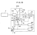
- Figs. 10 to 13 are block diagrams showing examples of a voltage-controlled oscillating circuit, utilizing a voltage-controlled oscillator having a frequency region exceeding the range from the lowest driving frequency to the highest driving frequency of the ultrasonic wave motor.
- Fig. 1 is a block diagram of an embodiment of the present invention, Fig. 2A is a cross-sectional view schematically showing the structure of an ultrasonic wave motor, and Fig. 2B is a perspective view of a vibration member composed of a piezoelectric member and a resilient member.
- At first the structure of the ultrasonic wave motor will be explained with reference to Figs. 2A and 2B. A
vibration member 83 is composed of aresilient member 81 and apiezoelectric member 82 adhered on a face thereof. Arotor 85 is maintained in pressure contact, across aslider 84, on the other face of thepiezoelectric member 82, and saidslider 84 androtor 85 constitute a rotatingmember 86. - The
piezoelectric member 82 is provided, on the surface thereof as shown in Fig. 2B, with fourelectrodes electrodes electrode 82c is grounded. Theelectrode 82d is used for obtaining a monitor signal. The structure and function of these components will not be explained further, as they are already known, for example in the U.S. Patent 4,510,411. - Such ultrasonic wave motor has frequency-speed characteristics as shown by a solid line C1 or a broken line C2 in Fig. 3. Thus, when the driving frequency is higher than the resonance frequency fM, the revolution increases as the driving frequency decreases. On the other hand, when the driving frequency is lower than the resonance frequency fM, the revolution decreases as the driving frequency decreases. In general, the speed control is considered possible between a maximum frequency fH and a minimum frequency fL which are higher than said resonance frequency fM. The lower limit frequency fL of the oscillation band of the voltage-controlled
oscillator 4 shown in Fig. 1 is so selected as to satisfy a condition fL > fM even when the resonance frequency fM varies for example by change in the load, fluctuation in the ambient conditions or change in the pressure. The maximum frequency fH corresponds to the lowest revolution of the ultrasonic wave motor, and is so selected as to provide a revolution sufficiently lower than the desired revolution. Also the minimum frequency fL corresponds to the highest revolution of the ultrasonic wave motor, and is so selected as to be higher than the resonance frequency even in the presence of a fluctuation in the load in the course of rotation of the ultrasonic wave motor at the desired revolution. The solid line C1 shows the frequency-speed characteristics of theultrasonic wave motor 8 under a certain ambient condition (hereinafter called 1st driving condition), and the broken line C2 indicates said characteristics under a different ambient condition (hereinafter called 2nd driving condition). - In the present embodiment, as shown in Fig. 4, a
shaft 85a extending from therotor 85 is coupled with arotary encoder 9 throughgears rotary encoder 9 generates pulses of a frequency proportional to the revolution of therotor 85. - Now referring to Fig. 1, there are shown a reference pulse oscillator 1 for generating reference pulses of a frequency corresponding to a revolution N1 to be explained later; a
phase comparator 2 for comparing the phase of the output pulses from theencoder 9 with that of the reference pulses and generating a signal corresponding to the phase difference therebetween; anintegrator 3, called a loop filter, for integrating the output signal of thephase comparator 2; a voltage-controlled oscillator (VCO) 4 for generating pulses of a frequency corresponding to the output voltage of saidintegrator 3; a frequency-dividing phase-shiftingcircuit 5 for dividing the frequency of pulses from theVCO 4 and generating signals of a mutual phase difference of π/2; knownpower amplifiers circuit 5 for supply to theelectrodes piezoelectric member 82 of theultrasonic wave motor 8; and switches 7 for controlling the input signals to theultrasonic wave motor 8, thereby switching the rotating direction thereof, or stopping the motor in the open state. - The details of the
phase comparator 2 and theintegrator 3 are shown in Fig. 5. - The
phase comparator 2 is composed of JK-flip-flops encoder 9 and the reference pulses; aNAND gate 22;NOR gates integrator 3 is composed of aresistor 31 and acapacitor 32, constituting a lag filter. - Now the functions of the
phase comparator 2 and theintegrator 3 will be explained with reference to Fig. 6. - In Fig. 6, (a) shows the reference pulses from the reference pulse oscillator 1, (b) output signal of the
encoder 9, (c) output signal of thephase comparator 2, and (d) output signal of theloop filter 3. - When the phase of the encoder output pulses is delayed from that of the reference pulses as shown in the section I, the
MOSFET 28B is turned on from the upshift of the reference pulse to that of the encoder output pulse, namely for a period corresponding to the delay in phase as shown in (c), whereby the output of thephase comparator 2 becomes zero. At the upshift of the encoder output pulse, the MOSFET's 28A, 28B are turned off, whereby the output of thephase comparator 2 assumes a high-impedance state as indicated by a chain line in (c). As shown in (d), the output of theloop filter 3 descends after theMOSFET 28B is turned on, but is retained when the output of thephase comparator 2 assumes the high impedance state by the turning-off of theMOSFET 28B. - In the section II, the reference pulses and the encoder output pulses are of a same phase, whereby the MOSFET's 28A, 28B are maintained off, and the output of the
loop filter 3 remains constant as shown in (d). - In the section III, the reference pulses are delayed in phase with respect to the encoder output pulses. whereby the
MOSFET 28A is turned on from the upshift of the encoder output pulse to the downshift of the reference pulse, and thephase comparator 2 releases a voltage Vcc as shown in (c). Consequently the output voltage of theloop filter 3 increases. - In the section IV, the frequency of the encoder output pulses is lower than that of the reference pulses, whereby the output of the
loop filter 3 decreases. - In the section V, the frequency of the encoder output pulses is higher than that of the reference pulses, whereby the output of the
loop filter 3 increases. - Thus the output of the
loop filter 3 decreases when the reference pulses are advanced in phase or are of a higher frequency compared with the encoder output pulses, and vice versa. Also said output does not change if the reference pulses and the encoder output pulses are of a same phase and a same frequency. - Fig. 7 shows the relationship between the input voltage and the output frequency of the
VCO 4, wherein said input voltage is the output voltage of theloop filter 3. Afrequency 4 x fL is released in response to the minimum output voltage of 0 V from theloop filter 3, and afrequency 4 x fH is released in response to the maximum output voltage Vcc from theloop filter 3. - The frequency-dividing phase-shifting
circuit 5 is composed, as shown in Fig. 8 of two D-flip-flops flop 51 is connected to the data input terminal D of the flip-flop 52 while the inverted set output terminalQ is connected to the data input terminal D of the flip-flop 51. Consequently, as shown in Fig. 9, saidcircuit 5 divides the output frequency of theVCO 4 into 1/4 and generates signals having a mutually phase difference of π/2. - In the following there will be explained the function of the driving device for ultrasonic wave motor of the present invention.
- Let us consider a state in which the
ultrasonic wave motor 8 is driven with a revolution N1 by the application of an AC voltage of a driving frequency f1 to the piezoelectric member of said motor under the lst driving condition represented by the curve C1 in Fig. 3. If the driving condition changes to the 2nd one, the revolution of themotor 8 changes to N2 defined by the curve C2. - The present invention is to effect PLL speed control in such case. thereby maintaining the
ultrasonic wave motor 8 at the revolution N1 even after the change from the 1st to the 2nd driving condition. - If the
ultrasonic wave motor 8 and theencoder 9 rotate with a 1 : 1 speed ratio, the frequency of the encoder output pulses at the revolution N1 of themotor 8 can be represented by:
FE x
wherein FE is the number of output pulses of theencoder 9 per turn thereof. - Thus the frequency of the reference pulses of the reference pulse oscillator 1 is selected at a value determined by (1).
- When the
switches 7 are in a neutral position shown in Fig. 1 and theultrasonic wave motor 8 is stopped, the frequency of the output pulses of theencoder 9 is 0 Hz. In this state thephase comparator 2 receives the reference pulses, and the output voltage of theloop filter 3 decreases with time to reach 0 V after a predetermined time. Consequently the output of theVCO 4 becomes equal to 4 x fL as shown in Fig. 7. When theswitches 7 are closed in either direction, the set output terminals Q of the flip-flops circuit 5 release signals, as shown by (b) and (c) in Fig. 9, having a frequency equal to four times that of the input signal from theVCO 4 and having a mutual phase difference of π/2. Consequently theultrasonic wave motor 8 receives the AC voltage of a frequency fL and starts rotation toward the maximum resolution. - In the course of gradual increase of revolution of the
motor 8, while said revolution is lower than N1, the frequency of the encoder output pulses is lower than that of the reference pulses, whereby thephase comparator 2 decreases the output voltage of theloop filter 3 as explained above. Consequently the output voltage of theloop filter 3 becomes approximately zero, whereby the output frequency of theVCO 4 becomes equal to 4 x fL to apply the AC voltage of a frequency fL, corresponding to the maximum revolution, to theultrasonic wave motor 8. Thus the revolution of themotor 8 increases with time. When the revolution exceeds N1, the frequency of the encoder output pulses becomes higher than that of the reference pulses, whereby thephase comparator 2 increases the output voltage of theloop filter 3 as explained above. Consequently the output frequency of theVCO 4 increases to elevate the driving frequency, thereby reducing the revolution of theultrasonic wave motor 8. Repetition of the above-explained cycles brings the driving frequency to f₁ providing the target revolution N1. The rate of convergence to said frequency can be suitably regulated by the time constant of said loop filter. - Then, if the driving condition varies from the 1st to the 2nd one due to a fluctuation in the load or in the pressure, the frequency-revolution characteristics of the
ultrasonic wave motor 8 changes from C1 to C2 shown in Fig. 3, whereby the revolution at the driving frequency f₁ increases toward N2 ( > N1). Consequently the frequency of the encoder output pulses becomes larger than that of the reference pulses, whereby thephase comparator 2 elevates the output voltage of theloop filter 3. As the result of output frequency of theVCO 4 increases, and the driving frequency varies toward the maximum frequency fH. Through this operation the revolution of themotor 8 is lowered, and the driving frequency converges to f₂ providing the revolution N1. - As explained in the foregoing, the PLL speed control circuit of the present invention maintains the revolution of the
ultrasonic wave motor 8 at a constant value, regardless of the change for example in the ambient condition or in the pressure. - In the above-explained embodiment, the reference pulse oscillator means is formed by the reference pulse oscillator 1, phase difference signal generating means by the
phase comparator 2, integrating means by theloop filter 3, pulse generating means by theVCO 4, and AC voltage signal forming means by the frequency-dividing phase-shiftingcircuit 5 andpower amplifiers - The
loop filter 3 is composed of a lag filter in the foregoing explanation, but it may also be composed of a lag lead filter or an active filter. Also the phase comparator may be composed of a bi-directional shift register instead of JK-flip-flops. Also the encoder may be of any type or structure as long as it is capable of generating pulses corresponding to the speed of the moving member. - The
VCO 4 employed in the above-explained embodiment is so designed to generate pulse signals of afrequency 4 x fL or 4 x fH respectively in response to the input voltage of 0 V or Vcc. If the VCO itself does not have such characteristics, there may be obtained oscillation with a range from 4 x fL to 4 x fH by a voltage-controlled oscillator circuit explained in the following. - (1) Fig. 10 illustrates an embodiment of the voltage-control oscillator circuit capable of defining the upper and lower limits of the oscillation frequency by controlling the output voltage of the
loop filter 3, wherein a voltage-controlled oscillator circuit (pulse generating means) 400A is composed of a VCO 400 and a peripheral circuit for limiting the oscillation frequency thereof. TheVCO 401 itself generates pulses of a frequency lower than 4 x fL in response to an input voltage of 0 V, and pulses of a frequency higher than 4 x fH in response to an input voltage Vcc. Ahigh frequency discriminator 402 releases a high-level signal when the output frequency of theVCO 401 is higher than 4 x fH, or a low-level signal when said output frequency is equal to or lower than 4 x fH. Alow frequency discriminator 403 releases a high-level signal or a low-level signal respectively when the output of theVCO 401 is of a lower frequency than 4 x fL, or equal to or higher than 4 x fL. Ananalog switch 404 is closed when the output of theVCO 401 is within a frequency range of 4 x fL to 4 x fH or otherwise opened, according to the output signals of said high-frequency discriminator 402 and of the low-frequency discriminator 403. There are also shown a knownvoltage follower 405, an ORgate 406 for forming the logic sum of the output signals of thefrequency discriminators analog switch 404, aninverter 407 for inverting the output of the low-frequency discriminator 403, a low-pass filter 408 composed of a resistor R1 and a capacitor C and having a time constant sufficiently smaller than that of theloop filter 3, atransistor 409 to be turned on by the output signal of the low-frequency discriminator 403 through theinverter 407 when theVCO 401 releases a frequency lower than 4 x fL, atransistor 410 to be turned on by the output signal of the high-frequency discriminator 402 when theVCO 401 releases a frequency higher than 4 x fH, and resistors R2 - R5. - In the following there will be explained the function of the voltage-controlled
oscillator circuit 400A, consisting of theVCO 401 and the peripheral circuits. - When the
VCO 401 oscillates within the frequency range of 4 x fL to 4 x fH in the course of function of theultrasonic wave motor 8, theanalog switch 404 is closed and thetransistors loop filter 3, transmitted through thevoltage follower 405, is supplied to theVCO 401 through the low-pass filter 408, whereby theVCO 401 releases pulses of a frequency corresponding to said input voltage. - If the oscillation frequency of the
VCO 401 becomes higher than 4 x fH due to the increase of the output voltage of theloop filter 3 in this state, the high-frequency discriminator 402 releases a high-level output to open theanalog switch 404, thereby intercepting the output signal of thevoltage follower 405 and turning on thetransistor 410. Since thetransistor 409 is turned off, the capacitor C is discharged through the resistor R5, thereby reducing the input voltage to theVCO 401 and reducing the oscillation frequency thereof. When the output frequency of theVCO 401 becomes lower than 4 x fH, the output of the high-frequency discriminator 402 is inverted to the low level state thereby closing theanalog switch 404 and turning off thetransistor 410. Thus the capacitor C is charged, through the resistor R1, by the output voltage of thevoltage follower 405. In response the oscillation frequency of theVCO 401 starts to elevate again, and, when it exceeds 4 x fH again, it is controlled to 4 x fH or below as explained above. - On the other hand, if the oscillation frequency of the
VCO 401 is lower than 4 x fL due to the low output voltage of theloop filter 3, the low-frequency discriminator 403 releases a high-level output to open theanalog switch 404 and to turn on thetransistor 409. Since thetransistor 410 is turned off, the capacitor C is charged through the resistor R3, thereby elevating the input voltage to theVCO 401 and increasing the oscillation frequency thereof. When said oscillation frequency becomes equal to or higher than 4 x fL, the output of the low-frequency discriminator 403 is shifted to the low level state, thereby closing theanalog switch 404 and turning off thetransistor 409. Thus the capacitor C is charged by the output voltage of thevoltage follower 405, whereby the input voltage of the theVCO 401 continues to rise, and the oscillation frequency thereof is maintained at 4 x fL or higher. - The voltage-controlled
oscillation circuit 400A including the peripheral circuit explained above is thus capable of maintaining the oscillation frequency within a range from 4 x fL to 4 x fH, even utilizing a VCO of which oscillation frequency range does not match the above-mentioned range. - (2) In the above-explained embodiment shown in Fig. 10, if the
switch 7 is closed simultaneously with the activation of the driving circuit for theultrasonic wave motor 8, the oscillation frequency of theVCO 401 at the starting of the motor is 4 x fL so that themotor 8 is started with the frequency corresponding to the maximum revolution and is gradually controlled to the target revolution. On the other hand, for starting the motor with the minimum revolution, there can be employed a voltage-controlledoscillator circuit 400B shown in Fig. 11, in which same components as those in Fig. 10 are represented by same numbers. In the following there will principally be explained the differences from the foregoing embodiment. - A
switch 411 is linked with theswitch 7 shown in Fig. 1, and is in a neutral position when theultrasonic wave motor 8 is stopped. Amultiplexer 412 selects the output of theinverter 407 or that of the high-frequency discriminator 402, for supply to the base of thetransistor 409. When saidswitch 411 is in the neutral positions a high-level signal is supplied through a resistor R6 to the control terminal of saidmultiplexer 412, which in response selects the output of the high-frequency discriminator 402. On the other hand, when theswitch 411 is closed, a low-level signal is supplied to the control terminal of themultiplexer 412, which in response selects the output signal of theinverter 407. A 3-input ORgate 413 receives the outputs of theswitch 411 and the high-and low-frequency discriminators analog switch 404. - When the
ultrasonic wave motor 8 is stopped by the open state of theswitch 7, a high-level signal from theswitch 411 is supplied, through theOR gate 413, to the control terminal of theanalog switch 404, which is in response maintained open. On the other hand, in response to said high-level signal, themultiplexer 412 selects the high-frequency discriminator 402. In this state, if the oscillation frequency of theVCO 401 is higher than 4 x fH, the high-frequency discriminator 402 releases a high-level signal to turn off thetransistor 409 and turn on thetransistor 410. Thus the capacitor C is discharged through the resistor R5, whereby the input voltage of theVCO 401 decreases and the oscillation frequency thereof also decreases. When it becomes equal to or lower than 4 x fH, the output of the high-frequency discriminator 402 is shifted to the low-level state to turn off thetransistor 410 and to turn on thetransistor 409, whereby the capacitor C is charged through the resistor R3. Thus the input voltage to theVCO 401 is elevated and the oscillation frequency thereof increases. When it again exceeds 4 x fH, the output of thefrequency discriminator 402 is inverted and the oscillation frequency decreases. By the repetition of the above-explained functions, theVCO 401 oscillates at 4 x fH when theultrasonic wave motor 8 is stopped. - When the
switch 7 is closed in either direction in this state, the signal from theswitch 411 to themultiplexer 412 is shifted to the low level, whereby themultiplexer 412 selects the output of the low-frequency discriminator 403 supplied through theinverter 407. Also since the input from theswitch 411 to the 3-input ORgate 413 is shifted to the low level, an operation similar to that explained in relation to Fig. 10 is conducted when either one of the outputs of thefrequency discriminators VCO 401 is controlled to a value corresponding to a predetermined revolution, within a frequency range of 4 x fL to 4 x fH. -
- (1) Fig. 12 is an embodiment of the voltage-controlled
oscillator circuit 400C for controlling the input voltage of theloop filter 3, corresponding to Fig. 10. In Fig. 12, same components as those in Fig. 10 are represented by same numbers. - The
circuit 400C is formed by inserting the components of the circuit shown in Fig. 10, except for thevoltage follower 405 and the low-pass filter 408, in the input side of theloop filter 3 as shown in Fig. 12. - When the oscillation frequency of the
VCO 401 exceeds 4 x fH, theanalog switch 404 is opened and thetransistor 410 is turned on, whereby acapacitor 32 is discharged through the resistor R5. Thus the input voltage to theVCO 401 is lowered to reduce the oscillation frequency thereof. When the oscillation frequency becomes equal to or lower than 4 x fH, theanalog switch 404 is closed and thetransistor 410 is turned off, whereby thecapacitor 32 is charged by the output voltage of thephase comparator 2 to elevate the input voltage to theVCO 401 again, thereby increasing the oscillation frequency thereof. By reception of the above-explained operations, the oscillation frequency of theVCO 401 is controlled to 4 x fH. - When the
VCO 401 oscillates at a frequency equal to or lower than 4 x fL, the components are similar controlled by the output signal of the low-frequency discriminator 403, whereby the oscillation frequency of theVCO 401 is controlled to 4 x fL. - (2) Fig. 13 shows another embodiment corresponding to Fig. 11, wherein same components as those in Fig. 11 are represented by same numbers, and different points only will be explained in the following.
- The voltage-controlled
oscillator circuit 400D is formed by inserting the components shown in Fig. 11, except for thevoltage follower 405 and the low-pass filter 408, into the input side of theloop filter 3, as shown in Fig. 13. - When the
switch 7 is off, theswitch 411 releases a high-level signal whereby theanalog switch 404 is opened and themultiplexer 412 selects the high-frequency discriminator 402. If the output of thefrequency discriminator 402 is at the low level state, thetransistor 409 is turned on while thetransistor 410 is turned off. Consequently thecapacitor 32 of theloop filter 3 is charged through the resistor R3, thus elevating the input voltage to theVCO 401. When the oscillation frequency thereof exceeds 4 x fH, thetransistor 409 is turned off while thetransistor 410 is turned on to discharge thecapacitor 32 through the resistor R5, thereby reducing the input voltage to theVCO 401. When the oscillation frequency becomes equal to or less than 4 x fH, thecapacitor 32 is charged again to elevate the input voltage of theVCO 401, thereby increasing the oscillation frequency thereof. By the repetition of such operations, the oscillation frequency of theVCO 401 is controlled to 4 x fH when theultrasonic wave motor 8 is stopped, when theswitch 7 is closed, themotor 8 is started with the minimum revolution. - The present invention is naturally applicable to the linear ultrasonic wave motor.
- As explained in the foregoing, the present invention allows to control the ultrasonic wave motor with a phase-locked loop speed control circuit, and to obtain a predetermined revolution in stable manner even in the presence of fluctuation in the ambient condition or in the pressure.
Claims (13)
a stator member having an electrostrictive member and a resilient member and adapted to generate travelling vibration wave in said resilient member by excitation with said electrostrictive member;
a moving member maintained in pressure contact with said stator member and driven by said travelling vibration wave;
reference pulse oscillator means for generating reference pulses of a frequency determined corresponding to a requested moving speed of said moving member;
an encoder for generating pulses related to the amount of movement of said moving member;
phase difference signal generating means for generating a phase difference signal corresponding to the phase difference between the reference pulses generated by said reference pulse oscillator means and the output pulses of said encoder; and
AC voltage forming means for forming AC voltage signals to be applied to said electrostrictive member based on said phase difference signal.
a stator member having an electrostrictive member and a resilient member, and adapted to generate travelling vibration wave in said resilient member by excitation with said electrostrictive member;
a moving member maintained in pressure contact with said stator member and driven by said travelling vibration wave;
reference pulse oscillator means for generating reference pulses of a frequency determined corresponding to a requested moving speed of said moving member;
an encoder for generating pulses related to the amount of movement of said moving member;
phase difference signal generating means for generating a phase difference signal corresponding to the difference in frequency and in phase between the reference pulses generated by said reference pulse oscillator means and the output pulses of said encoder; and
AC voltage forming means for forming AC voltage signals to be applied to said electrostrictive member based on said phase difference signal.
Applications Claiming Priority (2)
| Application Number | Priority Date | Filing Date | Title |
|---|---|---|---|
| JP153114/89 | 1989-06-15 | ||
| JP1153114A JP2890484B2 (en) | 1989-06-15 | 1989-06-15 | Ultrasonic motor drive |
Publications (3)
| Publication Number | Publication Date |
|---|---|
| EP0403298A2 true EP0403298A2 (en) | 1990-12-19 |
| EP0403298A3 EP0403298A3 (en) | 1991-10-16 |
| EP0403298B1 EP0403298B1 (en) | 1996-01-17 |
Family
ID=15555279
Family Applications (1)
| Application Number | Title | Priority Date | Filing Date |
|---|---|---|---|
| EP90306539A Expired - Lifetime EP0403298B1 (en) | 1989-06-15 | 1990-06-15 | Driving device for ultrasonic wave motor |
Country Status (4)
| Country | Link |
|---|---|
| US (1) | US5625263A (en) |
| EP (1) | EP0403298B1 (en) |
| JP (1) | JP2890484B2 (en) |
| DE (1) | DE69024855T2 (en) |
Cited By (6)
| Publication number | Priority date | Publication date | Assignee | Title |
|---|---|---|---|---|
| US5198732A (en) * | 1991-08-22 | 1993-03-30 | Mitsubishi Jukogyo Kabushiki Kaisha | Rotation control system for ultrasonic motor |
| EP0678861A2 (en) * | 1994-04-20 | 1995-10-25 | Canon Kabushiki Kaisha | Optical information recording and/or reproducing apparatus and method with vibration wave driving device or vibration driven motor device |
| EP0702419A1 (en) * | 1994-09-19 | 1996-03-20 | Magneti Marelli France | Improved transducer, in particular a piezoelectric motor |
| EP0831540A1 (en) * | 1994-07-20 | 1998-03-25 | Matsushita Electric Industrial Co., Ltd. | A method for driving an ultrasonic motor |
| EP0926808A2 (en) * | 1997-12-12 | 1999-06-30 | Canon Kabushiki Kaisha | A driving apparatus for a vibration type actuator |
| CN102499878A (en) * | 2011-11-07 | 2012-06-20 | 江南大学 | Pocket type ultrasonic acupoint massager and operating circuit thereof |
Families Citing this family (5)
| Publication number | Priority date | Publication date | Assignee | Title |
|---|---|---|---|---|
| US6005328A (en) * | 1989-06-15 | 1999-12-21 | Nikon Corporation | Driving device and method for ultrasonic wave motor |
| EP0442469B1 (en) * | 1990-02-14 | 1995-07-26 | Nikon Corporation | Driving device for ultrasonic wave motor |
| JPH03289369A (en) * | 1990-04-02 | 1991-12-19 | Mitsubishi Heavy Ind Ltd | Speed controller for ultrasonic motor |
| JPH0879896A (en) * | 1994-09-06 | 1996-03-22 | Canon Inc | Speaker |
| JP4541497B2 (en) | 2000-05-08 | 2010-09-08 | キヤノンプレシジョン株式会社 | Vibration wave motor drive control device, drive control method, and storage medium |
Citations (1)
| Publication number | Priority date | Publication date | Assignee | Title |
|---|---|---|---|---|
| JPS63206171A (en) * | 1987-02-19 | 1988-08-25 | Nikon Corp | Drive controlling circuit for ultrasonic wave motor |
Family Cites Families (19)
| Publication number | Priority date | Publication date | Assignee | Title |
|---|---|---|---|---|
| JPS59111609A (en) * | 1982-12-17 | 1984-06-27 | Nippon Kogaku Kk <Nikon> | Lens barrel |
| JPS59204477A (en) * | 1983-05-04 | 1984-11-19 | Nippon Kogaku Kk <Nikon> | Surface wave motor utilizing supersonic wave vibration |
| US4692649A (en) * | 1985-03-01 | 1987-09-08 | Canon Kabushiki Kaisha | Driving circuit of a vibration wave motor |
| US4727276A (en) * | 1985-03-26 | 1988-02-23 | Canon Kabushiki Kaisha | Driving circuit for vibration wave motor |
| JPH07108105B2 (en) * | 1985-09-04 | 1995-11-15 | 松下電器産業株式会社 | Ultrasonic motor driving method |
| US4743788A (en) * | 1985-11-20 | 1988-05-10 | Nippon Kogaku K. K. | Input frequency control device for surface acoustic wave motor |
| US4713571A (en) * | 1986-01-23 | 1987-12-15 | Canon Kabushiki Kaisha | Driving circuit of a vibration wave motor |
| US4794294A (en) * | 1986-06-12 | 1988-12-27 | Canon Kabushiki Kaisha | Vibration wave motor |
| JPH078153B2 (en) * | 1986-07-14 | 1995-01-30 | キヤノン株式会社 | Vibration wave motor device |
| US4812699A (en) * | 1986-11-11 | 1989-03-14 | Nikon Corporation | Drive control device in an ultrasonic vibration motor |
| US5136215A (en) * | 1986-12-15 | 1992-08-04 | Canon Kabushiki Kaisha | Driving circuit for vibration wave motor |
| JPS63178774A (en) * | 1987-01-19 | 1988-07-22 | Canon Inc | Driving circuit for oscillatory wave motor |
| JP2586082B2 (en) * | 1987-02-09 | 1997-02-26 | 株式会社ニコン | Power frequency optimization device for ultrasonic motor |
| US5159253A (en) * | 1987-02-24 | 1992-10-27 | Canon Kabushiki Kaisha | Control device for a vibration wave motor |
| JPH01185174A (en) * | 1988-01-11 | 1989-07-24 | Canon Inc | Drive circuit for oscillatory wave motor |
| JPH01234073A (en) * | 1988-03-14 | 1989-09-19 | Olympus Optical Co Ltd | Drive circuit for vibration wave motor |
| JP2637467B2 (en) * | 1988-05-06 | 1997-08-06 | キヤノン株式会社 | Vibration type actuator device |
| JPH0710189B2 (en) * | 1988-05-30 | 1995-02-01 | キヤノン株式会社 | Vibration wave motor drive circuit |
| US4879528A (en) * | 1988-08-30 | 1989-11-07 | Olympus Optical Co., Ltd. | Ultrasonic oscillation circuit |
-
1989
- 1989-06-15 JP JP1153114A patent/JP2890484B2/en not_active Expired - Lifetime
-
1990
- 1990-06-15 EP EP90306539A patent/EP0403298B1/en not_active Expired - Lifetime
- 1990-06-15 DE DE69024855T patent/DE69024855T2/en not_active Expired - Fee Related
-
1995
- 1995-02-28 US US08/396,324 patent/US5625263A/en not_active Expired - Fee Related
Patent Citations (1)
| Publication number | Priority date | Publication date | Assignee | Title |
|---|---|---|---|---|
| JPS63206171A (en) * | 1987-02-19 | 1988-08-25 | Nikon Corp | Drive controlling circuit for ultrasonic wave motor |
Non-Patent Citations (1)
| Title |
|---|
| PATENT ABSTRACTS OF JAPAN vol. 12, no. 493 (E-697)(3340) 22 December 1988, & JP-A-63 206171 (NICON CORP.) 25 August 1988, * |
Cited By (17)
| Publication number | Priority date | Publication date | Assignee | Title |
|---|---|---|---|---|
| EP0791969A1 (en) * | 1991-08-22 | 1997-08-27 | Mitsubishi Jukogyo Kabushiki Kaisha | Control system for ultrasonic motor |
| EP0537384A1 (en) * | 1991-08-22 | 1993-04-21 | Mitsubishi Jukogyo Kabushiki Kaisha | Rotation control system for ultrasonic motor |
| US5198732A (en) * | 1991-08-22 | 1993-03-30 | Mitsubishi Jukogyo Kabushiki Kaisha | Rotation control system for ultrasonic motor |
| EP0975028A3 (en) * | 1994-04-20 | 2000-04-12 | Canon Kabushiki Kaisha | Vibration driven motor |
| US5990596A (en) * | 1994-04-20 | 1999-11-23 | Canon Kabushiki Kaisha | Optical information recording and/or reproducing apparatus and method with vibration wave driving device or vibration driven motor device |
| EP0678861A3 (en) * | 1994-04-20 | 1996-05-01 | Canon Kk | Optical information recording and/or reproducing apparatus and method with vibration wave driving device or vibration driven motor device. |
| EP0678861A2 (en) * | 1994-04-20 | 1995-10-25 | Canon Kabushiki Kaisha | Optical information recording and/or reproducing apparatus and method with vibration wave driving device or vibration driven motor device |
| EP0975028A2 (en) * | 1994-04-20 | 2000-01-26 | Canon Kabushiki Kaisha | Vibration driven motor |
| US5805540A (en) * | 1994-04-20 | 1998-09-08 | Canon Kabushiki Kaisha | Optical information recording and/or reproducing apparatus and method with vibration wave driving device or vibration driven motor device |
| EP0831540A1 (en) * | 1994-07-20 | 1998-03-25 | Matsushita Electric Industrial Co., Ltd. | A method for driving an ultrasonic motor |
| EP0702418A1 (en) * | 1994-09-19 | 1996-03-20 | Magneti Marelli France | Progressive mechanical wave transducer |
| EP0702419A1 (en) * | 1994-09-19 | 1996-03-20 | Magneti Marelli France | Improved transducer, in particular a piezoelectric motor |
| EP0926808A2 (en) * | 1997-12-12 | 1999-06-30 | Canon Kabushiki Kaisha | A driving apparatus for a vibration type actuator |
| EP0926808A3 (en) * | 1997-12-12 | 2000-11-22 | Canon Kabushiki Kaisha | A driving apparatus for a vibration type actuator |
| EP1638197A2 (en) * | 1997-12-12 | 2006-03-22 | Canon Kabushiki Kaisha | A driving apparatus of a vibration type actuator |
| EP1638197A3 (en) * | 1997-12-12 | 2006-05-31 | Canon Kabushiki Kaisha | A driving apparatus of a vibration type actuator |
| CN102499878A (en) * | 2011-11-07 | 2012-06-20 | 江南大学 | Pocket type ultrasonic acupoint massager and operating circuit thereof |
Also Published As
| Publication number | Publication date |
|---|---|
| DE69024855D1 (en) | 1996-02-29 |
| EP0403298B1 (en) | 1996-01-17 |
| JPH0318282A (en) | 1991-01-25 |
| JP2890484B2 (en) | 1999-05-17 |
| EP0403298A3 (en) | 1991-10-16 |
| DE69024855T2 (en) | 1996-07-11 |
| US5625263A (en) | 1997-04-29 |
Similar Documents
| Publication | Publication Date | Title |
|---|---|---|
| EP0403298A2 (en) | Driving device for ultrasonic wave motor | |
| US5126695A (en) | Semiconductor integrated circuit device operated with an applied voltage lower than required by its clock oscillator | |
| US5432693A (en) | Digital pulse width modulator circuit with proportional dither | |
| US5734236A (en) | Drive device for a vibration actuator having a control circuit to control charge and discharge of an electromechanical conversion element | |
| GB2183371A (en) | Vibration wave motor control | |
| JPH01303074A (en) | Driving circuit for oscillatory motor | |
| KR960006234A (en) | How to drive an ultrasonic motor | |
| US5702426A (en) | Automatic adjustment of electrical signal parameters | |
| US5159223A (en) | Driving apparatus for ultrasonic motor | |
| US6005328A (en) | Driving device and method for ultrasonic wave motor | |
| US5010222A (en) | Driving device for ultrasonic wave motor | |
| EP1576732A2 (en) | A sawtooth wave generating apparatus, a method of generating sawtooth wave, a constant current circuit, and a method of adjusting amount of current from the same | |
| JPH08308267A (en) | Drive device for ultrasonic motor | |
| JPH09163767A (en) | Driver of vibration actuator | |
| JP3140615B2 (en) | Driving method and driving circuit for ultrasonic motor | |
| US6633203B1 (en) | Method and apparatus for a gated oscillator in digital circuits | |
| JP2938628B2 (en) | Ultrasonic motor drive circuit | |
| JP4072243B2 (en) | Drive circuit for vibration actuator | |
| JP2819437B2 (en) | Ultrasonic motor drive controller | |
| JPH03203575A (en) | Ultrasonic motor device | |
| JPH04210787A (en) | Drive controller for ultrasonic motor | |
| KR100267710B1 (en) | Digital frequency phase control apparatus for driving ultrasonic motor | |
| KR100248018B1 (en) | Speed control circuit of an ultrasonic motor | |
| JPH06224691A (en) | Resistance circuit and filter circuit using the same | |
| EP1277280A1 (en) | Method and apparatus for a gated oscillator in digital circuits |
Legal Events
| Date | Code | Title | Description |
|---|---|---|---|
| PUAI | Public reference made under article 153(3) epc to a published international application that has entered the european phase |
Free format text: ORIGINAL CODE: 0009012 |
|
| AK | Designated contracting states |
Kind code of ref document: A2 Designated state(s): DE FR GB |
|
| PUAL | Search report despatched |
Free format text: ORIGINAL CODE: 0009013 |
|
| AK | Designated contracting states |
Kind code of ref document: A3 Designated state(s): DE FR GB |
|
| 17P | Request for examination filed |
Effective date: 19920402 |
|
| 17Q | First examination report despatched |
Effective date: 19940809 |
|
| GRAA | (expected) grant |
Free format text: ORIGINAL CODE: 0009210 |
|
| AK | Designated contracting states |
Kind code of ref document: B1 Designated state(s): DE FR GB |
|
| REF | Corresponds to: |
Ref document number: 69024855 Country of ref document: DE Date of ref document: 19960229 |
|
| ET | Fr: translation filed | ||
| PLBE | No opposition filed within time limit |
Free format text: ORIGINAL CODE: 0009261 |
|
| STAA | Information on the status of an ep patent application or granted ep patent |
Free format text: STATUS: NO OPPOSITION FILED WITHIN TIME LIMIT |
|
| 26N | No opposition filed | ||
| REG | Reference to a national code |
Ref country code: GB Ref legal event code: IF02 |
|
| PGFP | Annual fee paid to national office [announced via postgrant information from national office to epo] |
Ref country code: DE Payment date: 20070607 Year of fee payment: 18 |
|
| PGFP | Annual fee paid to national office [announced via postgrant information from national office to epo] |
Ref country code: GB Payment date: 20070613 Year of fee payment: 18 |
|
| PGFP | Annual fee paid to national office [announced via postgrant information from national office to epo] |
Ref country code: FR Payment date: 20070608 Year of fee payment: 18 |
|
| GBPC | Gb: european patent ceased through non-payment of renewal fee |
Effective date: 20080615 |
|
| REG | Reference to a national code |
Ref country code: FR Ref legal event code: ST Effective date: 20090228 |
|
| PG25 | Lapsed in a contracting state [announced via postgrant information from national office to epo] |
Ref country code: DE Free format text: LAPSE BECAUSE OF NON-PAYMENT OF DUE FEES Effective date: 20090101 |
|
| PG25 | Lapsed in a contracting state [announced via postgrant information from national office to epo] |
Ref country code: GB Free format text: LAPSE BECAUSE OF NON-PAYMENT OF DUE FEES Effective date: 20080615 |
|
| PG25 | Lapsed in a contracting state [announced via postgrant information from national office to epo] |
Ref country code: FR Free format text: LAPSE BECAUSE OF NON-PAYMENT OF DUE FEES Effective date: 20080630 |