EP0402784A2 - Method of manufacturing a CMOS semiconductor device - Google Patents
Method of manufacturing a CMOS semiconductor device Download PDFInfo
- Publication number
- EP0402784A2 EP0402784A2 EP90110875A EP90110875A EP0402784A2 EP 0402784 A2 EP0402784 A2 EP 0402784A2 EP 90110875 A EP90110875 A EP 90110875A EP 90110875 A EP90110875 A EP 90110875A EP 0402784 A2 EP0402784 A2 EP 0402784A2
- Authority
- EP
- European Patent Office
- Prior art keywords
- film
- mos transistor
- channel mos
- type impurity
- polysilicon film
- Prior art date
- Legal status (The legal status is an assumption and is not a legal conclusion. Google has not performed a legal analysis and makes no representation as to the accuracy of the status listed.)
- Granted
Links
Images


Classifications
-
- H—ELECTRICITY
- H10—SEMICONDUCTOR DEVICES; ELECTRIC SOLID-STATE DEVICES NOT OTHERWISE PROVIDED FOR
- H10D—INORGANIC ELECTRIC SEMICONDUCTOR DEVICES
- H10D84/00—Integrated devices formed in or on semiconductor substrates that comprise only semiconducting layers, e.g. on Si wafers or on GaAs-on-Si wafers
- H10D84/01—Manufacture or treatment
- H10D84/0123—Integrating together multiple components covered by H10D12/00 or H10D30/00, e.g. integrating multiple IGBTs
- H10D84/0126—Integrating together multiple components covered by H10D12/00 or H10D30/00, e.g. integrating multiple IGBTs the components including insulated gates, e.g. IGFETs
- H10D84/0165—Integrating together multiple components covered by H10D12/00 or H10D30/00, e.g. integrating multiple IGBTs the components including insulated gates, e.g. IGFETs the components including complementary IGFETs, e.g. CMOS devices
- H10D84/0172—Manufacturing their gate conductors
- H10D84/0177—Manufacturing their gate conductors the gate conductors having different materials or different implants
-
- H—ELECTRICITY
- H10—SEMICONDUCTOR DEVICES; ELECTRIC SOLID-STATE DEVICES NOT OTHERWISE PROVIDED FOR
- H10D—INORGANIC ELECTRIC SEMICONDUCTOR DEVICES
- H10D84/00—Integrated devices formed in or on semiconductor substrates that comprise only semiconducting layers, e.g. on Si wafers or on GaAs-on-Si wafers
- H10D84/01—Manufacture or treatment
- H10D84/0123—Integrating together multiple components covered by H10D12/00 or H10D30/00, e.g. integrating multiple IGBTs
- H10D84/0126—Integrating together multiple components covered by H10D12/00 or H10D30/00, e.g. integrating multiple IGBTs the components including insulated gates, e.g. IGFETs
- H10D84/0165—Integrating together multiple components covered by H10D12/00 or H10D30/00, e.g. integrating multiple IGBTs the components including insulated gates, e.g. IGFETs the components including complementary IGFETs, e.g. CMOS devices
- H10D84/017—Manufacturing their source or drain regions, e.g. silicided source or drain regions
-
- H—ELECTRICITY
- H10—SEMICONDUCTOR DEVICES; ELECTRIC SOLID-STATE DEVICES NOT OTHERWISE PROVIDED FOR
- H10D—INORGANIC ELECTRIC SEMICONDUCTOR DEVICES
- H10D84/00—Integrated devices formed in or on semiconductor substrates that comprise only semiconducting layers, e.g. on Si wafers or on GaAs-on-Si wafers
- H10D84/01—Manufacture or treatment
- H10D84/02—Manufacture or treatment characterised by using material-based technologies
- H10D84/03—Manufacture or treatment characterised by using material-based technologies using Group IV technology, e.g. silicon technology or silicon-carbide [SiC] technology
- H10D84/038—Manufacture or treatment characterised by using material-based technologies using Group IV technology, e.g. silicon technology or silicon-carbide [SiC] technology using silicon technology, e.g. SiGe
-
- H—ELECTRICITY
- H10—SEMICONDUCTOR DEVICES; ELECTRIC SOLID-STATE DEVICES NOT OTHERWISE PROVIDED FOR
- H10P—GENERIC PROCESSES OR APPARATUS FOR THE MANUFACTURE OR TREATMENT OF DEVICES COVERED BY CLASS H10
- H10P32/00—Diffusion of dopants within, into or out of wafers, substrates or parts of devices
- H10P32/10—Diffusion of dopants within, into or out of semiconductor bodies or layers
- H10P32/14—Diffusion of dopants within, into or out of semiconductor bodies or layers within a single semiconductor body or layer in a solid phase; between different semiconductor bodies or layers, both in a solid phase
- H10P32/1408—Diffusion of dopants within, into or out of semiconductor bodies or layers within a single semiconductor body or layer in a solid phase; between different semiconductor bodies or layers, both in a solid phase from or through or into an external applied layer, e.g. photoresist or nitride layers
- H10P32/1414—Diffusion of dopants within, into or out of semiconductor bodies or layers within a single semiconductor body or layer in a solid phase; between different semiconductor bodies or layers, both in a solid phase from or through or into an external applied layer, e.g. photoresist or nitride layers the applied layer being silicon, silicide or SIPOS, e.g. polysilicon or porous silicon
-
- H—ELECTRICITY
- H10—SEMICONDUCTOR DEVICES; ELECTRIC SOLID-STATE DEVICES NOT OTHERWISE PROVIDED FOR
- H10P—GENERIC PROCESSES OR APPARATUS FOR THE MANUFACTURE OR TREATMENT OF DEVICES COVERED BY CLASS H10
- H10P32/00—Diffusion of dopants within, into or out of wafers, substrates or parts of devices
- H10P32/30—Diffusion for doping of conductive or resistive layers
- H10P32/302—Doping polycrystalline silicon or amorphous silicon layers
-
- Y—GENERAL TAGGING OF NEW TECHNOLOGICAL DEVELOPMENTS; GENERAL TAGGING OF CROSS-SECTIONAL TECHNOLOGIES SPANNING OVER SEVERAL SECTIONS OF THE IPC; TECHNICAL SUBJECTS COVERED BY FORMER USPC CROSS-REFERENCE ART COLLECTIONS [XRACs] AND DIGESTS
- Y10—TECHNICAL SUBJECTS COVERED BY FORMER USPC
- Y10S—TECHNICAL SUBJECTS COVERED BY FORMER USPC CROSS-REFERENCE ART COLLECTIONS [XRACs] AND DIGESTS
- Y10S148/00—Metal treatment
- Y10S148/034—Diffusion of boron or silicon
Definitions
- the present invention relates to a method of manufacturing a semiconductor device and, more particularly, to a method suitable for manufacturing a p-channel MOS transistor.
- a low-resistance refractory metal such as tungsten, or a silicide of such a metal
- tungsten or a silicide of such a metal
- a multi-layer structure comprising a polysilicon film formed over the gate oxide film,and a thin film of the refractory metal, or the silicide of the metal, formed over the polysilicon film.
- an n-type impurity is usually added to the polysilicon film by a POCl3 diffusion method, to make the film electrically conductive.
- complementary MOS transistors consist of a pair of an n-channel MOS transistor and a p-channel MOS transistor.
- a polysilicon film to which an n-type impurity has been diffused it is common practice to use a polysilicon film to which an n-type impurity has been diffused, between a gate oxide film and a thin film of a refractory metal or a silicide of a refractory metal.
- FIG. 1 A cross-section through an element of this structure is shown in Fig. 1.
- This figure shows the structure of a CMOS inverter circuit in which an n-type impurity layer 1801 acting as the source region of an n-channel MOS transistor and an n-type impurity layer 1803 acting as a drain region of the same transistor are formed in the surface of a p-type semiconductor substrate 1800, with a channel portion 1802 therebetween.
- a p-type impurity layer 1811 acting as the source region of a p-channel MOS transistor and a p-type impurity layer 1813 acting as the drain region of the same transistor are formed in an n-well 1820, with a p-channel portion 1812 therebetween.
- An inter-layer insulating film 1840 is formed over the semiconductor substrate 1800.
- a polysilicon film 1805 is formed on a gate oxide film 1804, and a metal silicide film 1806 is formed on the polysilicon film 1805.
- a gate oxide film 1814, a polysilicon film 1815, and a metal silicide film 1816 are formed in sequence.
- the two polysilicon films 1805 and 1815 are implanted with a high dosage of at least 1021 atoms/cm3 of, for example, arsenic, as an n-type impurity.
- the p-type impurity layer 1811 (1822) (source) is connected to a power source (not shown in the figure) by an interconnection/electrode 1832 made of a material such as aluminum, and an n-type impurity layer 1823 (source) is connected to the power source by an interconnection/electrode 1833.
- the n-type impurity layer 1803 (drain) of the n-channel MOS transistor and the p-type impurity layer 1813 (drain) of the p-channel MOS transistor are connected together by wiring 1821 that transfers an inverter output 1834 to an external device (not shown in the figure).
- Inverter inputs come from an interconnection 1831 are supplied to the metal silicide film 1806 and the polysilicon film 1805 acting as the gate electrode of the n-channel MOS transistor and the metal silicide film 1816 and the polysilicon film 1815 acting as the gate electrode of the p-channel MOS transistor.
- CMOS inverter In order to improve the I/0 characteristics and operating speeds of this CMOS inverter, it is necessary to control the threshold voltages of the n-channel and p-channel MOS transistors to a high degree of accuracy. Some of the phenomena that affect threshold voltage are the work functions of the materials of the gate electrode and the thickness of its oxide film,the profile of the impurity layer, and interface charge. To increase operating speeds, it is best to have a threshold voltage that is close to zero; but to allow room for noise detection, it is preferable to have a threshold voltage that is far from zero.
- n-channel MOS transistors As shown in the cross-section through the structure of a p-channel MOS transistor in Fig. 2, a high-concentration, n-type punch-through current suppression layer 2704 is formed in a channel region between p-type impurity layers 2703 and 2702.
- n-channel MOS transistor In an n-channel MOS transistor, there would be no bad effect if an n-type impurity were implanted into a polysilicon film 2707 that forms a gate electrode. However, if an n-type impurity is implanted into such a polysilicon film 2707 of the p-channel MOS transistor, the work function of the gate electrode of the p-channel structure will become greater than in the case when a p-type impurity is implanted, and the threshold voltage will move further away from zero from -0.8 V (for p-type impurity implanted polysilicon) to, for instance, -2.0 V, hindering any increase in operating speed.
- -0.8 V for p-type impurity implanted polysilicon
- a p-type impurity must be implanted as a counter-dose into the region below a gate oxide film 2706, reducing the concentration of n-type impurity in this portion.
- the portion enclosed in the box B in Fig. 2 is enlarged in Fig. 3, and the variation of impurity concentration in the depthwise direction is shown in Fig. 4.
- a carrier depletion layer 2803 is generated between the n-type punch-through current suppression layer 2704 and the p-type impurity layer 2702, and an n-type low-concentration counter-dose region 2705 is formed below the gate oxide film 2706. This reduces the impurity concentration, bringing it closer to the boundary line with the gate oxide film, as shown in Fig. 4 (2830).
- a punch-through current is more likely to be generated.
- the threshold voltage should be both near to zero to increase operating speeds, and be large enough to prevent the occurrence of punch-through currents.
- the inventors have proposed (in Japanese No. 1513852) a structure wherein the polysilicon film 2707 of the p-channel MOS transistor is made different from the polysilicon film of the n-channel MOS transistor by the implantation of a p-type impurity.
- a cross-section through a device having a polysilicon film of this structure is shown in Fig. 5.
- n-type impurity layers 2101 (source) and 2103 (drain) of an n-channel MOS transistor are formed in the surface of a p-type semiconductor substrate 2100, and p-type impurity layers 2111 (source) and 2113 (drain) of a p-channel MOS transistor are formed in an n-well 2120, but this device differs from that of Fig. 1 in that a p-type impurity is implanted into a polysilicon film 2115 that forms part of a gate electrode on the p-channel MOS transistor side.
- n-type impurity layer 2103 of the n-channel MOS transistor and the p-type impurity layer 2113 of the p-channel MOS transistor are connected by a polysilicon layer, but a p-type impurity is implanted on a p-type impurity layer side 2124 thereof, and an n-type impurity is implanted on an n-type impurity layer side 2123 thereof.
- This figure shows the stage in the manufacture after the gate oxide film 2114 and a polysilicon film that has not yet had any p-type impurity implanted into it are formed on the n-well 2120 formed in the p-type semiconductor substrate 2100, and after an impurity has been added to the punch-through current suppression layer 2112, but before the high-concentration p-type impurity layers 2111 (source, not shown in the figure) and 2113 (drain) have been formed, and before a polysilicon film 2211 has been patterned.
- element boron ions (B+) are the most suitable p-type impurity to be implanted into the polysilicon film 2211. Since the atomic number of boron is 5, the ion implantation obstruction capacity (stopping power) of the polysilicon film 2211 with respect to boron is substantially lower than that for other impurities such as phosphorous (atomic number 15) and arsenic (atomic number 33). Therefore, the accelerating voltage required for implanting the boron ions will inevitably be very small, on the order of, for example, 20 keV.
- boron fluoride (BF2+) ions which enables implantation at a higher accelerating voltage while reducing the implantation depth to approximately 1/5 of the depth achieved by boron ions.
- this method causes about the same sort of problem as that of the implantation of boron ions alone. (Refer to 89 IEDM Technical Digest No. 17-1, Frank K. Baker et al. and No. 17-2, J. M. Sung et al.) Therefore, it is difficult to control the implantation depth of the boron ions to such a high degree of accuracy that they stop within the polysilicon film 2211.
- Another problem concerns the crystallization of the polysilicon film 2211.
- the grains of the polysilicon film above the p-type impurity layer 2113 grow irregularly, but the crystals above the gate oxide film 2114 grow with their axes aligned.
- the boron ions stop within the polysilicon film 2211 above the region destined to become the p-type impurity layer 2113, as shown by the arrow 2201, but many of those that penetrate above the gate oxide film 2114 travel as far as a channel region formed by the punch-through current suppression layer 2112, as shown by the arrow 2202, causing one reason for variations in threshold voltage.
- a method of manufacturing a semiconductor device comprising the steps of forming a gate oxide film over the surface of a semiconductor substrate in a region where a p-channel MOS transistor is to be formed; forming a polysilicon film over the gate oxide film, in order to construct a gate electrode; forming a film of an amorphous material over the polysilicon film; and implanting ions of a p-type impurity into the polysilicon film, through the film of the amorphous material.
- the p-type impurity ions When the p-type impurity ions are being implanted into the polysilicon film, they pass through the film of the amorphous material formed over the polysilicon film. As they strike the film of amorphous material, the direction in which they are moving randomly is refracted thereby, so that when they strike the polysilicon film after passing through the amorphous material film they do not penetrate through the polysilicon film and are stopped thereby, and they are thus prevented from being implanted into the channel portion of the element device.
- the threshold voltage can be kept constant at the value set for it at the design stage.
- FIG. 7 The basic concept of the method of manufacturing a semiconductor device according to the present invention is shown in Fig. 7.
- the figure shows the situation after a polysilicon film 102 that has not yet been patterned is formed on the surface of an n-well 110 formed on a p-type semiconductor substrate 101, and an amorphous (non-crystalline) film 103 is formed on the polysilicon film 102.
- Any of a wide range of materials can be used for the amorphous film 103, provided it is amorphous.
- an insulating material such as silicon dioxide (SiO2) or silicon nitride (Si3N4), or a conducting material that is either a refractory metal such as tungsten, titanium, molybdenum, cobalt, or tantalum or a silicide of a refractory metal such as tungsten silicide, titanium silicide, molybdenum silicide, cobalt silicide, or tantalum silicide, could be used.
- boron ions are implanted through the film 103 made of such an amorphous material, the direction in which the ions move is refracted by the amorphous film 103, as shown by the arrow 105, and they stop within the polysilicon film 102. Therefore, the phenomenon that occurs in the conventional device (shown by the arrow 2202 in Fig. 6) in which boron ions penetrate the polysilicon film and are implanted into the channel portion below the gate oxide film, is prevented.
- the first method for adding only boron element into the polysilicon film 102 to have a high concentration has realized.
- the polysilicon film having a high hole concentration suitable for gate electrodes having a high hole concentration suitable for gate electrodes.
- n-well 110 is formed in the region of the semiconductor substrate 101 that is destined to become the p-channel MOS transistor, then a field oxide film 112 and a field inversion prevention layer 113 are formed between the regions destined to become separate elements (Fig. 8A). Points 141 and 142 are removed from a gate oxide film 104 in connection with the drain region on the p-channel MOS transistor side and the drain region on the n-channel MOS transistor side, to allow electrical conduction with those regions.
- a punch-through current suppression layer 106 and a counter-dose (for fine control) region 105 are formed under the region destined to form the gate electrode of the p-channel MOS transistor, and a punch-through current suppression layer 108 and a counter-dose (for fine control) region 107 are formed under the region destined to form the gate electrode of the n-channel MOS transistor.
- the entire surface is then covered with an approximately 1700 ⁇ thick film by a method such as low pressure chemical vapor deposition (LPCVD), to form a polysilicon film 111 to which no impurities have yet been added.
- LPCVD low pressure chemical vapor deposition
- amorphous film 103 is formed over the entire surface of the polysilicon film (Fig. 8B).
- an insulating material such as silicon dioxide (SiO2) or silicon nitride (Si3N4) can be used as the amorphous film 103 formed on top of the polysilicon film 102.
- a silicon dioxide film could be formed by CVD under conditions of a mixed gas of silane (SiH4) and oxygen (O2) at 1 atmosphere and 400°C, or a silicon nitride film could be formed by plasma CVD under conditions of a mixed gas of silane (SiH4) and ammonia (NH3) at 300°C.
- the film should be cooled rapidly to ensure that crystallization does not occur.
- the thickness of the amorphous film is preferably 500 to 1000 ⁇ .
- a refractory metal such as tungsten, titanium, or molybdenum
- a silicide of a refractory metal such as tungsten silicide, titanium silicide, or molybdenum silicide, as the conductive material is the fact that it can be formed by a CVD or sputtering method to a thickness of, for example, 200 to 1000 ⁇ .
- the amorphous film 103 can be formed in one of the above-described ways, but if it is too thin, there is the worry that the internal reactions caused by subsequent high-dosage implantation of boron ions will result in peeling of the amorphous film 103. Therefore, if the amorphous film 103 is of a refractory metal, a method such as rapid thermal annealing could be used at this point to turn a surface 103a thereof in contact with the polysilicon film 102 into the silicide, as shown in Fig. 10, to prevent peeling.
- a resist film 114 is formed over the entire surface of the amorphous film 103, either wet or dry etching is used to remove unwanted portions thereof, leaving portions thereof over the regions destined to become the n-channel MOS transistor and an n-type impurity region, as shown in Fig. 8C.
- the resist film 114 is then used as a mask for the implantation of boron ions at a dosage of, for example, 5 x 10¹⁶ atoms/cm2 with an accelerating voltage of 30 keV through the amorphous film 103 into the polysilicon film 102 above the regions destined to become the p-channel MOS transistor and a p-type impurity region.
- the resist film 114 is then peeled off by an asher such as an oxygen plasma, then it is completely removed by processing involving a hot mixture of liquids such as sulfuric acid and hydrogen peroxide. Resist is then applied to the entire surface, and it is patterned to form a resist film 131 that remains above the regions destined to become the p-channel MOS transistor and the p-type impurity region.
- the resist film 131 is used as a mask for the implantation of phosphorous ions (P+) at a dosage of, for example, 5 x 10¹⁶ atoms/cm2 with an accelerating voltage of 50 keV through the amorphous film 103 into the polysilicon film 102 above the region destined to become the n-channel MOS transistor.
- the resist film 131 and the amorphous film 103 are then removed. If the amorphous film 103 is made of an insulating material such as silicon dioxide, it must be removed at this point; but if it is made of a conductive material such as tungsten or tungsten silicide, there is no need to remove it.
- the processing so far has formed a polysilicon film 102a into which boron ions (p-type impurity ions) have been implanted above the region destined to become the p-channel MOS transistor, and a polysilicon film 102b into which phosphorous ions (n-type impurity ions) have been implanted above the region destined to become the n-channel MOS transistor (Fig. 8E).
- a metal silicide film 121 of a silicide of a refractory metal, such as tungsten silicide, is then formed to a thickness of approximately 2500 ⁇ (Fig. 8F).
- a suitable heat treatment temperature cycle could be applied in a diffusion furnace or a rapid thermal furnace in order to adjust the film quality of the metal silicide film 121, but this step is not necessary if its omission would not cause any problems in subsequent steps.
- the boron and phosphorous impurities are electrically active, so they migrate and disperse from the polysilicon films 102a and 102b, respectively, to form electrically conductive layers 143 and 144.
- an electrically conductive film 122 of a resistance lower than that of polysilicon is formed from the polysilicon and the metal silicide by the migration and dispersion of boron and phosphorous ions (Fig. 8G).
- a resist film 132 is formed therefrom by photolithography (Fig. 8H).
- This resist film 132 is used as a mask for patterning the gate oxide film 104, the polysilicon films 102a and 102b, and the metal silicide film 12, which contains the conductive film 122, by a method such as reactive ion etching (RIE), then the resist film 132 is removed by means such as an asher and hot liquid processing (Fig. 8I).
- RIE reactive ion etching
- This step results in a gate electrode on the p-channel MOS transistor side formed of a multi-layer structure comprising a gate oxide film 104a, a polysilicon film 102aa, and a metal silicide film 121a; a gate electrode on the n-channel MOS transistor side formed of a multi-layer structure comprising a gate oxide film 104b, a polysilicon film 102bb, and a metal silicide film 121b; and an inverter output electrode formed of a gate oxide film 104c, a polysilicon film 102cc, and a metal silicide film 121c, (which contains the conductive film 122).
- a resist film 135 is then used as a mask for the implantation of boron ions to form a p-type impurity layer 134 to act as a source of the p-channel MOS transistor and a p-type impurity layer 145 to act as a drain of the same transistor (Fig. 8J); and a resist film 136 is used as a mask for the implantation of phosphorous ions to form an n-type impurity layer 137 to act as a source of the n-channel MOS transistor and an n-type impurity layer 146 to act as a drain of the same transistor (Fig. 8K).
- a first layer of wiring 1702 and an inter-layer isolation film 1701, and a second layer of wiring 1704 and an inter-layer isolation film 1703 are formed on the surface, then a passivation film 1706 is formed over the entire surface (Fig. 8L).
- boron ions are prevented by the amorphous film 103 from penetrating into the channel portion (the counter-dose region 105 and punch-through current suppression layer 106) below the polysilicon film 102, so the threshold voltage does not deviate from its initial value set at the design stage, and hence it can be controlled with a high degree of accuracy.
- the amorphous film 103 of Fig. 8B is made of a refractory metal such as tungsten, instead of a metal silicide, a suitable thermal processing temperature cycle in a heat furnace or a rapid thermal furnace could be employed to control the conversion of the metal into its silicide, optimizing residual stresses and reducing resistance.
- the amorphous film 103 could comprise combination of several different materials, not just one, but the use of equipment that can form these materials sequentially or alternately in the same chamber by sputtering is preferable to reduce the time required for the manufacture.
- the use of an amorphous film formed by the above-described method can provide complementary MOS transistors that have gate electrodes of lower resistances and threshold voltages that are approximately the same as their design values.
- an n-type impurity is implanted into the polysilicon film 102 on the n-channel MOS transistor side in the step shown in Fig. 8D, but this ion implantation could be replaced with batch implantation over the entire surface by a phosphorous trichlorate (POCl3) doping method, or electrically active impurities could be added during an LPCVD method process when the amorphous film 103 is formed beforehand.
- the amorphous film 103 formed over the surface of the polysilicon film 111 will also serve to prevent the penetration of boron ions during the subsequent implantation thereof.
Landscapes
- Metal-Oxide And Bipolar Metal-Oxide Semiconductor Integrated Circuits (AREA)
- Insulated Gate Type Field-Effect Transistor (AREA)
Abstract
Description
- The present invention relates to a method of manufacturing a semiconductor device and, more particularly, to a method suitable for manufacturing a p-channel MOS transistor.
- To reduce signal propagation delay times in the gate of an n-channel MOS transistor, a low-resistance refractory metal such as tungsten, or a silicide of such a metal, is often used in the gate. However, since there is a problem concerning the interface between such materials and a gate oxide layer formed of silicon oxide, it is common to form the gate of a multi-layer structure comprising a polysilicon film formed over the gate oxide film,and a thin film of the refractory metal, or the silicide of the metal, formed over the polysilicon film. In this case, an n-type impurity is usually added to the polysilicon film by a POCl₃ diffusion method, to make the film electrically conductive.
- To satisfy recent demands for higher levels of integration, higher operating speeds, and lower power dissipations, there is a trend toward using complementary MOS transistors instead of n-channel MOS transistors alone. As is generally well known, complementary transistors consist of a pair of an n-channel MOS transistor and a p-channel MOS transistor. For the gate electrodes of both the n-channel MOS transistor and the p-channel MOS transistor, it is common practice to use a polysilicon film to which an n-type impurity has been diffused, between a gate oxide film and a thin film of a refractory metal or a silicide of a refractory metal.
- A cross-section through an element of this structure is shown in Fig. 1. This figure shows the structure of a CMOS inverter circuit in which an n-
type impurity layer 1801 acting as the source region of an n-channel MOS transistor and an n-type impurity layer 1803 acting as a drain region of the same transistor are formed in the surface of a p-type semiconductor substrate 1800, with achannel portion 1802 therebetween. In addition, a p-type impurity layer 1811 acting as the source region of a p-channel MOS transistor and a p-type impurity layer 1813 acting as the drain region of the same transistor are formed in an n-well 1820, with a p-channel portion 1812 therebetween. An inter-layerinsulating film 1840 is formed over thesemiconductor substrate 1800. To provide a gate electrode for the n-channel MOS transistor, apolysilicon film 1805 is formed on agate oxide film 1804, and ametal silicide film 1806 is formed on thepolysilicon film 1805. In the same way, to provide a gate electrode for the p-channel MOS transistor, agate oxide film 1814, apolysilicon film 1815, and ametal silicide film 1816 are formed in sequence. The twopolysilicon films electrode 1832 made of a material such as aluminum, and an n-type impurity layer 1823 (source) is connected to the power source by an interconnection/electrode 1833. The n-type impurity layer 1803 (drain) of the n-channel MOS transistor and the p-type impurity layer 1813 (drain) of the p-channel MOS transistor are connected together by wiring 1821 that transfers aninverter output 1834 to an external device (not shown in the figure). Inverter inputs come from aninterconnection 1831 are supplied to themetal silicide film 1806 and thepolysilicon film 1805 acting as the gate electrode of the n-channel MOS transistor and themetal silicide film 1816 and thepolysilicon film 1815 acting as the gate electrode of the p-channel MOS transistor. - In order to improve the I/0 characteristics and operating speeds of this CMOS inverter, it is necessary to control the threshold voltages of the n-channel and p-channel MOS transistors to a high degree of accuracy. Some of the phenomena that affect threshold voltage are the work functions of the materials of the gate electrode and the thickness of its oxide film,the profile of the impurity layer, and interface charge. To increase operating speeds, it is best to have a threshold voltage that is close to zero; but to allow room for noise detection, it is preferable to have a threshold voltage that is far from zero. Therefore, it is common practice to treat the threshold voltages of the two transistors as a pair and, for example, set the threshold voltage of the n-channel MOS transistor to approximately 0.8 V, and that of the p-channel MOS transistor to approximately -0.8 V. However, as elements get smaller, distances between source and drain become shorter, making punch-through current more likely to occur, so the construction described below has become necessary. As shown in the cross-section through the structure of a p-channel MOS transistor in Fig. 2, a high-concentration, n-type punch-through
current suppression layer 2704 is formed in a channel region between p-type impurity layers - In an n-channel MOS transistor, there would be no bad effect if an n-type impurity were implanted into a
polysilicon film 2707 that forms a gate electrode. However, if an n-type impurity is implanted into such apolysilicon film 2707 of the p-channel MOS transistor, the work function of the gate electrode of the p-channel structure will become greater than in the case when a p-type impurity is implanted, and the threshold voltage will move further away from zero from -0.8 V (for p-type impurity implanted polysilicon) to, for instance, -2.0 V, hindering any increase in operating speed. To prevent this, a p-type impurity must be implanted as a counter-dose into the region below agate oxide film 2706, reducing the concentration of n-type impurity in this portion. To illustrate what happens in this case, the portion enclosed in the box B in Fig. 2 is enlarged in Fig. 3, and the variation of impurity concentration in the depthwise direction is shown in Fig. 4. As shown in Fig. 3, acarrier depletion layer 2803 is generated between the n-type punch-throughcurrent suppression layer 2704 and the p-type impurity layer 2702, and an n-type low-concentration counter-dose region 2705 is formed below thegate oxide film 2706. This reduces the impurity concentration, bringing it closer to the boundary line with the gate oxide film, as shown in Fig. 4 (2830). - However, as the impurity concentration decreases in this way, as shown by a
reference numeral 2820 in Fig. 4, a punch-through current is more likely to be generated. Thus there are conflicting demands that the threshold voltage should be both near to zero to increase operating speeds, and be large enough to prevent the occurrence of punch-through currents. In order to satisfy both demands, the inventors have proposed (in Japanese No. 1513852) a structure wherein thepolysilicon film 2707 of the p-channel MOS transistor is made different from the polysilicon film of the n-channel MOS transistor by the implantation of a p-type impurity. A cross-section through a device having a polysilicon film of this structure is shown in Fig. 5. - In the same way as the device of Fig. 1, n-type impurity layers 2101 (source) and 2103 (drain) of an n-channel MOS transistor are formed in the surface of a p-
type semiconductor substrate 2100, and p-type impurity layers 2111 (source) and 2113 (drain) of a p-channel MOS transistor are formed in an n-well 2120, but this device differs from that of Fig. 1 in that a p-type impurity is implanted into apolysilicon film 2115 that forms part of a gate electrode on the p-channel MOS transistor side. In addition, the n-type impurity layer 2103 of the n-channel MOS transistor and the p-type impurity layer 2113 of the p-channel MOS transistor are connected by a polysilicon layer, but a p-type impurity is implanted on a p-typeimpurity layer side 2124 thereof, and an n-type impurity is implanted on an n-typeimpurity layer side 2123 thereof. - With this structure, if a p-type impurity is implanted into the
polysilicon film 2115 on the p-channel MOS transistor side, there is no occurrence of the phenomenon described above whereby the implantation of an n-type impurity tends to cause a change in the work function that moves the threshold voltage far away from zero. Therefore, there is no need to reduce the n-type impurity concentration in a counter-dose region below agate oxide film 2114 that is part of a punch-throughcurrent suppression layer 2112 thereof (It is necessary to implant small amount impurity in order to control the fine Vth. This both keeps the threshold voltage close to zero, increasing the operating speed, and prevents the generation of a punch-through current. - However, this conventional method of manufacturing a semiconductor device has the problem that the threshold voltage of the p-channel MOS transistor can deviate wildly from its value set at the design stage, making it impossible to control with a high degree of accuracy. The cause of this deviation will now be described with reference to Fig. 6. This figure shows the stage in the manufacture after the
gate oxide film 2114 and a polysilicon film that has not yet had any p-type impurity implanted into it are formed on the n-well 2120 formed in the p-type semiconductor substrate 2100, and after an impurity has been added to the punch-throughcurrent suppression layer 2112, but before the high-concentration p-type impurity layers 2111 (source, not shown in the figure) and 2113 (drain) have been formed, and before apolysilicon film 2211 has been patterned. - In this case, assume that element boron ions (B⁺) are the most suitable p-type impurity to be implanted into the
polysilicon film 2211. Since the atomic number of boron is 5, the ion implantation obstruction capacity (stopping power) of thepolysilicon film 2211 with respect to boron is substantially lower than that for other impurities such as phosphorous (atomic number 15) and arsenic (atomic number 33). Therefore, the accelerating voltage required for implanting the boron ions will inevitably be very small, on the order of, for example, 20 keV. However, since such an accelerating voltage is too small to ensure that the boron ions are drawn stably out of the ion source, it is difficult to control the accelerating voltage in such a way that it is kept small enough that the ions penetrate thepolysilicon film 2211 but are not implanted into the channel portions, and that they are implanted to the optimal depth. - One method of solving the problem of the too-small accelerating voltage is to use boron fluoride (BF₂⁺) ions, which enables implantation at a higher accelerating voltage while reducing the implantation depth to approximately 1/5 of the depth achieved by boron ions. However, since the molecular boron fluoride ions tend to separate into the more stable forms of boron ions and fluorine ions, in practice, this method causes about the same sort of problem as that of the implantation of boron ions alone. (Refer to 89 IEDM Technical Digest No. 17-1, Frank K. Baker et al. and No. 17-2, J. M. Sung et al.) Therefore, it is difficult to control the implantation depth of the boron ions to such a high degree of accuracy that they stop within the
polysilicon film 2211. - Another problem concerns the crystallization of the
polysilicon film 2211. As shown in Fig. 6, the grains of the polysilicon film above the p-type impurity layer 2113 grow irregularly, but the crystals above thegate oxide film 2114 grow with their axes aligned. As a result, the boron ions stop within thepolysilicon film 2211 above the region destined to become the p-type impurity layer 2113, as shown by thearrow 2201, but many of those that penetrate above thegate oxide film 2114 travel as far as a channel region formed by the punch-throughcurrent suppression layer 2112, as shown by thearrow 2202, causing one reason for variations in threshold voltage. - It is, accordingly, an object to solve the above-mentioned problems and to provide a method of preventing p-type impurity ions from penetrating into a channel portion below a polysilicon film, when the ions are being implanted into the polysilicon film to form a gate electrode of a p-channel MOS transistor. This manufacturing method prevents the threshold voltage from deviating from the value set for it at the design stage, and provides a means of controlling the threshold voltage with a high degree of accuracy.
- In accordance with the present invention, there is provided a method of manufacturing a semiconductor device comprising the steps of forming a gate oxide film over the surface of a semiconductor substrate in a region where a p-channel MOS transistor is to be formed; forming a polysilicon film over the gate oxide film, in order to construct a gate electrode; forming a film of an amorphous material over the polysilicon film; and implanting ions of a p-type impurity into the polysilicon film, through the film of the amorphous material.
- When the p-type impurity ions are being implanted into the polysilicon film, they pass through the film of the amorphous material formed over the polysilicon film. As they strike the film of amorphous material, the direction in which they are moving randomly is refracted thereby, so that when they strike the polysilicon film after passing through the amorphous material film they do not penetrate through the polysilicon film and are stopped thereby, and they are thus prevented from being implanted into the channel portion of the element device.
- Therefore, the threshold voltage can be kept constant at the value set for it at the design stage.
- In the accompanying drawings,
- Fig. 1 is a cross-section through the elements of a semiconductor device constructed according to a conventional method;
- Fig. 2 is an enlarged cross-section of the channel region below the gate electrode of the p-channel MOS transistor of the device shown in Fig. 1;
- Fig. 3 is an enlarged cross-section of the part enclosed by the box B in Fig. 2;
- Fig. 4 is a graph of impurity concentration in the depthwise direction of the part enclosed by the box B;
- Fig. 5 is a cross-section through the elements of a semiconductor device constructed according to another conventional method;
- Fig. 6 is a cross-section through the elements of Fig. 5, showing the situation when boron ions are implanted into the polysilicon film;
- Fig. 7 is a cross-section through elements of a semiconductor device of one embodiment of the present invention, illustrating the concept thereof;
- Figs. 8A to 8L are cross-sections through the elements of the semiconductor device constructed according to the above embodiment of the present invention, illustrating steps in the construction thereof; and
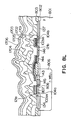
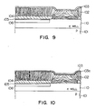
- Figs. 9 and 10 are enlargements of the part enclosed by the box A in Fig. 8.
- A first embodiment of the present invention will now be described with reference to the accompanying drawings. The basic concept of the method of manufacturing a semiconductor device according to the present invention is shown in Fig. 7. The figure shows the situation after a
polysilicon film 102 that has not yet been patterned is formed on the surface of an n-well 110 formed on a p-type semiconductor substrate 101, and an amorphous (non-crystalline)film 103 is formed on thepolysilicon film 102. Any of a wide range of materials can be used for theamorphous film 103, provided it is amorphous. For example, an insulating material such as silicon dioxide (SiO₂) or silicon nitride (Si₃N₄), or a conducting material that is either a refractory metal such as tungsten, titanium, molybdenum, cobalt, or tantalum or a silicide of a refractory metal such as tungsten silicide, titanium silicide, molybdenum silicide, cobalt silicide, or tantalum silicide, could be used. When boron ions are implanted through thefilm 103 made of such an amorphous material, the direction in which the ions move is refracted by theamorphous film 103, as shown by thearrow 105, and they stop within thepolysilicon film 102. Therefore, the phenomenon that occurs in the conventional device (shown by thearrow 2202 in Fig. 6) in which boron ions penetrate the polysilicon film and are implanted into the channel portion below the gate oxide film, is prevented. - Therefore, the first method for adding only boron element into the
polysilicon film 102 to have a high concentration has realized. Using such a method, the polysilicon film having a high hole concentration suitable for gate electrodes. - The following paragraphs describe the method of manufacturing a semiconductor device in which the above-described
film 103 is designed to prevent unwanted penetration of boron ions. - First the n-well 110 is formed in the region of the
semiconductor substrate 101 that is destined to become the p-channel MOS transistor, then afield oxide film 112 and a fieldinversion prevention layer 113 are formed between the regions destined to become separate elements (Fig. 8A).Points gate oxide film 104 in connection with the drain region on the p-channel MOS transistor side and the drain region on the n-channel MOS transistor side, to allow electrical conduction with those regions. A punch-throughcurrent suppression layer 106 and a counter-dose (for fine control)region 105 are formed under the region destined to form the gate electrode of the p-channel MOS transistor, and a punch-throughcurrent suppression layer 108 and a counter-dose (for fine control)region 107 are formed under the region destined to form the gate electrode of the n-channel MOS transistor. The entire surface is then covered with an approximately 1700Å thick film by a method such as low pressure chemical vapor deposition (LPCVD), to form a polysilicon film 111 to which no impurities have yet been added. - Next, the above-described
amorphous film 103 is formed over the entire surface of the polysilicon film (Fig. 8B). The portion of the device that is destined to become a p-type impurity layer, surrounded by the box A in this figure, is shown enlarged in Fig. 9. As described above, an insulating material such as silicon dioxide (SiO₂) or silicon nitride (Si₃N₄) can be used as theamorphous film 103 formed on top of thepolysilicon film 102. A silicon dioxide film could be formed by CVD under conditions of a mixed gas of silane (SiH₄) and oxygen (O₂) at 1 atmosphere and 400°C, or a silicon nitride film could be formed by plasma CVD under conditions of a mixed gas of silane (SiH₄) and ammonia (NH₃) at 300°C. In addition, the film should be cooled rapidly to ensure that crystallization does not occur. The thickness of the amorphous film is preferably 500 to 1000 Å. - One advantage of using a refractory metal such as tungsten, titanium, or molybdenum, or a silicide of a refractory metal such as tungsten silicide, titanium silicide, or molybdenum silicide, as the conductive material is the fact that it can be formed by a CVD or sputtering method to a thickness of, for example, 200 to 1000 Å.
- The
amorphous film 103 can be formed in one of the above-described ways, but if it is too thin, there is the worry that the internal reactions caused by subsequent high-dosage implantation of boron ions will result in peeling of theamorphous film 103. Therefore, if theamorphous film 103 is of a refractory metal, a method such as rapid thermal annealing could be used at this point to turn asurface 103a thereof in contact with thepolysilicon film 102 into the silicide, as shown in Fig. 10, to prevent peeling. - After a resist
film 114 is formed over the entire surface of theamorphous film 103, either wet or dry etching is used to remove unwanted portions thereof, leaving portions thereof over the regions destined to become the n-channel MOS transistor and an n-type impurity region, as shown in Fig. 8C. The resistfilm 114 is then used as a mask for the implantation of boron ions at a dosage of, for example, 5 x 10¹⁶ atoms/cm² with an accelerating voltage of 30 keV through theamorphous film 103 into thepolysilicon film 102 above the regions destined to become the p-channel MOS transistor and a p-type impurity region. This process results in apolysilicon film 102a into which boron ions have been implanted at a high concentration, as shown in Fig. 8D. In this case, since the boron ions are implanted through theamorphous film 103, they stop within the interior of thepolysilicon film 102, and do not penetrate as far as thecounter-dose region 105. - The resist
film 114 is then peeled off by an asher such as an oxygen plasma, then it is completely removed by processing involving a hot mixture of liquids such as sulfuric acid and hydrogen peroxide. Resist is then applied to the entire surface, and it is patterned to form a resistfilm 131 that remains above the regions destined to become the p-channel MOS transistor and the p-type impurity region. The resistfilm 131 is used as a mask for the implantation of phosphorous ions (P⁺) at a dosage of, for example, 5 x 10¹⁶ atoms/cm² with an accelerating voltage of 50 keV through theamorphous film 103 into thepolysilicon film 102 above the region destined to become the n-channel MOS transistor. In this case, since a large number of atoms of phosphorous or arsenic are implanted as the n-type impurity, they pass through theamorphous film 103 but are stopped within thepolysilicon film 102, so they do not penetrate as far as thecounter-dose region 107. - The resist
film 131 and theamorphous film 103 are then removed. If theamorphous film 103 is made of an insulating material such as silicon dioxide, it must be removed at this point; but if it is made of a conductive material such as tungsten or tungsten silicide, there is no need to remove it. The processing so far has formed apolysilicon film 102a into which boron ions (p-type impurity ions) have been implanted above the region destined to become the p-channel MOS transistor, and apolysilicon film 102b into which phosphorous ions (n-type impurity ions) have been implanted above the region destined to become the n-channel MOS transistor (Fig. 8E). - Over the entire surface of the
polysilicon films metal silicide film 121 of a silicide of a refractory metal, such as tungsten silicide, is then formed to a thickness of approximately 2500 Å (Fig. 8F). - At this stage, a suitable heat treatment temperature cycle could be applied in a diffusion furnace or a rapid thermal furnace in order to adjust the film quality of the
metal silicide film 121, but this step is not necessary if its omission would not cause any problems in subsequent steps. The boron and phosphorous impurities are electrically active, so they migrate and disperse from thepolysilicon films conductive layers metal silicide film 121 and thepolysilicon films conductive film 122 of a resistance lower than that of polysilicon is formed from the polysilicon and the metal silicide by the migration and dispersion of boron and phosphorous ions (Fig. 8G). - Another layer of resist is then applied and a resist
film 132 is formed therefrom by photolithography (Fig. 8H). This resistfilm 132 is used as a mask for patterning thegate oxide film 104, thepolysilicon films conductive film 122, by a method such as reactive ion etching (RIE), then the resistfilm 132 is removed by means such as an asher and hot liquid processing (Fig. 8I). This step results in a gate electrode on the p-channel MOS transistor side formed of a multi-layer structure comprising agate oxide film 104a, a polysilicon film 102aa, and ametal silicide film 121a; a gate electrode on the n-channel MOS transistor side formed of a multi-layer structure comprising agate oxide film 104b, a polysilicon film 102bb, and a metal silicide film 121b; and an inverter output electrode formed of agate oxide film 104c, a polysilicon film 102cc, and ametal silicide film 121c, (which contains the conductive film 122). - A resist
film 135 is then used as a mask for the implantation of boron ions to form a p-type impurity layer 134 to act as a source of the p-channel MOS transistor and a p-type impurity layer 145 to act as a drain of the same transistor (Fig. 8J); and a resistfilm 136 is used as a mask for the implantation of phosphorous ions to form an n-type impurity layer 137 to act as a source of the n-channel MOS transistor and an n-type impurity layer 146 to act as a drain of the same transistor (Fig. 8K). - Subsequently, a first layer of wiring 1702 and an
inter-layer isolation film 1701, and a second layer ofwiring 1704 and aninter-layer isolation film 1703 are formed on the surface, then apassivation film 1706 is formed over the entire surface (Fig. 8L). - In the structure formed by the above method, boron ions are prevented by the
amorphous film 103 from penetrating into the channel portion (thecounter-dose region 105 and punch-through current suppression layer 106) below thepolysilicon film 102, so the threshold voltage does not deviate from its initial value set at the design stage, and hence it can be controlled with a high degree of accuracy. - It should be noted that if the
amorphous film 103 of Fig. 8B is made of a refractory metal such as tungsten, instead of a metal silicide, a suitable thermal processing temperature cycle in a heat furnace or a rapid thermal furnace could be employed to control the conversion of the metal into its silicide, optimizing residual stresses and reducing resistance. Theamorphous film 103 could comprise combination of several different materials, not just one, but the use of equipment that can form these materials sequentially or alternately in the same chamber by sputtering is preferable to reduce the time required for the manufacture. The use of an amorphous film formed by the above-described method can provide complementary MOS transistors that have gate electrodes of lower resistances and threshold voltages that are approximately the same as their design values. - The above-described embodiment is nothing but an example of the present invention; it should not be taken as limiting the present invention in any way. For example, an n-type impurity is implanted into the
polysilicon film 102 on the n-channel MOS transistor side in the step shown in Fig. 8D, but this ion implantation could be replaced with batch implantation over the entire surface by a phosphorous trichlorate (POCl₃) doping method, or electrically active impurities could be added during an LPCVD method process when theamorphous film 103 is formed beforehand. In addition, theamorphous film 103 that is formed over the surface of the polysilicon film 111 in the step shown in Fig. 8B could also be formed by implanting arsenic ions into the polysilicon film 111 at a high dosage of, for example 5 x 10¹⁶ atoms/cm² with an accelerating voltage of 30 keV. Since the quantity of arsenic ions is so high, they are implanted at a high concentration, making the surface of the polysilicon film 111 amorphous. As a result, theamorphous film 103 formed over the surface of the polysilicon film 111 will also serve to prevent the penetration of boron ions during the subsequent implantation thereof.
Claims (4)
forming a gate oxide film over the surface of a semiconductor substrate in a region where a p-channel MOS transistor is to be formed;
forming a polysilicon film over said gate oxide film, in order to construct a gate electrode;
forming a film of an amorphous material over said polysilicon film; and
implanting ions of a p-type impurity into said polysilicon film, through said film of amorphous material.
Applications Claiming Priority (2)
| Application Number | Priority Date | Filing Date | Title |
|---|---|---|---|
| JP145641/89 | 1989-06-08 | ||
| JP1145641A JPH0758701B2 (en) | 1989-06-08 | 1989-06-08 | Method for manufacturing semiconductor device |
Publications (3)
| Publication Number | Publication Date |
|---|---|
| EP0402784A2 true EP0402784A2 (en) | 1990-12-19 |
| EP0402784A3 EP0402784A3 (en) | 1990-12-27 |
| EP0402784B1 EP0402784B1 (en) | 1996-12-18 |
Family
ID=15389710
Family Applications (1)
| Application Number | Title | Priority Date | Filing Date |
|---|---|---|---|
| EP90110875A Expired - Lifetime EP0402784B1 (en) | 1989-06-08 | 1990-06-08 | Method of manufacturing a CMOS semiconductor device |
Country Status (5)
| Country | Link |
|---|---|
| US (2) | US5464789A (en) |
| EP (1) | EP0402784B1 (en) |
| JP (1) | JPH0758701B2 (en) |
| KR (1) | KR930009031B1 (en) |
| DE (1) | DE69029430T2 (en) |
Cited By (4)
| Publication number | Priority date | Publication date | Assignee | Title |
|---|---|---|---|---|
| EP0495541A1 (en) * | 1991-01-16 | 1992-07-22 | Koninklijke Philips Electronics N.V. | Method of manufacturing a semiconductor device provided with a field effect transistor |
| EP0637073A1 (en) * | 1993-07-29 | 1995-02-01 | STMicroelectronics S.r.l. | Process for realizing low threshold P-channel MOS transistors for complementary devices (CMOS) |
| EP0643417A3 (en) * | 1993-09-08 | 1995-10-04 | At & T Corp | Method for installing the door. |
| US5652156A (en) * | 1995-04-10 | 1997-07-29 | Taiwan Semiconductor Manufacturing Company Ltd. | Layered polysilicon deposition method |
Families Citing this family (23)
| Publication number | Priority date | Publication date | Assignee | Title |
|---|---|---|---|---|
| JPH0758701B2 (en) * | 1989-06-08 | 1995-06-21 | 株式会社東芝 | Method for manufacturing semiconductor device |
| EP0789401A3 (en) * | 1995-08-25 | 1998-09-16 | Matsushita Electric Industrial Co., Ltd. | LD MOSFET or MOSFET with an integrated circuit containing thereof and manufacturing method |
| KR0149256B1 (en) * | 1995-08-25 | 1998-10-01 | 김주용 | A method for fabricating a cmos transistor |
| US5981364A (en) * | 1995-12-06 | 1999-11-09 | Advanced Micro Devices, Inc. | Method of forming a silicon gate to produce silicon devices with improved performance |
| KR0172788B1 (en) * | 1995-12-29 | 1999-03-30 | 김주용 | Transistor manufacturing method of semiconductor device |
| US6188136B1 (en) * | 1996-06-26 | 2001-02-13 | Kabushiki Kaisha Toshiba | Semiconductor device including a wiring layer having a non-doped or high resistivity polycrystal silicon portion |
| US5882962A (en) * | 1996-07-29 | 1999-03-16 | Vanguard International Semiconductor Corporation | Method of fabricating MOS transistor having a P+ -polysilicon gate |
| US5763923A (en) * | 1996-08-13 | 1998-06-09 | Micron Technology, Inc. | Compound PVD target material for semiconductor metallization |
| US5770490A (en) * | 1996-08-29 | 1998-06-23 | International Business Machines Corporation | Method for producing dual work function CMOS device |
| US6028339A (en) * | 1996-08-29 | 2000-02-22 | International Business Machines Corporation | Dual work function CMOS device |
| US5747368A (en) * | 1996-10-03 | 1998-05-05 | Mosel Vitelic Inc. | Process for manufacturing CMOS device |
| TW342532B (en) * | 1996-10-11 | 1998-10-11 | United Microelectronics Corp | Process for producing dual-gate CMOS component by compensating implantation |
| US6127214A (en) * | 1996-12-09 | 2000-10-03 | Texas Instruments Incorporated | Contact gate structure and method |
| US6406952B2 (en) * | 1997-07-14 | 2002-06-18 | Agere Systems Guardian Corp. | Process for device fabrication |
| US5963799A (en) * | 1998-03-23 | 1999-10-05 | Texas Instruments - Acer Incorporated | Blanket well counter doping process for high speed/low power MOSFETs |
| US6566181B2 (en) | 1999-02-26 | 2003-05-20 | Agere Systems Inc. | Process for the fabrication of dual gate structures for CMOS devices |
| US6492688B1 (en) | 1999-03-02 | 2002-12-10 | Siemens Aktiengesellschaft | Dual work function CMOS device |
| US6344669B1 (en) * | 2000-06-13 | 2002-02-05 | United Microelectronics Corp. | CMOS sensor |
| US6770921B2 (en) * | 2001-08-31 | 2004-08-03 | Micron Technology, Inc. | Sidewall strap for complementary semiconductor structures and method of making same |
| US6867087B2 (en) * | 2001-11-19 | 2005-03-15 | Infineon Technologies Ag | Formation of dual work function gate electrode |
| US20030218218A1 (en) * | 2002-05-21 | 2003-11-27 | Samir Chaudhry | SRAM cell with reduced standby leakage current and method for forming the same |
| US7486541B2 (en) * | 2003-06-13 | 2009-02-03 | Taiwan Semiconductor Manufacturing Company, Ltd. | Resistive cell structure for reducing soft error rate |
| US8252640B1 (en) | 2006-11-02 | 2012-08-28 | Kapre Ravindra M | Polycrystalline silicon activation RTA |
Family Cites Families (39)
| Publication number | Priority date | Publication date | Assignee | Title |
|---|---|---|---|---|
| ZA734354B (en) * | 1972-07-18 | 1974-05-29 | Westinghouse Electric Corp | An improvement in or relating to dielectric fluids and capacitors |
| US3793090A (en) * | 1972-11-21 | 1974-02-19 | Ibm | Method for stabilizing fet devices having silicon gates and composite nitride-oxide gate dielectrics |
| US4222145A (en) * | 1977-11-02 | 1980-09-16 | Clarke-Gravely Corporation | Vacuum cleaner carriage and tank assembly |
| US4374700A (en) * | 1981-05-29 | 1983-02-22 | Texas Instruments Incorporated | Method of manufacturing silicide contacts for CMOS devices |
| IT1213120B (en) * | 1984-01-10 | 1989-12-14 | Ates Componenti Elettron | PROCESS FOR THE MANUFACTURE OF COMPLEMENTARY LOW VOLTAGE THRESHOLD MOS TRANSISTORS IN HIGH DENSITY INTEGRATED CIRCUITS AND RESULTING STRUCTURE. |
| FR2562327B1 (en) * | 1984-03-30 | 1986-06-20 | Commissariat Energie Atomique | METHOD FOR INTERCONNECTING ACTIVE ZONES AND / OR GRIDS OF INTEGRATED CMOS CIRCUITS |
| US4873204A (en) * | 1984-06-15 | 1989-10-10 | Hewlett-Packard Company | Method for making silicide interconnection structures for integrated circuit devices |
| US4584026A (en) * | 1984-07-25 | 1986-04-22 | Rca Corporation | Ion-implantation of phosphorus, arsenic or boron by pre-amorphizing with fluorine ions |
| US4617066A (en) * | 1984-11-26 | 1986-10-14 | Hughes Aircraft Company | Process of making semiconductors having shallow, hyperabrupt doped regions by implantation and two step annealing |
| US5190886A (en) * | 1984-12-11 | 1993-03-02 | Seiko Epson Corporation | Semiconductor device and method of production |
| JPS61139058A (en) * | 1984-12-11 | 1986-06-26 | Seiko Epson Corp | Production apparatus for semiconductor |
| US4821085A (en) * | 1985-05-01 | 1989-04-11 | Texas Instruments Incorporated | VLSI local interconnect structure |
| US5010032A (en) * | 1985-05-01 | 1991-04-23 | Texas Instruments Incorporated | Process for making CMOS device with both P+ and N+ gates including refractory metal silicide and nitride interconnects |
| ES288378Y (en) * | 1985-07-26 | 1986-09-16 | Carbonell Compania Anonima | HYDRAULIC CONNECTION MECHANISM FOR THE INDUSTRIAL WASHING MACHINE DRUM |
| US4782033A (en) * | 1985-11-27 | 1988-11-01 | Siemens Aktiengesellschaft | Process for producing CMOS having doped polysilicon gate by outdiffusion of boron from implanted silicide gate |
| GB2190790B (en) * | 1986-05-12 | 1989-12-13 | Plessey Co Plc | Improvements in transistors |
| US4693324A (en) * | 1986-08-01 | 1987-09-15 | Automation Industries, Inc. | Current-carrying flexible hose |
| JPS6362108A (en) * | 1986-09-02 | 1988-03-18 | 日本電気株式会社 | Flexible circuit |
| JPS63187622A (en) * | 1987-01-30 | 1988-08-03 | Toshiba Corp | Manufacture of semiconductor device |
| US5066995A (en) * | 1987-03-13 | 1991-11-19 | Harris Corporation | Double level conductor structure |
| US4745079A (en) * | 1987-03-30 | 1988-05-17 | Motorola, Inc. | Method for fabricating MOS transistors having gates with different work functions |
| US4728391A (en) * | 1987-05-11 | 1988-03-01 | Motorola Inc. | Pedestal transistors and method of production thereof |
| JPS63299328A (en) * | 1987-05-29 | 1988-12-06 | Matsushita Electric Ind Co Ltd | Impurity introduction |
| US4904611A (en) * | 1987-09-18 | 1990-02-27 | Xerox Corporation | Formation of large grain polycrystalline films |
| NL8800220A (en) * | 1988-01-29 | 1989-08-16 | Philips Nv | METHOD FOR MANUFACTURING A SEMICONDUCTOR DEVICE, IN WHICH A METAL CONDUCTOR TRACK IS APPLIED ON A SURFACE OF A SEMICONDUCTOR BODY. |
| JPH01216572A (en) * | 1988-02-24 | 1989-08-30 | Nec Corp | Manufacture of semiconductor device |
| US5418179A (en) * | 1988-05-31 | 1995-05-23 | Yamaha Corporation | Process of fabricating complementary inverter circuit having multi-level interconnection |
| DE3829211C1 (en) * | 1988-08-29 | 1989-05-18 | Thermo.Form Gmbh, 6453 Seligenstadt, De | Belt fastener |
| US5304502A (en) * | 1988-11-08 | 1994-04-19 | Yamaha Corporation | Process of fabricating semiconductor integrated circuit having conductive strips used as resistor and gate electrode of component transistor |
| JPH02278867A (en) * | 1989-04-20 | 1990-11-15 | Oki Electric Ind Co Ltd | Complementary mos field effect transistor |
| JPH0758701B2 (en) * | 1989-06-08 | 1995-06-21 | 株式会社東芝 | Method for manufacturing semiconductor device |
| JPH0770727B2 (en) * | 1989-06-16 | 1995-07-31 | 日本電装株式会社 | Method for manufacturing MIS transistor and complementary MIS transistor |
| US5154946A (en) * | 1990-09-27 | 1992-10-13 | Motorola, Inc. | CMOS structure fabrication |
| US5124280A (en) * | 1991-01-31 | 1992-06-23 | Sgs-Thomson Microelectronics, Inc. | Local interconnect for integrated circuits |
| US5190893A (en) * | 1991-04-01 | 1993-03-02 | Motorola Inc. | Process for fabricating a local interconnect structure in a semiconductor device |
| US5298782A (en) * | 1991-06-03 | 1994-03-29 | Sgs-Thomson Microelectronics, Inc. | Stacked CMOS SRAM cell with polysilicon transistor load |
| DE4121051A1 (en) * | 1991-06-26 | 1993-01-07 | Eurosil Electronic Gmbh | SEMICONDUCTOR ARRANGEMENT AND PRODUCTION METHOD |
| JPH05243178A (en) * | 1991-10-03 | 1993-09-21 | Hewlett Packard Co <Hp> | Method for forming connector for semiconductor integrated circuit |
| US5134085A (en) * | 1991-11-21 | 1992-07-28 | Micron Technology, Inc. | Reduced-mask, split-polysilicon CMOS process, incorporating stacked-capacitor cells, for fabricating multi-megabit dynamic random access memories |
-
1989
- 1989-06-08 JP JP1145641A patent/JPH0758701B2/en not_active Expired - Fee Related
-
1990
- 1990-05-31 KR KR1019900007992A patent/KR930009031B1/en not_active Expired - Fee Related
- 1990-06-08 EP EP90110875A patent/EP0402784B1/en not_active Expired - Lifetime
- 1990-06-08 DE DE69029430T patent/DE69029430T2/en not_active Expired - Fee Related
-
1993
- 1993-07-23 US US08/095,995 patent/US5464789A/en not_active Expired - Lifetime
-
1995
- 1995-05-03 US US08/434,406 patent/US5612245A/en not_active Expired - Fee Related
Cited By (6)
| Publication number | Priority date | Publication date | Assignee | Title |
|---|---|---|---|---|
| EP0495541A1 (en) * | 1991-01-16 | 1992-07-22 | Koninklijke Philips Electronics N.V. | Method of manufacturing a semiconductor device provided with a field effect transistor |
| EP0637073A1 (en) * | 1993-07-29 | 1995-02-01 | STMicroelectronics S.r.l. | Process for realizing low threshold P-channel MOS transistors for complementary devices (CMOS) |
| US5534448A (en) * | 1993-07-29 | 1996-07-09 | Sgs-Thomson Microelectronics S.R.L. | Process for realizing P-channel MOS transistors having a low threshold voltage in semiconductor integrated circuits for analog applications |
| US5589701A (en) * | 1993-07-29 | 1996-12-31 | Sgs-Thomson Microelectronics S.R.1. | Process for realizing P-channel MOS transistors having a low threshold voltage in semiconductor integrated circuits for analog applications |
| EP0643417A3 (en) * | 1993-09-08 | 1995-10-04 | At & T Corp | Method for installing the door. |
| US5652156A (en) * | 1995-04-10 | 1997-07-29 | Taiwan Semiconductor Manufacturing Company Ltd. | Layered polysilicon deposition method |
Also Published As
| Publication number | Publication date |
|---|---|
| EP0402784A3 (en) | 1990-12-27 |
| JPH0311627A (en) | 1991-01-18 |
| DE69029430T2 (en) | 1997-05-15 |
| US5464789A (en) | 1995-11-07 |
| DE69029430D1 (en) | 1997-01-30 |
| KR910001993A (en) | 1991-01-31 |
| KR930009031B1 (en) | 1993-09-18 |
| JPH0758701B2 (en) | 1995-06-21 |
| US5612245A (en) | 1997-03-18 |
| EP0402784B1 (en) | 1996-12-18 |
Similar Documents
| Publication | Publication Date | Title |
|---|---|---|
| US5464789A (en) | Method of manufacturing a CMOS semiconductor device | |
| EP0388000B1 (en) | Process for forming vertical bipolar transistors and high-voltage CMOS in a single integrated circuit chip | |
| KR900008207B1 (en) | Semiconductor memory device | |
| US6083780A (en) | Semiconductor device and method of fabrication thereof | |
| US5620922A (en) | Method for fabricating CMOS device having low and high resistance portions and wire formed from a single gate polysilicon | |
| US5294822A (en) | Polycide local interconnect method and structure | |
| US4663825A (en) | Method of manufacturing semiconductor device | |
| US5726459A (en) | GE-SI SOI MOS transistor and method of fabricating same | |
| US5432129A (en) | Method of forming low resistance contacts at the junction between regions having different conductivity types | |
| US5744845A (en) | Complementary MOS field effect transistor with tunnel effect means | |
| US5026654A (en) | Method of manufacturing a semiconductor device utilizing a single polycrystalline layer for all electrodes | |
| EP0051500B1 (en) | Semiconductor devices | |
| US6214681B1 (en) | Process for forming polysilicon/germanium thin films without germanium outgassing | |
| US6020260A (en) | Method of fabricating a semiconductor device having nitrogen-bearing gate electrode | |
| KR100324144B1 (en) | Semiconductor Device and Method for Making the Same | |
| US6127216A (en) | Heavily-doped polysilicon/germanium thin film formed by laser annealing | |
| US5153146A (en) | Maufacturing method of semiconductor devices | |
| KR100391891B1 (en) | Manufacturing Method of Semiconductor Device | |
| KR100202048B1 (en) | Process for fabricating power-mos semiconductor device and device obtained therewith | |
| US5116770A (en) | Method for fabricating bipolar semiconductor devices | |
| US5612243A (en) | Polycide local interconnect method and structure | |
| US5882962A (en) | Method of fabricating MOS transistor having a P+ -polysilicon gate | |
| US5146309A (en) | Method for forming polycrystalline silicon contacts | |
| US5236851A (en) | Method for fabricating semiconductor devices | |
| JPH05291180A (en) | Manufacture of semiconductor integrated |
Legal Events
| Date | Code | Title | Description |
|---|---|---|---|
| PUAI | Public reference made under article 153(3) epc to a published international application that has entered the european phase |
Free format text: ORIGINAL CODE: 0009012 |
|
| PUAL | Search report despatched |
Free format text: ORIGINAL CODE: 0009013 |
|
| 17P | Request for examination filed |
Effective date: 19900608 |
|
| AK | Designated contracting states |
Kind code of ref document: A2 Designated state(s): DE FR GB |
|
| 17Q | First examination report despatched |
Effective date: 19930909 |
|
| GRAG | Despatch of communication of intention to grant |
Free format text: ORIGINAL CODE: EPIDOS AGRA |
|
| GRAH | Despatch of communication of intention to grant a patent |
Free format text: ORIGINAL CODE: EPIDOS IGRA |
|
| RAP1 | Party data changed (applicant data changed or rights of an application transferred) |
Owner name: KABUSHIKI KAISHA TOSHIBA |
|
| GRAH | Despatch of communication of intention to grant a patent |
Free format text: ORIGINAL CODE: EPIDOS IGRA |
|
| GRAA | (expected) grant |
Free format text: ORIGINAL CODE: 0009210 |
|
| AK | Designated contracting states |
Kind code of ref document: B1 Designated state(s): DE FR GB |
|
| REF | Corresponds to: |
Ref document number: 69029430 Country of ref document: DE Date of ref document: 19970130 |
|
| ET | Fr: translation filed | ||
| PLBE | No opposition filed within time limit |
Free format text: ORIGINAL CODE: 0009261 |
|
| STAA | Information on the status of an ep patent application or granted ep patent |
Free format text: STATUS: NO OPPOSITION FILED WITHIN TIME LIMIT |
|
| 26N | No opposition filed | ||
| REG | Reference to a national code |
Ref country code: GB Ref legal event code: 746 Effective date: 19981010 |
|
| REG | Reference to a national code |
Ref country code: FR Ref legal event code: D6 |
|
| REG | Reference to a national code |
Ref country code: GB Ref legal event code: IF02 |
|
| PGFP | Annual fee paid to national office [announced via postgrant information from national office to epo] |
Ref country code: DE Payment date: 20070531 Year of fee payment: 18 |
|
| PGFP | Annual fee paid to national office [announced via postgrant information from national office to epo] |
Ref country code: GB Payment date: 20070606 Year of fee payment: 18 |
|
| PGFP | Annual fee paid to national office [announced via postgrant information from national office to epo] |
Ref country code: FR Payment date: 20070608 Year of fee payment: 18 |
|
| GBPC | Gb: european patent ceased through non-payment of renewal fee |
Effective date: 20080608 |
|
| REG | Reference to a national code |
Ref country code: FR Ref legal event code: ST Effective date: 20090228 |
|
| PG25 | Lapsed in a contracting state [announced via postgrant information from national office to epo] |
Ref country code: DE Free format text: LAPSE BECAUSE OF NON-PAYMENT OF DUE FEES Effective date: 20090101 |
|
| PG25 | Lapsed in a contracting state [announced via postgrant information from national office to epo] |
Ref country code: GB Free format text: LAPSE BECAUSE OF NON-PAYMENT OF DUE FEES Effective date: 20080608 |
|
| PG25 | Lapsed in a contracting state [announced via postgrant information from national office to epo] |
Ref country code: FR Free format text: LAPSE BECAUSE OF NON-PAYMENT OF DUE FEES Effective date: 20080630 |