EP0401983B1 - Thin film device for rotational magnetic flux conduction - Google Patents
Thin film device for rotational magnetic flux conduction Download PDFInfo
- Publication number
- EP0401983B1 EP0401983B1 EP90305150A EP90305150A EP0401983B1 EP 0401983 B1 EP0401983 B1 EP 0401983B1 EP 90305150 A EP90305150 A EP 90305150A EP 90305150 A EP90305150 A EP 90305150A EP 0401983 B1 EP0401983 B1 EP 0401983B1
- Authority
- EP
- European Patent Office
- Prior art keywords
- layers
- flux
- magnetic
- domains
- magnetic domains
- Prior art date
- Legal status (The legal status is an assumption and is not a legal conclusion. Google has not performed a legal analysis and makes no representation as to the accuracy of the status listed.)
- Expired - Lifetime
Links
- 230000004907 flux Effects 0.000 title claims abstract description 152
- 230000005291 magnetic effect Effects 0.000 title claims abstract description 70
- 239000010409 thin film Substances 0.000 title claims abstract description 20
- 238000000034 method Methods 0.000 claims abstract description 25
- 230000005381 magnetic domain Effects 0.000 claims description 47
- 230000008878 coupling Effects 0.000 claims description 9
- 238000010168 coupling process Methods 0.000 claims description 9
- 238000005859 coupling reaction Methods 0.000 claims description 9
- 230000008021 deposition Effects 0.000 claims description 4
- 230000007480 spreading Effects 0.000 abstract description 14
- 238000003892 spreading Methods 0.000 abstract description 14
- 238000004519 manufacturing process Methods 0.000 abstract description 4
- 230000005415 magnetization Effects 0.000 description 9
- 230000007246 mechanism Effects 0.000 description 9
- 230000008569 process Effects 0.000 description 8
- 239000010408 film Substances 0.000 description 7
- 238000006073 displacement reaction Methods 0.000 description 5
- 238000000151 deposition Methods 0.000 description 4
- 230000000295 complement effect Effects 0.000 description 3
- 238000000469 dry deposition Methods 0.000 description 3
- 230000000694 effects Effects 0.000 description 3
- 239000000463 material Substances 0.000 description 3
- 230000003068 static effect Effects 0.000 description 3
- 230000005330 Barkhausen effect Effects 0.000 description 2
- XEEYBQQBJWHFJM-UHFFFAOYSA-N Iron Chemical compound [Fe] XEEYBQQBJWHFJM-UHFFFAOYSA-N 0.000 description 2
- 238000013459 approach Methods 0.000 description 2
- 230000008901 benefit Effects 0.000 description 2
- 230000015572 biosynthetic process Effects 0.000 description 2
- 239000000919 ceramic Substances 0.000 description 2
- 239000013078 crystal Substances 0.000 description 2
- 230000007547 defect Effects 0.000 description 2
- 238000013461 design Methods 0.000 description 2
- 230000006698 induction Effects 0.000 description 2
- 239000002184 metal Substances 0.000 description 2
- 229910052751 metal Inorganic materials 0.000 description 2
- 238000012545 processing Methods 0.000 description 2
- 230000000644 propagated effect Effects 0.000 description 2
- 229910000531 Co alloy Inorganic materials 0.000 description 1
- 229910000640 Fe alloy Inorganic materials 0.000 description 1
- 229910001030 Iron–nickel alloy Inorganic materials 0.000 description 1
- 229910000990 Ni alloy Inorganic materials 0.000 description 1
- 229910018104 Ni-P Inorganic materials 0.000 description 1
- 229910018536 Ni—P Inorganic materials 0.000 description 1
- 230000009286 beneficial effect Effects 0.000 description 1
- 230000005540 biological transmission Effects 0.000 description 1
- 230000008859 change Effects 0.000 description 1
- 238000006243 chemical reaction Methods 0.000 description 1
- 239000010941 cobalt Substances 0.000 description 1
- GUTLYIVDDKVIGB-UHFFFAOYSA-N cobalt atom Chemical compound [Co] GUTLYIVDDKVIGB-UHFFFAOYSA-N 0.000 description 1
- 229910052802 copper Inorganic materials 0.000 description 1
- 230000003292 diminished effect Effects 0.000 description 1
- 238000005516 engineering process Methods 0.000 description 1
- 230000007717 exclusion Effects 0.000 description 1
- 230000005294 ferromagnetic effect Effects 0.000 description 1
- 239000002223 garnet Substances 0.000 description 1
- 229910052737 gold Inorganic materials 0.000 description 1
- 238000010438 heat treatment Methods 0.000 description 1
- 230000001939 inductive effect Effects 0.000 description 1
- 230000003993 interaction Effects 0.000 description 1
- 238000010030 laminating Methods 0.000 description 1
- 238000003475 lamination Methods 0.000 description 1
- 239000000203 mixture Substances 0.000 description 1
- 230000035699 permeability Effects 0.000 description 1
- 238000007747 plating Methods 0.000 description 1
- 230000001902 propagating effect Effects 0.000 description 1
- 230000009467 reduction Effects 0.000 description 1
- 230000004044 response Effects 0.000 description 1
- 230000035945 sensitivity Effects 0.000 description 1
- 238000004544 sputter deposition Methods 0.000 description 1
- 238000000992 sputter etching Methods 0.000 description 1
- 239000000758 substrate Substances 0.000 description 1
- 238000012546 transfer Methods 0.000 description 1
- 238000001771 vacuum deposition Methods 0.000 description 1
- 229910000859 α-Fe Inorganic materials 0.000 description 1
Images




Classifications
-
- G—PHYSICS
- G01—MEASURING; TESTING
- G01R—MEASURING ELECTRIC VARIABLES; MEASURING MAGNETIC VARIABLES
- G01R33/00—Arrangements or instruments for measuring magnetic variables
- G01R33/02—Measuring direction or magnitude of magnetic fields or magnetic flux
-
- B—PERFORMING OPERATIONS; TRANSPORTING
- B82—NANOTECHNOLOGY
- B82Y—SPECIFIC USES OR APPLICATIONS OF NANOSTRUCTURES; MEASUREMENT OR ANALYSIS OF NANOSTRUCTURES; MANUFACTURE OR TREATMENT OF NANOSTRUCTURES
- B82Y25/00—Nanomagnetism, e.g. magnetoimpedance, anisotropic magnetoresistance, giant magnetoresistance or tunneling magnetoresistance
-
- B—PERFORMING OPERATIONS; TRANSPORTING
- B82—NANOTECHNOLOGY
- B82Y—SPECIFIC USES OR APPLICATIONS OF NANOSTRUCTURES; MEASUREMENT OR ANALYSIS OF NANOSTRUCTURES; MANUFACTURE OR TREATMENT OF NANOSTRUCTURES
- B82Y40/00—Manufacture or treatment of nanostructures
-
- G—PHYSICS
- G11—INFORMATION STORAGE
- G11B—INFORMATION STORAGE BASED ON RELATIVE MOVEMENT BETWEEN RECORD CARRIER AND TRANSDUCER
- G11B5/00—Recording by magnetisation or demagnetisation of a record carrier; Reproducing by magnetic means; Record carriers therefor
- G11B5/127—Structure or manufacture of heads, e.g. inductive
- G11B5/31—Structure or manufacture of heads, e.g. inductive using thin films
- G11B5/3109—Details
- G11B5/3113—Details for improving the magnetic domain structure or avoiding the formation or displacement of undesirable magnetic domains
-
- G—PHYSICS
- G11—INFORMATION STORAGE
- G11B—INFORMATION STORAGE BASED ON RELATIVE MOVEMENT BETWEEN RECORD CARRIER AND TRANSDUCER
- G11B5/00—Recording by magnetisation or demagnetisation of a record carrier; Reproducing by magnetic means; Record carriers therefor
- G11B5/127—Structure or manufacture of heads, e.g. inductive
- G11B5/31—Structure or manufacture of heads, e.g. inductive using thin films
- G11B5/3109—Details
- G11B5/313—Disposition of layers
- G11B5/3143—Disposition of layers including additional layers for improving the electromagnetic transducing properties of the basic structure, e.g. for flux coupling, guiding or shielding
-
- G—PHYSICS
- G11—INFORMATION STORAGE
- G11B—INFORMATION STORAGE BASED ON RELATIVE MOVEMENT BETWEEN RECORD CARRIER AND TRANSDUCER
- G11B5/00—Recording by magnetisation or demagnetisation of a record carrier; Reproducing by magnetic means; Record carriers therefor
- G11B5/127—Structure or manufacture of heads, e.g. inductive
- G11B5/31—Structure or manufacture of heads, e.g. inductive using thin films
- G11B5/3109—Details
- G11B5/313—Disposition of layers
- G11B5/3143—Disposition of layers including additional layers for improving the electromagnetic transducing properties of the basic structure, e.g. for flux coupling, guiding or shielding
- G11B5/3146—Disposition of layers including additional layers for improving the electromagnetic transducing properties of the basic structure, e.g. for flux coupling, guiding or shielding magnetic layers
- G11B5/3153—Disposition of layers including additional layers for improving the electromagnetic transducing properties of the basic structure, e.g. for flux coupling, guiding or shielding magnetic layers including at least one magnetic thin film coupled by interfacing to the basic magnetic thin film structure
-
- G—PHYSICS
- G11—INFORMATION STORAGE
- G11B—INFORMATION STORAGE BASED ON RELATIVE MOVEMENT BETWEEN RECORD CARRIER AND TRANSDUCER
- G11B5/00—Recording by magnetisation or demagnetisation of a record carrier; Reproducing by magnetic means; Record carriers therefor
- G11B5/127—Structure or manufacture of heads, e.g. inductive
- G11B5/31—Structure or manufacture of heads, e.g. inductive using thin films
- G11B5/3109—Details
- G11B5/313—Disposition of layers
- G11B5/3143—Disposition of layers including additional layers for improving the electromagnetic transducing properties of the basic structure, e.g. for flux coupling, guiding or shielding
- G11B5/3146—Disposition of layers including additional layers for improving the electromagnetic transducing properties of the basic structure, e.g. for flux coupling, guiding or shielding magnetic layers
- G11B5/3153—Disposition of layers including additional layers for improving the electromagnetic transducing properties of the basic structure, e.g. for flux coupling, guiding or shielding magnetic layers including at least one magnetic thin film coupled by interfacing to the basic magnetic thin film structure
- G11B5/3156—Disposition of layers including additional layers for improving the electromagnetic transducing properties of the basic structure, e.g. for flux coupling, guiding or shielding magnetic layers including at least one magnetic thin film coupled by interfacing to the basic magnetic thin film structure providing interaction by induced or exchange coupling
-
- G—PHYSICS
- G11—INFORMATION STORAGE
- G11B—INFORMATION STORAGE BASED ON RELATIVE MOVEMENT BETWEEN RECORD CARRIER AND TRANSDUCER
- G11B5/00—Recording by magnetisation or demagnetisation of a record carrier; Reproducing by magnetic means; Record carriers therefor
- G11B5/127—Structure or manufacture of heads, e.g. inductive
- G11B5/31—Structure or manufacture of heads, e.g. inductive using thin films
- G11B5/3176—Structure of heads comprising at least in the transducing gap regions two magnetic thin films disposed respectively at both sides of the gaps
- G11B5/3179—Structure of heads comprising at least in the transducing gap regions two magnetic thin films disposed respectively at both sides of the gaps the films being mainly disposed in parallel planes
-
- G—PHYSICS
- G11—INFORMATION STORAGE
- G11B—INFORMATION STORAGE BASED ON RELATIVE MOVEMENT BETWEEN RECORD CARRIER AND TRANSDUCER
- G11B5/00—Recording by magnetisation or demagnetisation of a record carrier; Reproducing by magnetic means; Record carriers therefor
- G11B5/127—Structure or manufacture of heads, e.g. inductive
- G11B5/33—Structure or manufacture of flux-sensitive heads, i.e. for reproduction only; Combination of such heads with means for recording or erasing only
- G11B5/332—Structure or manufacture of flux-sensitive heads, i.e. for reproduction only; Combination of such heads with means for recording or erasing only using thin films
-
- G—PHYSICS
- G11—INFORMATION STORAGE
- G11B—INFORMATION STORAGE BASED ON RELATIVE MOVEMENT BETWEEN RECORD CARRIER AND TRANSDUCER
- G11B5/00—Recording by magnetisation or demagnetisation of a record carrier; Reproducing by magnetic means; Record carriers therefor
- G11B5/62—Record carriers characterised by the selection of the material
- G11B5/64—Record carriers characterised by the selection of the material comprising only the magnetic material without bonding agent
- G11B5/66—Record carriers characterised by the selection of the material comprising only the magnetic material without bonding agent the record carriers consisting of several layers
- G11B5/674—Record carriers characterised by the selection of the material comprising only the magnetic material without bonding agent the record carriers consisting of several layers having differing macroscopic or microscopic structures, e.g. differing crystalline lattices, varying atomic structures or differing roughnesses
-
- G—PHYSICS
- G11—INFORMATION STORAGE
- G11C—STATIC STORES
- G11C11/00—Digital stores characterised by the use of particular electric or magnetic storage elements; Storage elements therefor
- G11C11/02—Digital stores characterised by the use of particular electric or magnetic storage elements; Storage elements therefor using magnetic elements
- G11C11/14—Digital stores characterised by the use of particular electric or magnetic storage elements; Storage elements therefor using magnetic elements using thin-film elements
-
- G—PHYSICS
- G11—INFORMATION STORAGE
- G11C—STATIC STORES
- G11C11/00—Digital stores characterised by the use of particular electric or magnetic storage elements; Storage elements therefor
- G11C11/02—Digital stores characterised by the use of particular electric or magnetic storage elements; Storage elements therefor using magnetic elements
- G11C11/14—Digital stores characterised by the use of particular electric or magnetic storage elements; Storage elements therefor using magnetic elements using thin-film elements
- G11C11/15—Digital stores characterised by the use of particular electric or magnetic storage elements; Storage elements therefor using magnetic elements using thin-film elements using multiple magnetic layers
-
- H—ELECTRICITY
- H01—ELECTRIC ELEMENTS
- H01F—MAGNETS; INDUCTANCES; TRANSFORMERS; SELECTION OF MATERIALS FOR THEIR MAGNETIC PROPERTIES
- H01F10/00—Thin magnetic films, e.g. of one-domain structure
- H01F10/26—Thin magnetic films, e.g. of one-domain structure characterised by the substrate or intermediate layers
- H01F10/30—Thin magnetic films, e.g. of one-domain structure characterised by the substrate or intermediate layers characterised by the composition of the intermediate layers, e.g. seed, buffer, template, diffusion preventing, cap layers
-
- H—ELECTRICITY
- H01—ELECTRIC ELEMENTS
- H01F—MAGNETS; INDUCTANCES; TRANSFORMERS; SELECTION OF MATERIALS FOR THEIR MAGNETIC PROPERTIES
- H01F10/00—Thin magnetic films, e.g. of one-domain structure
- H01F10/32—Spin-exchange-coupled multilayers, e.g. nanostructured superlattices
-
- H—ELECTRICITY
- H01—ELECTRIC ELEMENTS
- H01F—MAGNETS; INDUCTANCES; TRANSFORMERS; SELECTION OF MATERIALS FOR THEIR MAGNETIC PROPERTIES
- H01F27/00—Details of transformers or inductances, in general
- H01F27/24—Magnetic cores
-
- H—ELECTRICITY
- H01—ELECTRIC ELEMENTS
- H01F—MAGNETS; INDUCTANCES; TRANSFORMERS; SELECTION OF MATERIALS FOR THEIR MAGNETIC PROPERTIES
- H01F27/00—Details of transformers or inductances, in general
- H01F27/34—Special means for preventing or reducing unwanted electric or magnetic effects, e.g. no-load losses, reactive currents, harmonics, oscillations, leakage fields
- H01F27/36—Electric or magnetic shields or screens
-
- H—ELECTRICITY
- H01—ELECTRIC ELEMENTS
- H01F—MAGNETS; INDUCTANCES; TRANSFORMERS; SELECTION OF MATERIALS FOR THEIR MAGNETIC PROPERTIES
- H01F27/00—Details of transformers or inductances, in general
- H01F27/34—Special means for preventing or reducing unwanted electric or magnetic effects, e.g. no-load losses, reactive currents, harmonics, oscillations, leakage fields
- H01F27/36—Electric or magnetic shields or screens
- H01F27/366—Electric or magnetic shields or screens made of ferromagnetic material
-
- H—ELECTRICITY
- H01—ELECTRIC ELEMENTS
- H01F—MAGNETS; INDUCTANCES; TRANSFORMERS; SELECTION OF MATERIALS FOR THEIR MAGNETIC PROPERTIES
- H01F41/00—Apparatus or processes specially adapted for manufacturing or assembling magnets, inductances or transformers; Apparatus or processes specially adapted for manufacturing materials characterised by their magnetic properties
- H01F41/14—Apparatus or processes specially adapted for manufacturing or assembling magnets, inductances or transformers; Apparatus or processes specially adapted for manufacturing materials characterised by their magnetic properties for applying magnetic films to substrates
- H01F41/30—Apparatus or processes specially adapted for manufacturing or assembling magnets, inductances or transformers; Apparatus or processes specially adapted for manufacturing materials characterised by their magnetic properties for applying magnetic films to substrates for applying nanostructures, e.g. by molecular beam epitaxy [MBE]
- H01F41/302—Apparatus or processes specially adapted for manufacturing or assembling magnets, inductances or transformers; Apparatus or processes specially adapted for manufacturing materials characterised by their magnetic properties for applying magnetic films to substrates for applying nanostructures, e.g. by molecular beam epitaxy [MBE] for applying spin-exchange-coupled multilayers, e.g. nanostructured superlattices
-
- Y—GENERAL TAGGING OF NEW TECHNOLOGICAL DEVELOPMENTS; GENERAL TAGGING OF CROSS-SECTIONAL TECHNOLOGIES SPANNING OVER SEVERAL SECTIONS OF THE IPC; TECHNICAL SUBJECTS COVERED BY FORMER USPC CROSS-REFERENCE ART COLLECTIONS [XRACs] AND DIGESTS
- Y10—TECHNICAL SUBJECTS COVERED BY FORMER USPC
- Y10S—TECHNICAL SUBJECTS COVERED BY FORMER USPC CROSS-REFERENCE ART COLLECTIONS [XRACs] AND DIGESTS
- Y10S428/00—Stock material or miscellaneous articles
- Y10S428/90—Magnetic feature
-
- Y—GENERAL TAGGING OF NEW TECHNOLOGICAL DEVELOPMENTS; GENERAL TAGGING OF CROSS-SECTIONAL TECHNOLOGIES SPANNING OVER SEVERAL SECTIONS OF THE IPC; TECHNICAL SUBJECTS COVERED BY FORMER USPC CROSS-REFERENCE ART COLLECTIONS [XRACs] AND DIGESTS
- Y10—TECHNICAL SUBJECTS COVERED BY FORMER USPC
- Y10S—TECHNICAL SUBJECTS COVERED BY FORMER USPC CROSS-REFERENCE ART COLLECTIONS [XRACs] AND DIGESTS
- Y10S428/00—Stock material or miscellaneous articles
- Y10S428/922—Static electricity metal bleed-off metallic stock
- Y10S428/9265—Special properties
- Y10S428/928—Magnetic property
-
- Y—GENERAL TAGGING OF NEW TECHNOLOGICAL DEVELOPMENTS; GENERAL TAGGING OF CROSS-SECTIONAL TECHNOLOGIES SPANNING OVER SEVERAL SECTIONS OF THE IPC; TECHNICAL SUBJECTS COVERED BY FORMER USPC CROSS-REFERENCE ART COLLECTIONS [XRACs] AND DIGESTS
- Y10—TECHNICAL SUBJECTS COVERED BY FORMER USPC
- Y10T—TECHNICAL SUBJECTS COVERED BY FORMER US CLASSIFICATION
- Y10T428/00—Stock material or miscellaneous articles
- Y10T428/11—Magnetic recording head
- Y10T428/1171—Magnetic recording head with defined laminate structural detail
- Y10T428/1186—Magnetic recording head with defined laminate structural detail with head pole component
-
- Y—GENERAL TAGGING OF NEW TECHNOLOGICAL DEVELOPMENTS; GENERAL TAGGING OF CROSS-SECTIONAL TECHNOLOGIES SPANNING OVER SEVERAL SECTIONS OF THE IPC; TECHNICAL SUBJECTS COVERED BY FORMER USPC CROSS-REFERENCE ART COLLECTIONS [XRACs] AND DIGESTS
- Y10—TECHNICAL SUBJECTS COVERED BY FORMER USPC
- Y10T—TECHNICAL SUBJECTS COVERED BY FORMER US CLASSIFICATION
- Y10T428/00—Stock material or miscellaneous articles
- Y10T428/26—Web or sheet containing structurally defined element or component, the element or component having a specified physical dimension
- Y10T428/263—Coating layer not in excess of 5 mils thick or equivalent
- Y10T428/264—Up to 3 mils
- Y10T428/265—1 mil or less
-
- Y—GENERAL TAGGING OF NEW TECHNOLOGICAL DEVELOPMENTS; GENERAL TAGGING OF CROSS-SECTIONAL TECHNOLOGIES SPANNING OVER SEVERAL SECTIONS OF THE IPC; TECHNICAL SUBJECTS COVERED BY FORMER USPC CROSS-REFERENCE ART COLLECTIONS [XRACs] AND DIGESTS
- Y10—TECHNICAL SUBJECTS COVERED BY FORMER USPC
- Y10T—TECHNICAL SUBJECTS COVERED BY FORMER US CLASSIFICATION
- Y10T428/00—Stock material or miscellaneous articles
- Y10T428/31504—Composite [nonstructural laminate]
- Y10T428/31678—Of metal
Definitions
- the present invention relates to rotational flux conduction in thin film magnetic devices.
- Magnetic devices such as thin film recording heads, whether read, read/write, or write, are designed to have particular magnetic orientations, or domains, within the active regions of the device material.
- the static state of each of these domains can be oriented along a given axis, known as the easy axis (or axis of anisotropy), as desired, by control of the manufacturing process.
- Performance is critically linked to domain formation, and, therefore, control can be exerted over device performance by controlling domain formation.
- Domain wall motion results in flux being transmitted through a thin film head along the walls of a domain, or domains, the flux spreading out along the domain walls as the flux seeks to return to equilibrium.
- domain wall motion facilitates conduction of flux at low frequencies, it is a poor vehicle for conduction of flux at high frequencies.
- defects in the material in a magnetic head can be the source of Barkhausen noise during conduction of flux by wall motion as the flux is perturbed by these defects. Such noise can result in erroneous readings of recorded data.
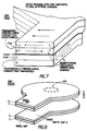
- FIG. 1(a) A conventional prior art pole of a magnetic recording head is shown in Fig. 1(a), where medium M will be seen as inserting signal flux into a first transversely oriented domain d1 of a series of transversely oriented domains d1-dn.
- the rest state flux of the domains is in the X-axis (transverse direction), which leaves a rotational option of flowing into the Y axis (longitudinal direction) or Z axis (vertical direction) in reaction to the signal flux from the medium.
- the Z-axis is out of plane and is a high reluctance path. Hence the flux will rotate into the Y-axis, as indicated by the rotated arrows of each of domains d1-dn.
- conduction of flux by domain-rotation may be achieved by configuring a series of neighboring transverse domains axially aligned along parallel axes, where signal flux impinged upon the first domain at a given angle will cause the magnetization of that domain to rotate from its static orientation by that angle radially into and impinging upon the neighboring domain.
- Such rotation can be transmitted in a like manner along an axis of flux transmission by each neighboring domain of the series.
- flux can be conducted in the pole and through the yoke of a thin film head in a series of domain rotations.
- the yoke enables conduction of flux through a transducer which produces electrical signals proportional to flux levels or the rate of flux change.
- the transducer might be an induction coil or other flux sensing device.
- An induction coil is shown schematically in Fig. 1(a) as it might overlie the bottom pole of a two pole structure.
- a thin film magnetic device capable of conducting signal flux along a first axis, having at least two active magnetic layers for at least one pole, a first of the active magnetic layers having domains which are oriented in a first direction at rest, and a second of the active magnetic layers having domains which are oriented in a second direction at rest.
- the layers are coupled to each other such that the signal flux can flow therebetween.
- WO 89/05505 there is described a laminated pole, for a recording head, comprising two ferromagnetic layers having different uniaxial anisotropies and a non-magnetic layer disposed therebetween.
- the non-magnetic layer exhibits exchange coupling between the magnetic layers so as to eliminate edge domains.
- One aspect of the present invention relates to a method and apparatus for providing rotational flux spreading into the transverse in-plane direction in a flux conduction structure with a preferred rest state not purely in the transverse in-plane direction.
- One feature of the invention is to enable rotational flux spreading in the yoke of a magnetic device.
- a magnetic device has an axis of preferred rest state not purely in the transverse in-plane direction, such that flux spreading into the transverse in-plane direction can occur by rotation.
- a magnetic conduction device has two active layers one at least capable of [both] longitudinal and the other at least capable of lateral flux conduction by rotation. These layers are sufficiently isolated from each other at rest such that the domain state of one layer is independent of the other. However, the layers are sufficiently coupled to each other such that signal flux can readily flow therebetween.
- the layers may have the same width each with different domain orientation or different widths with the same orientations.
- One layer may include a series of strips to form narrow strips of domains.
- the gap between the two layers is small enough to pass rest state domain flux.
- the preferred orientation of the two layers is mainly transverse but is canted at angles of +/- theta relative to the transverse direction. This canting may be by composition or outside bias source. The coupling of the signal flux between these two layers allows the flux to spread in a wedge with an opening angle of about twice theta for small signal levels.
- four active magnetic layers comprise two pairs of layers (AB and CD).
- the layers A and B are oriented in the same direction and the gap between A and B is small enough to couple rest state domain flux between them.
- the layers C and D are similarly configured but their orientation is at a different angle.
- the gap from B to C is large enough to not conduct rest state domain flux but small enough to conduct signal flux.
- a and B could be longitudinally oriented while C and D are transversely oriented.
- a and B could be oriented at plus theta to the transverse direction while C and D are at minus theta.
- a and B are paired as described above and are transversely oriented.
- the gap from B to C is large enough to block rest state domain flux but small enough to conduct signal flux.
- Layer C is oriented longitudinally.
- the pair A and B conducts flux longitudinally even for narrow track widths.
- the layer C spreads the flux laterally thus to avoid the high impedance flux beam effect.
- a and B would be oriented longitudinally and C could be oriented transversely.
- Fig. 1(a) is a schematic view of the top layer of a prior art pole
- Fig. 1(b) is a cross-sectional view of a two layer configuration of the prior art pole of Fig. 1(a).
- Fig. 2 is a schematic of a two layer pole of a preferred embodiment of the present invention.
- Fig. 3 is a schematic of the top layer of the pole of Fig. 2.
- Fig. 4 is a schematic of the bottom layer of the pole of Fig. 2.
- Fig. 5 is a schematic in two views of a unidirectional anisotropy prior art head.
- Fig. 6 is a schematic in four views related to alternative embodiment s of the present invention , showing a flux beam comprised of angular and rotational components.
- Fig. 7 is a schematic of an alternative laminated embodiment of the present invention having two layers, each layer having a parallel sublayer.
- Fig. 8 is a conventional laminated two pole geometry.
- Fig. 9 is a schematic of an alternative embodiment of the present invention where poles P1 and P2 are in the same horizontal plane.
- Fig. 10 is a schematic of another alternative embodiment of the present invention where poles P1 and P2 are stacked.
- Fig. 11 is a schematic in five views relating to further alternative embodiments of the invention.
- the present invention enables low reluctance flux conduction by magnetization rotation at high frequencies. This is achieved by provision of a structure allowing both longitudinal and lateral rotational conductivity. Such multi-dimensional conductivity obviates the need for domain wall propagation, thus avoiding low response at high frequencies and Barkhausen noise.
- the invention is applicable to a wide variety of devices relying upon magnetic conduction, including transformers, magnetic field sensors, bubble memory magnetic structures, thin film magnetic memory elements, magnetic shields, and recording heads, and may be embodied in both single and multi-layered devices.
- Fig. 1(b) shows in cross-section a two-layer configuration of a prior art pole.
- layers L1 and L2 are separated by a very narrow gap g to enable coupling between layers L1, L2 of rest state domain flux (i.e., D.C. flux of the domains at rest).
- the anisotropy directions of layers L1, L2 are parallel to each other and transverse to the pole, as indicated by the horizontal arrows a, b in layers L1, L2, respectively.
- the thicknesses of L1 and L2 are by design equal.
- a preferred embodiment of the present invention is shown from a magnetic recording medium looking into the tip of a pole 10 of a magnetic recording head having two active layers, L1, L2, one with in-plane anisotropy (i.e., rest state domain orientation) transversely oriented, and the other layer longitudinally oriented. These layers are separated by a gap layer g.
- the gap layer is thick enough such that the domain state of each layer will remain independent from each other, but yet is thin enough such that signal flux can transmit readily between the two layers of the pole.
- a range of 30-200 nanometres (three hundred to two thousand angstroms) would be a reasonable target for gap size.
- each pole could have a like configuration.
- Layers L1 and L2 are preferably configured where L1 thickness t1 does not equal L2 thickness t2. These layers are preferably configured with t1 greater than t2.
- FIG. 3 A top view of pole 10 of Fig. 2 is shown in Fig. 3, where the first layer L1 of pole 10 has a preferred easy axis transverse to the longitudinal axis of the pole.
- the domain structure is configured to have relatively large and uniform central domains 12 with adjacent relatively small edge domains 16 in the region of pole tip 20, and with extended edge domains 22 in the yoke region 24.
- flux from the medium will be read at the first domain d1 at pole tip 20.
- This conducting mechanism may be referred to as a flux pipe or flux beam, and is schematically indicated by the parallel vertical dotted lines running up the pole from the tip and through the yoke.
- FIG. 4 A top view of layer L2 of Fig. 2 is show in Fig. 4.
- Layer L2 has a longitudinal easy axis, parallel to the longitudinal axis of the pole and transverse to the easy axis of layer L1.
- the domain structure is substantially longitudinal in orientation. As a result it will conduct flux transversely by rotation.
- the yoke section 24 is shown to increase in width as it extends away from pole tip 20. If the yoke section were not spread, the boundaries of the flux beam would be defined as shown in dotted lines and high reluctance would degrade operation. However, by having this region spread out, the flux beam will somewhat spread out, thus adding to the area within the dotted lines by including at least a portion of the regions indicated by the hash marks 23. This effectively results in a lower reluctance path of conduction through the yoke.
- Flux will be introduced from the magnetic medium into the first transverse domain d1 domain at pole tip perpendicular to the easy axis of the transversely magnetized layer L1.
- the flux will be propagated longitudinally by rotation down that layer, domain 12 to domain 12, for as long as a low path of reluctance is experienced by the flux.
- path length and thus reluctance accumulates, a portion of the flux crosses the gap g and propagates into the longitudinally oriented domain L2, thus lowering the reluctance of the system.
- the flux will propagate transversely in layer L2 until it accumulates reluctance as will cause it to seek a path of lower reluctance and to jump the gap to re-enter into the transverse layer L1.
- the flux propagates longitudinally until accumulated reluctance again causes the flux to seek a lower path of reluctance in the longitudinal active layer on the other side of the gap. This process will continue until the flux has propagated longitudinally through the yoke, but by the virtue of the process of adding a transverse rotational component to flux flow, the flux will have spread out within the widened yoke region, thus reducing total system reluctance.
- Thin film heads are being used at higher bit densities.
- One way to achieve this higher bit density is by reduction of track width.
- a narrow track should have a high anisotropy field.
- This high anisotropy field will act to keep the flux path open by keeping edge domains relatively small.
- the rotational mechanism may be kept alive even where the structural magnetic reluctance is lowered in the yoke section according to the present invention, although the high anisotropy field will reduce permeability of the structure.
- Figs. 2, 3 and 4 While the embodiment shown in conjunction with Figs. 2, 3 and 4 includes layer L1 having an axis of anisotropy perpendicular to that of layer L2, it may be considered more convenient to have the same axis of anisotropy for both layers L1 and L2 in the pole. Nevertheless, the same advantageous effect of the invention described with respect to Figs. 2, 3 and 4 can be obtained.
- layer L2 might be wider than layer L1, as shown in Fig. 11(a), with layer L2 having a center domain width Wc and layer L1 having a total width the same as the L2 center domain width Wc.
- Layer L1 might have a domain configuration as shown in Fig.
- layer L2 might have a domain configuration as shown in Fig. 11(c).
- edge domains of layer L1 oriented longitudinally
- Fig. 11(c) the edge domains of layer L1 (oriented longitudinally) can be adjacent to the transversely oriented center domains of layer L2.
- alternative conduction paths are provided between layers L1 and L2 as will facilitate the flux conduction and spreading mechanism of the invention.
- layers L1 and L2 have similar width, but one layer is offset from the other such that edge domains of the one can interact with the center domains of the other. This offset may require a planarized surface to form a gap layer g over which L1 can be forced.
- the width of layer L1 might be so reduced as to totally eliminate its transversely oriented center domain region, as shown in Fig. 11(d), thus providing increased opportunity for the present flux spreading mechanism of the present invention when such layer L1 is combined with a layer L2 configured such as in Fig. 11(c).
- a plurality of narrow magnetic strips such as shown in Fig. 11(f), replaces layer L1.
- many longitudinal edge domains can be provided so to interact with the transversely oriented center domain region of the underlying layer L2.
- such narrow strips can be provided with a low anisotropy as would eliminate their central domain regions, thus providing a maximum amount of transversely oriented edge domain per thin strip.
- the criss-cross orientation shown in the strips of Fig. 11f would become primarily longitudinally oriented.
- laminated films In the design of a narrow track head, laminated films often are used to eliminate edge domains and 180° walls. Therefore, these laminated films will not spread flux well in conventional configurations, and can negate the benefits described above.
- Fig. 5 (A and B), which includes schematic complementary views of a unidirectional anisotropy prior art head not having the cooperating layers of the present invention
- the flux imposed at an angle phi or 180° minus phi
- phi or 180° minus phi
- a uniform beam will be conducted back through the pole into and through the yoke, except that it will be canted by one half of phi.
- a high magnetic impedance will be experienced at the yoke because the flux beam does not widen significantly.
- the present invention in an alternative preferred embodiment, achieves flux spreading by orienting the easy axes of the top and bottom layers of laminated poles at plus and minus angles, theta, relative to the transverse magnetic direction. As a result, the flux will then spread out in a wedge angle of twice the value of theta, plus the additional angular component phi caused by the flux rotation.
- the wedge-creating embodiment of the present invention is shown conceptually in Figs. 6(a), 6(b) and 6(c), where in 6(a) the first active layer L1 has been imparted a static angular displacement of its magnetic orientation at an angle theta measured from the transverse axis.
- the second active layer L2 is shown in Fig.
- the flux beam will be the summation of the two angularly and rotationally displaced flux beams of each layer, amounting to two theta plus phi, as shown in Fig. 6(c). It is preferred in this configuration that the gap between the two laminated layers is small enough to pass rest state domain flux.
- flux from the magnetic medium will enter the pole tip and be conducted back to the yoke juncture by rotation in both layers.
- the top layer directs a flux beam off at an angle theta relative to the axis of symmetry of the pole, and the bottom layer directs the flux beam off at an angle 180° minus theta. Conduction of flux between the layers allows the top layer to insert flux into the bottom one in positive theta regions and vice versa.
- the flux beam will cant at an angle ⁇ plus one half ⁇ for layer L1 and will oppositely cant at ⁇ plus one-half ⁇ for layer L2. This canting will again combine into a flux spreading profile of twice ⁇ plus ⁇ .
- Fig. 6(d) the distinction between the embodiment of Fig. 6(d) and that of Fig. 6(c) resides in that the angular displacement of the rest state magnetization is nil in Fig. 6(d) and is ⁇ in Fig. 6(c), with theta displacement of the at rest magnetization being supplied in Fig. 6(d) by an external bias source.
- a small current is applied to the read/write coil in a typical thin film head having a laminated pole structure to supply the required external bias.
- an additional bias source may be included in such head, including an additional coil, a permanent magnet or an external bias field, for example.
- the bias field cants the rest state magnetization away from the transverse direction to provide the beneficial effect described above.
- two or more active magnetic layers can be employed.
- one pole of which is illustrated in Fig. 7, four active magnetic layers (A, B, C and D) comprise two pairs (AB and CD) of layers.
- the layers A and B are oriented in the same direction and the gap between A and B is small enough to couple rest state domain flux between them.
- the layers C and D are similarly configured but their orientation is at a different angle.
- the gap from B to C is large enough to not conduct rest state domain flux but small enough to conduct signal flux.
- a and B could be longitudinally oriented while C and D are transversely oriented.
- a and B could be oriented at plus theta to the transverse direction while C and D are at 180° minus theta.
- FIG. 7 An alternative configuration of the embodiment of Fig. 7 is provided having three active layers (A, B and C), A and B are paired as described above and are transversely oriented.
- the gap from B to C is large enough to block rest state domain flux but small enough to conduct signal flux.
- Layer C is oriented longitudinally.
- the pair A and B conducts flux longitudinally even for narrow track widths.
- the layer C spreads the flux laterally thus to avoid the high impedance flux beam effect.
- a and B could be oriented longitudinally and C could be oriented transversely.
- Fig. 8 shows a conventional two pole yoke geometry where the top and bottom halves of the yoke are symmetrical, and the tips are centered about gap g.
- the foregoing configurations of the invention can be applied to this geometry. By doing so, flux spreading by rotation will be achieved while preserving flux conduction by rotation in the longitudinal direction.
- Each pole is shown to have been laminated into two active magnetic layers E,F and E1,F1.
- poles P1 and P2 are horizontal. Their first layer L1 is longitudinally oriented. Layer L2 is transversely oriented. Flux entering the right hand pole tip near the gap in region RP is initially conducted to the right in the top longitudinally oriented layer. When the flux reaches the juncture with the right hand leg in region RJ, it will transfer to the bottom layer and be conducted toward the back of that pole in that transversely oriented layer. When the flux reaches the back section of the yoke, it must jump back into the top layer in order to travel leftward by rotation. The flux travels in a complementary manner to complete the flux path back to the left hand pole tip.
- poles P1 and P2 are stacked.
- the first layer L1 extends over each pole and is longitudinally oriented.
- Layer L2 is transversely oriented and extends over each pole. Vias are provided in the yoke to assure coupling between respective portions of each layer. In this embodiment, the same process occurs as in the embodiment of Fig. 9, but the turns on the path are not abrupt. Also, the pole tips are stacked.
- transducer must be associated with the yoke in order to generate electrical signals from the signal flux in the device.
- Various transducer configurations would be operable with practice of the present invention.
- the transversely oriented layer can be deposited on a wafer substrate by placing the wafer in a transversely oriented magnetic field during deposition. (Alternately, this can be accomplished by growing the film with a crystal orientation that places a crystallographically oriented axis in the transverse direction.)
- the transversely oriented magnetic field can be supplied by coils or by the magnetron target magnets of a sputtering machine, for example.
- the deposition can be made at angles normal or other than normal to the surface, where the incident direction establishes the preferred axis.
- one layer might have a field direction at plus theta to the transverse direction, and the other layer might be oriented at minus theta.
- exclusion of all fields would allow the two layers to self bias.
- the easy axis in both layers could be established at some angle greater than theta, such that after anneal they would relax to angle theta.
- a buffer layer non-magnetic
- a ceramic which can be made thinner than a metal and will stop exchange coupling between the first and the next layer.
- the second magnetic layer will be deposited either with the wafer rotated 90° to the first deposition position, or the magnetic field rotated 90°.
- the yoke may be formed by means of a masked ion milling process.
- orientation direction of magnetization in the sublayers paired together preferably would be in the same direction. It may be found that dry deposition is more suited to this type of heavily laminated structure.
- each layer is deposited through a plating mask in a bias field to establish appropriate magnetic domain orientation.
- the non-magnetic layer can be plated if it is a metal, for example Ni-P, Au, Cu, etc. If a ceramic is used for the buffer layer, then this must be sputtered after the mask has been removed.
- the structure is now ready to receive the next magnetic layer, whereupon a seed layer and mask will be laid down, and the layer will be plated thereon.
- a problem with the technology described above resides in that any exposure to very high temperatures (for example, greater than 200°C for greater than half an hour for NiFe poles) will degrade the induced anisotropy obtained by depositing in a field.
- This sensitivity can be overcome by using the angle of incidence approach to inducing anisotropy as discussed above in regard to dry deposition.
- the top layer of the bottom of the yoke and the bottom layer of the top of the yoke may be deposited in a transverse field, which field is maintained during high temperature processing. Thereafter the top layer of the top yoke may be deposited in a longitudinal field and which is not annealed. Only the bottom layer then has experienced an anisotropy-lowering anneal, and it will retain only some of its orientation. Nevertheless, orientation of this lowest layer, while important for yoke conductivity, is not critical for pole tip conductivity, and therefore such conductivity can be diminished.
- Pole materials which may be used in the above processes include alloys of nickel, iron and cobalt, and magnetic garnet and ferrite crystals, to name a few alternatives.
Landscapes
- Engineering & Computer Science (AREA)
- Power Engineering (AREA)
- Manufacturing & Machinery (AREA)
- Chemical & Material Sciences (AREA)
- Physics & Mathematics (AREA)
- Crystallography & Structural Chemistry (AREA)
- Nanotechnology (AREA)
- Electromagnetism (AREA)
- Computer Hardware Design (AREA)
- General Physics & Mathematics (AREA)
- Condensed Matter Physics & Semiconductors (AREA)
- Spectroscopy & Molecular Physics (AREA)
- Magnetic Heads (AREA)
- Thin Magnetic Films (AREA)
- Physical Vapour Deposition (AREA)
- Electric Connection Of Electric Components To Printed Circuits (AREA)
- Printers Or Recording Devices Using Electromagnetic And Radiation Means (AREA)
Abstract
Description
- This application corresponds to a continuation-in-part of the US application corresponding to EP-0353911, assigned to the assignee of the present application.
- The present invention relates to rotational flux conduction in thin film magnetic devices. Magnetic devices, such as thin film recording heads, whether read, read/write, or write, are designed to have particular magnetic orientations, or domains, within the active regions of the device material. The static state of each of these domains can be oriented along a given axis, known as the easy axis (or axis of anisotropy), as desired, by control of the manufacturing process. Performance is critically linked to domain formation, and, therefore, control can be exerted over device performance by controlling domain formation.
- Conduction of flux, such as in a thin film recording head, is achieved by two mechanisms: domain wall motion and domain rotation. Domain wall motion results in flux being transmitted through a thin film head along the walls of a domain, or domains, the flux spreading out along the domain walls as the flux seeks to return to equilibrium. However, while domain wall motion facilitates conduction of flux at low frequencies, it is a poor vehicle for conduction of flux at high frequencies. Furthermore, defects in the material in a magnetic head can be the source of Barkhausen noise during conduction of flux by wall motion as the flux is perturbed by these defects. Such noise can result in erroneous readings of recorded data.
- A conventional prior art pole of a magnetic recording head is shown in Fig. 1(a), where medium M will be seen as inserting signal flux into a first transversely oriented domain d1 of a series of transversely oriented domains d1-dn. The rest state flux of the domains is in the X-axis (transverse direction), which leaves a rotational option of flowing into the Y axis (longitudinal direction) or Z axis (vertical direction) in reaction to the signal flux from the medium. The Z-axis is out of plane and is a high reluctance path. Hence the flux will rotate into the Y-axis, as indicated by the rotated arrows of each of domains d1-dn.
- In view of the foregoing, it will be understood that conduction of flux by domain-rotation may be achieved by configuring a series of neighboring transverse domains axially aligned along parallel axes, where signal flux impinged upon the first domain at a given angle will cause the magnetization of that domain to rotate from its static orientation by that angle radially into and impinging upon the neighboring domain. Such rotation can be transmitted in a like manner along an axis of flux transmission by each neighboring domain of the series. Hence, flux can be conducted in the pole and through the yoke of a thin film head in a series of domain rotations. The yoke enables conduction of flux through a transducer which produces electrical signals proportional to flux levels or the rate of flux change. The transducer might be an induction coil or other flux sensing device. An induction coil is shown schematically in Fig. 1(a) as it might overlie the bottom pole of a two pole structure.
- Further discussion of the flux conduction mechanisms will be found in co-pending patent application entitled: "Perpendicular Anisotropy In Thin Film Devices", EP-0353885, which is incorporated herein by reference, and which discusses a thin film device having a magnetic film layer with anisotropy perpendicular to the plane of the film layer, and of sufficient thickness that there is a rest state rotational conduction path in the plane of the film layer.
- In EP-0 353 911, cited under Article 54(3) EPC, there is described a thin film magnetic device capable of conducting signal flux along a first axis, having at least two active magnetic layers for at least one pole, a first of the active magnetic layers having domains which are oriented in a first direction at rest, and a second of the active magnetic layers having domains which are oriented in a second direction at rest. The layers are coupled to each other such that the signal flux can flow therebetween. This document broadly speaking discusses the apparatus shown in figures 1 to 6c, and figures 7 to 10 of the present application.
- In WO 89/05505 there is described a laminated pole, for a recording head, comprising two ferromagnetic layers having different uniaxial anisotropies and a non-magnetic layer disposed therebetween. The non-magnetic layer exhibits exchange coupling between the magnetic layers so as to eliminate edge domains.
- In accordance with the present invention there is provided a thin film magnetic device and a method of making such a thin film magnetic device according to
claims - One aspect of the present invention relates to a method and apparatus for providing rotational flux spreading into the transverse in-plane direction in a flux conduction structure with a preferred rest state not purely in the transverse in-plane direction.
- One feature of the invention is to enable rotational flux spreading in the yoke of a magnetic device.
- In one preferred embodiment of the invention, a magnetic device has an axis of preferred rest state not purely in the transverse in-plane direction, such that flux spreading into the transverse in-plane direction can occur by rotation.
- In some embodiments of the present invention, a magnetic conduction device has two active layers one at least capable of [both] longitudinal and the other at least capable of lateral flux conduction by rotation. These layers are sufficiently isolated from each other at rest such that the domain state of one layer is independent of the other. However, the layers are sufficiently coupled to each other such that signal flux can readily flow therebetween. The layers may have the same width each with different domain orientation or different widths with the same orientations. One layer may include a series of strips to form narrow strips of domains.
- In other embodiments of the present invention, the gap between the two layers is small enough to pass rest state domain flux. Also, the preferred orientation of the two layers is mainly transverse but is canted at angles of +/- theta relative to the transverse direction. This canting may be by composition or outside bias source. The coupling of the signal flux between these two layers allows the flux to spread in a wedge with an opening angle of about twice theta for small signal levels.
- In still other embodiments of the present invention, four active magnetic layers (A, B, C and D) comprise two pairs of layers (AB and CD). The layers A and B are oriented in the same direction and the gap between A and B is small enough to couple rest state domain flux between them. The layers C and D are similarly configured but their orientation is at a different angle. The gap from B to C is large enough to not conduct rest state domain flux but small enough to conduct signal flux. For example, A and B could be longitudinally oriented while C and D are transversely oriented. Alternatively, A and B could be oriented at plus theta to the transverse direction while C and D are at minus theta.
- In yet other embodiments of the present invention having three active layers (A, B and C), A and B are paired as described above and are transversely oriented. The gap from B to C is large enough to block rest state domain flux but small enough to conduct signal flux. Layer C is oriented longitudinally. The pair A and B conducts flux longitudinally even for narrow track widths. The layer C spreads the flux laterally thus to avoid the high impedance flux beam effect. Alternatively, A and B would be oriented longitudinally and C could be oriented transversely.
- Other advantages and features will become apparent from the following description of the preferred embodiment and from the claims.
- We first briefly describe the drawings.
- Fig. 1(a) is a schematic view of the top layer of a prior art pole; Fig. 1(b) is a cross-sectional view of a two layer configuration of the prior art pole of Fig. 1(a).
- Fig. 2 is a schematic of a two layer pole of a preferred embodiment of the present invention.
- Fig. 3 is a schematic of the top layer of the pole of Fig. 2.
- Fig. 4 is a schematic of the bottom layer of the pole of Fig. 2.
- Fig. 5 is a schematic in two views of a unidirectional anisotropy prior art head.
- Fig. 6 is a schematic in four views related to alternative embodiments of the present invention, showing a flux beam comprised of angular and rotational components.
- Fig. 7 is a schematic of an alternative laminated embodiment of the present invention having two layers, each layer having a parallel sublayer.
- Fig. 8 is a conventional laminated two pole geometry.
- Fig. 9 is a schematic of an alternative embodiment of the present invention where poles P1 and P2 are in the same horizontal plane.
- Fig. 10 is a schematic of another alternative embodiment of the present invention where poles P1 and P2 are stacked.
- Fig. 11 is a schematic in five views relating to further alternative embodiments of the invention.
- It is desirable that signal flux be efficiently conducted from the pole tip through the yoke of a magnetic conduction device. Thus a low reluctance flux conduction mechanism is desired. The present invention enables low reluctance flux conduction by magnetization rotation at high frequencies. This is achieved by provision of a structure allowing both longitudinal and lateral rotational conductivity. Such multi-dimensional conductivity obviates the need for domain wall propagation, thus avoiding low response at high frequencies and Barkhausen noise.
- The invention is applicable to a wide variety of devices relying upon magnetic conduction, including transformers, magnetic field sensors, bubble memory magnetic structures, thin film magnetic memory elements, magnetic shields, and recording heads, and may be embodied in both single and multi-layered devices.
- Fig. 1(b) shows in cross-section a two-layer configuration of a prior art pole. Here, layers L1 and L2 are separated by a very narrow gap g to enable coupling between layers L1, L2 of rest state domain flux (i.e., D.C. flux of the domains at rest). The anisotropy directions of layers L1, L2 are parallel to each other and transverse to the pole, as indicated by the horizontal arrows a, b in layers L1, L2, respectively. Also, the thicknesses of L1 and L2 are by design equal.
- Turning to the schematic drawing of Fig. 2, a preferred embodiment of the present invention is shown from a magnetic recording medium looking into the tip of a
pole 10 of a magnetic recording head having two active layers, L1, L2, one with in-plane anisotropy (i.e., rest state domain orientation) transversely oriented, and the other layer longitudinally oriented. These layers are separated by a gap layer g. The gap layer is thick enough such that the domain state of each layer will remain independent from each other, but yet is thin enough such that signal flux can transmit readily between the two layers of the pole. In present thin film configurations, perhaps a range of 30-200 nanometres (three hundred to two thousand angstroms) would be a reasonable target for gap size. In a typical two pole recording head, each pole could have a like configuration. Layers L1 and L2 are preferably configured where L1 thickness t1 does not equal L2 thickness t2. These layers are preferably configured with t1 greater than t2. - A top view of
pole 10 of Fig. 2 is shown in Fig. 3, where the first layer L1 ofpole 10 has a preferred easy axis transverse to the longitudinal axis of the pole. The domain structure is configured to have relatively large and uniformcentral domains 12 with adjacent relativelysmall edge domains 16 in the region ofpole tip 20, and withextended edge domains 22 in theyoke region 24. In this configuration, flux from the medium will be read at the first domain d1 atpole tip 20. As a result, flux will be conducted by rotation, serially propagating downadjacent domains 12, as it heads towardyoke section 24. This conducting mechanism may be referred to as a flux pipe or flux beam, and is schematically indicated by the parallel vertical dotted lines running up the pole from the tip and through the yoke. - A top view of layer L2 of Fig. 2 is show in Fig. 4. Layer L2 has a longitudinal easy axis, parallel to the longitudinal axis of the pole and transverse to the easy axis of layer L1. The domain structure is substantially longitudinal in orientation. As a result it will conduct flux transversely by rotation.
- In Figs. 3 and 4, the
yoke section 24 is shown to increase in width as it extends away frompole tip 20. If the yoke section were not spread, the boundaries of the flux beam would be defined as shown in dotted lines and high reluctance would degrade operation. However, by having this region spread out, the flux beam will somewhat spread out, thus adding to the area within the dotted lines by including at least a portion of the regions indicated by the hash marks 23. This effectively results in a lower reluctance path of conduction through the yoke. - It should be appreciated, however, that mere broadening of the yoke alone is not sufficient to accomplish substantial flux spreading in this embodiment. Rather, it is the cooperation between differently oriented layers L₁, L₂, of
pole piece 10, which facilitates substantial flux spreading. The yoke is broadened therefore to facilitate interaction of these layers. A more detailed description of the flux spreading mechanism as applied to the embodiment of Figs. 2, 3 and 4 follows. - Flux will be introduced from the magnetic medium into the first transverse domain d1 domain at pole tip perpendicular to the easy axis of the transversely magnetized layer L1. The flux will be propagated longitudinally by rotation down that layer,
domain 12 todomain 12, for as long as a low path of reluctance is experienced by the flux. As path length and thus reluctance accumulates, a portion of the flux crosses the gap g and propagates into the longitudinally oriented domain L2, thus lowering the reluctance of the system. The flux will propagate transversely in layer L2 until it accumulates reluctance as will cause it to seek a path of lower reluctance and to jump the gap to re-enter into the transverse layer L1. Once in the transverse layer, the flux propagates longitudinally until accumulated reluctance again causes the flux to seek a lower path of reluctance in the longitudinal active layer on the other side of the gap. This process will continue until the flux has propagated longitudinally through the yoke, but by the virtue of the process of adding a transverse rotational component to flux flow, the flux will have spread out within the widened yoke region, thus reducing total system reluctance. - Thin film heads are being used at higher bit densities. One way to achieve this higher bit density is by reduction of track width. Hence, it is desirable to produce a thin film head having a narrow track width but which also operates at high frequencies. Conduction by rotation can enable such achievements.
- A narrow track should have a high anisotropy field. This high anisotropy field will act to keep the flux path open by keeping edge domains relatively small. As a result, the rotational mechanism may be kept alive even where the structural magnetic reluctance is lowered in the yoke section according to the present invention, although the high anisotropy field will reduce permeability of the structure.
- While the embodiment shown in conjunction with Figs. 2, 3 and 4 includes layer L1 having an axis of anisotropy perpendicular to that of layer L2, it may be considered more convenient to have the same axis of anisotropy for both layers L1 and L2 in the pole. Nevertheless, the same advantageous effect of the invention described with respect to Figs. 2, 3 and 4 can be obtained. In this alternative, layer L2 might be wider than layer L1, as shown in Fig. 11(a), with layer L2 having a center domain width Wc and layer L1 having a total width the same as the L2 center domain width Wc. In such example, Layer L1 might have a domain configuration as shown in Fig. 11(b), while layer L2 might have a domain configuration as shown in Fig. 11(c). As a result of the relative disparity in width between layer L1 and L2, the edge domains of layer L1 (oriented longitudinally) can be adjacent to the transversely oriented center domains of layer L2. Hence, alternative conduction paths are provided between layers L1 and L2 as will facilitate the flux conduction and spreading mechanism of the invention.
- In another alternative embodiment shown in Fig. 11(e), layers L1 and L2 have similar width, but one layer is offset from the other such that edge domains of the one can interact with the center domains of the other. This offset may require a planarized surface to form a gap layer g over which L1 can be forced.
- In a further extension of the invention, the width of layer L1 might be so reduced as to totally eliminate its transversely oriented center domain region, as shown in Fig. 11(d), thus providing increased opportunity for the present flux spreading mechanism of the present invention when such layer L1 is combined with a layer L2 configured such as in Fig. 11(c).
- In yet an additional alternative, a plurality of narrow magnetic strips such as shown in Fig. 11(f), replaces layer L1. As a result, many longitudinal edge domains can be provided so to interact with the transversely oriented center domain region of the underlying layer L2. In particular, such narrow strips can be provided with a low anisotropy as would eliminate their central domain regions, thus providing a maximum amount of transversely oriented edge domain per thin strip. In an extreme case the criss-cross orientation shown in the strips of Fig. 11f would become primarily longitudinally oriented.
- In the design of a narrow track head, laminated films often are used to eliminate edge domains and 180° walls. Therefore, these laminated films will not spread flux well in conventional configurations, and can negate the benefits described above.
- Referring to Fig. 5 (A and B), which includes schematic complementary views of a unidirectional anisotropy prior art head not having the cooperating layers of the present invention, it will be seen that the flux imposed at an angle phi (or 180° minus phi) from the medium upon the transversely oriented magnetization will cause a rotation of the magnetization by such angle. In all other aspects a uniform beam will be conducted back through the pole into and through the yoke, except that it will be canted by one half of phi. As a result, a high magnetic impedance will be experienced at the yoke because the flux beam does not widen significantly.
- The present invention, in an alternative preferred embodiment, achieves flux spreading by orienting the easy axes of the top and bottom layers of laminated poles at plus and minus angles, theta, relative to the transverse magnetic direction. As a result, the flux will then spread out in a wedge angle of twice the value of theta, plus the additional angular component phi caused by the flux rotation. The wedge-creating embodiment of the present invention is shown conceptually in Figs. 6(a), 6(b) and 6(c), where in 6(a) the first active layer L1 has been imparted a static angular displacement of its magnetic orientation at an angle theta measured from the transverse axis. The second active layer L2 is shown in Fig. 6(b) having a complementary magnetic orientation at rest at an angle of minus theta (i.e., 180° minus theta). When flux is impinged upon the L1 and L2 layers normal to the transverse axis, then the resulting flux beam will be spread equivalent to twice theta plus the rotational component phi for each layer (i.e., one-half phi plus one-half phi). Thus, the flux beam will be the summation of the two angularly and rotationally displaced flux beams of each layer, amounting to two theta plus phi, as shown in Fig. 6(c). It is preferred in this configuration that the gap between the two laminated layers is small enough to pass rest state domain flux.
- In operation, flux from the magnetic medium will enter the pole tip and be conducted back to the yoke juncture by rotation in both layers. As the flux enters the yoke juncture, the top layer directs a flux beam off at an angle theta relative to the axis of symmetry of the pole, and the bottom layer directs the flux beam off at an angle 180° minus theta. Conduction of flux between the layers allows the top layer to insert flux into the bottom one in positive theta regions and vice versa.
- The rotational process alone may be insufficient to conduct flux laterally, to any sufficient degree, in the widening sections of the yoke of a typical thin film head. Therefore, wall motion conduction must be relied upon in the absence of any alternatives. This situation may even be worse in regard to laminated yokes with purely transverse anisotropy because the wall motion mechanism is blocked by lamination.
- These problems can be overcome by the configuration shown in Fig. 6(d), where an externally applied bias field supplies ϑ angular displacement of transversely oriented domains to cause signal flux to spread in a pie-shaped configuration extending out to the yoke. Hence, the embodiment of Fig. 6(d) operates analogously to that of Fig. 6(c), except that now the at rest domain states of layer L1 and L2 are oriented along the transverse axis of anisotropy, and angular displacement ϑ is provided by the DC bias field from the coil. In either case, the flux imposed from the media at an angle φ will cause a further rotation of the magnetization. As a result, as suggested in Figs. 6(a) and 6(b), the flux beam will cant at an angle ϑ plus one half φ for layer L1 and will oppositely cant at ϑ plus one-half φ for layer L2. This canting will again combine into a flux spreading profile of twice ϑ plus φ.
- Thus it will be appreciated that the distinction between the embodiment of Fig. 6(d) and that of Fig. 6(c) resides in that the angular displacement of the rest state magnetization is nil in Fig. 6(d) and is ϑ in Fig. 6(c), with theta displacement of the at rest magnetization being supplied in Fig. 6(d) by an external bias source. In a preferred embodiment, a small current is applied to the read/write coil in a typical thin film head having a laminated pole structure to supply the required external bias. Alternatively, an additional bias source may be included in such head, including an additional coil, a permanent magnet or an external bias field, for example. In any event, the bias field cants the rest state magnetization away from the transverse direction to provide the beneficial effect described above.
- In other embodiments of the invention utilizing laminating films, two or more active magnetic layers can be employed. In a particular embodiment, one pole of which is illustrated in Fig. 7, four active magnetic layers (A, B, C and D) comprise two pairs (AB and CD) of layers. The layers A and B are oriented in the same direction and the gap between A and B is small enough to couple rest state domain flux between them. The layers C and D are similarly configured but their orientation is at a different angle. The gap from B to C is large enough to not conduct rest state domain flux but small enough to conduct signal flux. For example, A and B could be longitudinally oriented while C and D are transversely oriented. Alternatively, A and B could be oriented at plus theta to the transverse direction while C and D are at 180° minus theta.
- An alternative configuration of the embodiment of Fig. 7 is provided having three active layers (A, B and C), A and B are paired as described above and are transversely oriented. The gap from B to C is large enough to block rest state domain flux but small enough to conduct signal flux. Layer C is oriented longitudinally. The pair A and B conducts flux longitudinally even for narrow track widths. The layer C spreads the flux laterally thus to avoid the high impedance flux beam effect. Alternatively, A and B could be oriented longitudinally and C could be oriented transversely.
- Fig. 8 shows a conventional two pole yoke geometry where the top and bottom halves of the yoke are symmetrical, and the tips are centered about gap g. The foregoing configurations of the invention can be applied to this geometry. By doing so, flux spreading by rotation will be achieved while preserving flux conduction by rotation in the longitudinal direction. Each pole is shown to have been laminated into two active magnetic layers E,F and E1,F1.
- These above-described configurations of the invention can also be applied to the geometries shown in Figs. 9 and 10. Here, the invention not only aids in flux spreading by rotation, but also facilitates transverse flux conduction by rotation. For example, in the configuration shown in Fig. 9, poles P1 and P2 are horizontal. Their first layer L1 is longitudinally oriented. Layer L2 is transversely oriented. Flux entering the right hand pole tip near the gap in region RP is initially conducted to the right in the top longitudinally oriented layer. When the flux reaches the juncture with the right hand leg in region RJ, it will transfer to the bottom layer and be conducted toward the back of that pole in that transversely oriented layer. When the flux reaches the back section of the yoke, it must jump back into the top layer in order to travel leftward by rotation. The flux travels in a complementary manner to complete the flux path back to the left hand pole tip.
- In Fig. 10, poles P1 and P2 are stacked. The first layer L1 extends over each pole and is longitudinally oriented. Layer L2 is transversely oriented and extends over each pole. Vias are provided in the yoke to assure coupling between respective portions of each layer. In this embodiment, the same process occurs as in the embodiment of Fig. 9, but the turns on the path are not abrupt. Also, the pole tips are stacked.
- It will be appreciated that a transducer must be associated with the yoke in order to generate electrical signals from the signal flux in the device. Various transducer configurations would be operable with practice of the present invention.
- In a dry vacuum deposition approach, the transversely oriented layer can be deposited on a wafer substrate by placing the wafer in a transversely oriented magnetic field during deposition. (Alternately, this can be accomplished by growing the film with a crystal orientation that places a crystallographically oriented axis in the transverse direction.)
- The transversely oriented magnetic field can be supplied by coils or by the magnetron target magnets of a sputtering machine, for example. Also, the deposition can be made at angles normal or other than normal to the surface, where the incident direction establishes the preferred axis. For example, one layer might have a field direction at plus theta to the transverse direction, and the other layer might be oriented at minus theta. During subsequent heat treatment, exclusion of all fields would allow the two layers to self bias. Furthermore, in a configuration where an external transverse field is needed to be present to orient other head layers, then the easy axis in both layers could be established at some angle greater than theta, such that after anneal they would relax to angle theta.
- After the first layer is laid down, then a buffer layer (non-magnetic) can be deposited. For dry deposition, it is convenient to use a ceramic which can be made thinner than a metal and will stop exchange coupling between the first and the next layer. In orthogonal configurations, for example, the second magnetic layer will be deposited either with the wafer rotated 90° to the first deposition position, or the magnetic field rotated 90°. After these layers are deposited, the yoke may be formed by means of a masked ion milling process.
- Where it is believed advantageous to sub-laminate each of the oriented layers, orientation direction of magnetization in the sublayers paired together preferably would be in the same direction. It may be found that dry deposition is more suited to this type of heavily laminated structure.
- For wet processing, each layer is deposited through a plating mask in a bias field to establish appropriate magnetic domain orientation. The non-magnetic layer can be plated if it is a metal, for example Ni-P, Au, Cu, etc. If a ceramic is used for the buffer layer, then this must be sputtered after the mask has been removed. The structure is now ready to receive the next magnetic layer, whereupon a seed layer and mask will be laid down, and the layer will be plated thereon.
- A problem with the technology described above resides in that any exposure to very high temperatures (for example, greater than 200°C for greater than half an hour for NiFe poles) will degrade the induced anisotropy obtained by depositing in a field. This sensitivity can be overcome by using the angle of incidence approach to inducing anisotropy as discussed above in regard to dry deposition. In particular, it is possible to deposit the first layer of the bottom of the yoke in a longitudinally oriented field. This layer can be annealed in the field at a temperature that is much higher than the process temperatures used in the rest of the process. Next, the top layer of the bottom of the yoke and the bottom layer of the top of the yoke may be deposited in a transverse field, which field is maintained during high temperature processing. Thereafter the top layer of the top yoke may be deposited in a longitudinal field and which is not annealed. Only the bottom layer then has experienced an anisotropy-lowering anneal, and it will retain only some of its orientation. Nevertheless, orientation of this lowest layer, while important for yoke conductivity, is not critical for pole tip conductivity, and therefore such conductivity can be diminished.
- Pole materials which may be used in the above processes include alloys of nickel, iron and cobalt, and magnetic garnet and ferrite crystals, to name a few alternatives.
- Other embodiments are within the following claims.
Claims (38)
- A thin film magnetic device for conducting signal flux therethrough, comprising
a plurality of magnetic layers (L1,L2) each of which includes a series of central magnetic domains (12) disposed adjacent to each other along a longitudinal axis of said layers, said central domains being oriented to support conduction of said signal flux by rotation in a first direction along a longitudinal axis of said layers, and a series of edge magnetic domains (16) that are disposed adjacent to said central domains transversely to said longitudinal axis and are oriented differently from said central magnetic domains to support conduction of said signal flux by rotation in a second direction transverse to said longitudinal axis, wherein
said layers are constructed to have differently configured said central magnetic domains (12) so that portions of at least some of said central magnetic domains of a first one of said layers (L2) overlie portions of at least some of said edge magnetic domains of a second one (L1) of said layers, and
said layers (L1,L2) are coupled to each other to allow said signal flux to pass between said layers (L1,L2) so that said signal flux conducts by rotation through said device by following said first direction in said central domains of said first one of said layers and said second direction in said edge domains of said second one of said layers. - The device of claim 1 wherein each of said layers has a width dimension transverse to said first direction, said layers being constructed so that the width of said first one of said layers (L2) is different from the width (Wc) of said second of said layers (L1).
- The device of claim 2 wherein said width (Wc) of said second one of said layers (L1) is sufficiently small so as to eliminate its transversely oriented centre domain region, as shown in Fig. 11(d).
- The device of claim 1 wherein said layers are constructed so that said first one of said layers and said second one of said layers are offset from each other in a direction transverse to said first direction to cause said portions of said central domains of said first one of said layers to overlie said portions of said edge domains of said second one of said layers.
- The device of claim 4 wherein each of said layers has a width dimension in said transverse direction, said first one of said layers and said second one of said layers having equal widths.
- The device of claim 4 wherein said first one of said layers (L1) is disposed over said second one of said layers (L2), and further comprising a support layer disposed adjacent to said second one of said layers and under a portion of said first one of said layers.
- The device of claim 6 wherein said support layer is planarized.
- The device of claim 1 wherein said second one of said layers includes a plurality of strips, each of which includes at least said edge magnetic domains and is arranged relative to said first one of said layers to allow said signal flux to pass between said first one of said layers and said strips so that said signal flux conducts by rotation through said device by following said first direction and said second direction.
- The device of claim 8 wherein said strips have primarily only said edge magnetic domains.
- The device of claim 1 wherein said layers are separated from each other to avoid flux conduction therebetween when said signal flux is absent.
- The device of claim 1 wherein said first one of said layers and said second one of said layers each comprises a plurality of magnetic layers (A,B;C,D).
- The device of claim 1 wherein said central magnetic domains and said edge magnetic domains are oriented perpendicularly to each other.
- The device of claim 1 wherein said central magnetic domains are oriented perpendicularly to said first direction.
- The device of claim 1 wherein said central magnetic domains of said first one of said layers are oriented obliquely to said central magnetic domains of said second layer.
- The device of claim 1 constructed as a magnetic transducer, said first one of said layers and second one of said layers respectively comprising a pair of magnetic poles (P1,P2) for conducting said signal flux from a storage medium to a yoke section of said transducer, said magnetic poles being coupled together in said yoke section and having tips that are stacked one upon the other, separated by a gap, and arranged to be disposed adjacent to said storage medium.
- The device of claim 1 constructed as a magnetic transducer, said first one of said layers and second one of said layers respectively comprising a pair of magnetic poles (P1,P2) for conducting said signal flux from a storage medium to a yoke section of said transducer, said magnetic poles being coupled together in said yoke section and having tips that are separated by a gap and arranged to be disposed adjacent to said storage medium, said poles being coplanar and disposed adjacent to each other.
- The device of claim 1 wherein said second direction is perpendicular to said first direction.
- The device of claim 1 wherein said first one of said layers has a thickness that is greater than a thickness of said second one of said layers.
- The magnetic device of claim 1 wherein said first one of said layers and said second one of said layers form a pole.
- The device of claim 19 further comprising a second said pole coupled to the first-mentioned pole.
- The device of claim 1 constructed as a magnetic transducer, said first one of said layers and said second one of said layers respectively comprising a pair of magnetic poles that are disposed on a common plane of deposition.
- The device of claim 1 further comprising at least one additional magnetic layer (B) having magnetic domains oriented parallel to said central magnetic domains of said first one of said layers (A), said first one of said layers (A) and said additional layer (B) being coupled together to allow flux conduction between said magnetic domains of said layers when said signal flux is absent.
- The device of claim 1 further comprising at least two additional magnetic layers (B,D) one of said additional layers (B) having magnetic domains oriented parallel to said central magnetic domains of said first one of said layers (A) and being coupled to said first one of said layers to allow flux conduction between said magnetic domains when said signal flux is absent, and
a second of said additional layers (D) having magnetic domains oriented parallel to said edge magnetic domains of said second one of said layers (C) and being coupled to said second one of said layers to allow flux conduction between said magnetic domains when said signal flux is absent, and wherein said first one of said layers (A) and said second one of said layers (C) are separated from each other to avoid flux conduction between said magnetic domains of said first one of said layers and said second one of said layers when said signal flux is absent. - A method for making a thin film magnetic device having at least one pole for conducting signal flux therethrough, comprising
providing a plurality of magnetic layers (L1,L2) each of which includes a series of central magnetic domains (12) disposed adjacent to each other along a longitudinal axis of said layers, said central domains being oriented to support conduction of said signal flux by rotation in a first direction along a longitudinal axis of said layers, and a series of edge magnetic domains (16) that are disposed adjacent to said central domains transversely to said longitudinal axis and are oriented differently from said central magnetic domains to support conduction of said signal flux by rotation in a second direction transverse to said longitudinal axis,
constructing said layers (L1,L2) to have differently configured central magnetic domains (12) so that portions of at least some of said central magnetic domains of a first one of said layers (L2) overlie portions of at least some of said edge magnetic domains of a second one (L1) of said layers, and
coupling said layers (L1,L2) to each other to allow said signal flux to pass between said layers so that said signal flux conducts by rotation through said device by following said first direction in said central domains of said first one of said layers and said second direction in said edge domains of said second one of said layers. - The method of claim 24 wherein said constructing further comprises offsetting said first one of said layers and second one of said layers from each other in a direction transverse to said first direction to cause said central domains of said first one of said layers to overlie said edge domains of said second one of said layers.
- The method of claim 25 wherein each of said layers has a width dimension in said transverse direction, said first one of said layers and second one of said layers having equal widths.
- The method of claim 25 further comprising disposing said first one of said layers over said second one of said layers, and disposing a support layer adjacent to said second one of said layers and under a portion of said first one of said layers.
- The method of claim 27 further comprising planarizing said support layer.
- The method of claim 24 wherein each of said layers has a width dimension transverse to said first direction, said constructing including making the width of said first one of said layers different from the width of said second one of said layers.
- The method of claim 24 wherein said second one of said layers includes a plurality of strips, each of which includes at least said edge magnetic domains, and further comprising arranging said strips relative to said first one of said layers to allow said signal flux to pass between said first one of said layers and said strips so that said signal flux conducts by rotation through said device by following said first direction and said second direction.
- The method of claim 30 wherein said strips have primarily only said edge magnetic domains.
- The method of claim 24 further comprising separating said layers from each other to avoid flux conduction therebetween when said signal flux is absent.
- The method of claim 24 wherein said first one of said layers and said second one of said layers each comprises a plurality of magnetic layers.
- The method of claim 24 wherein said central magnetic domains and said edge magnetic domains are oriented perpendicularly to each other.
- The method of claim 24 wherein said central magnetic domains are oriented perpendicularly to said first direction.
- The method of claim 24 wherein said central magnetic domains of said first one of said layers are oriented obliquely to said central magnetic domains of said second one of said layers.
- The method of claim 24 further comprising providing at least one additional magnetic layer and configuring said at least one additional layer with magnetic domains oriented parallel to said central magnetic domains of said first one of said layers, and
coupling said first one of said layers and said additional layer together to allow flux conduction between said magnetic domains of said layers when said signal flux is absent. - The method of claim 24 further comprising providing at least two additional magnetic layers, configuring a first one of said additional layers with magnetic domains oriented parallel to said central magnetic domains of said first one of said layers, and coupling said first additional layer to said first one of said layers to allow flux conduction between said magnetic domains when said signal flux is absent,
configuring a second one of said additional layers with magnetic domains oriented parallel to said edge magnetic domains of said second one of said layers, and coupling said second additional layer to said second one of said layers to allow flux conduction between said magnetic domains when said signal flux is absent,
separating said first one of said layers and said second one of said layers from each other to avoid flux conduction between said magnetic domains of said first one of said layers and said second one of said layers when said signal flux is absent.
Priority Applications (1)
| Application Number | Priority Date | Filing Date | Title |
|---|---|---|---|
| EP94202004A EP0620573B1 (en) | 1989-06-02 | 1990-05-14 | Flux spreading thin film magnetic devices |
Applications Claiming Priority (2)
| Application Number | Priority Date | Filing Date | Title |
|---|---|---|---|
| US07/360,421 US5085935A (en) | 1988-08-03 | 1989-06-02 | Flux spreading thin film magnetic devices |
| US360421 | 1989-06-02 |
Related Child Applications (2)
| Application Number | Title | Priority Date | Filing Date |
|---|---|---|---|
| EP94202004A Division EP0620573B1 (en) | 1989-06-02 | 1990-05-14 | Flux spreading thin film magnetic devices |
| EP94202004.1 Division-Into | 1994-07-12 |
Publications (2)
| Publication Number | Publication Date |
|---|---|
| EP0401983A1 EP0401983A1 (en) | 1990-12-12 |
| EP0401983B1 true EP0401983B1 (en) | 1995-11-15 |
Family
ID=23417889
Family Applications (2)
| Application Number | Title | Priority Date | Filing Date |
|---|---|---|---|
| EP94202004A Expired - Lifetime EP0620573B1 (en) | 1989-06-02 | 1990-05-14 | Flux spreading thin film magnetic devices |
| EP90305150A Expired - Lifetime EP0401983B1 (en) | 1989-06-02 | 1990-05-14 | Thin film device for rotational magnetic flux conduction |
Family Applications Before (1)
| Application Number | Title | Priority Date | Filing Date |
|---|---|---|---|
| EP94202004A Expired - Lifetime EP0620573B1 (en) | 1989-06-02 | 1990-05-14 | Flux spreading thin film magnetic devices |
Country Status (6)
| Country | Link |
|---|---|
| US (1) | US5085935A (en) |
| EP (2) | EP0620573B1 (en) |
| JP (1) | JPH07105005B2 (en) |
| AT (1) | ATE130453T1 (en) |
| CA (1) | CA2015156C (en) |
| DE (2) | DE69023548T2 (en) |
Families Citing this family (22)
| Publication number | Priority date | Publication date | Assignee | Title |
|---|---|---|---|---|
| US5311386A (en) * | 1989-06-02 | 1994-05-10 | Digital Equipment Corporation | Transducer with improved inductive coupling |
| US5184267A (en) * | 1989-06-02 | 1993-02-02 | Digital Equipment Corporation | Transducer with improved inductive coupling |
| US5428893A (en) * | 1989-06-02 | 1995-07-04 | Quantum Corporation | Method of making a transducer with improved inductive coupling |
| US5195005A (en) * | 1989-06-02 | 1993-03-16 | Digital Equipment Corporation | Tranducer with improved inductive coupling |
| US5208715A (en) * | 1990-08-31 | 1993-05-04 | Seagate Technology, Inc. | Shield geometry for stabilizing magnetic domain structure in a magnetoresistive head |
| US5187628A (en) * | 1990-10-12 | 1993-02-16 | Fujitsu Limited | Thin film magnetic head having magnetic anisotropy with in-plane and perpendicular components |
| JPH04362505A (en) * | 1991-02-27 | 1992-12-15 | Internatl Business Mach Corp <Ibm> | Thin-film magnetic read/write head and magnetic recording system |
| DE4442682C2 (en) * | 1994-11-30 | 1997-12-18 | Bogen Electronic Gmbh | Coding head for magnetizing layers |
| US6510031B1 (en) * | 1995-03-31 | 2003-01-21 | International Business Machines Corporation | Magnetoresistive sensor with magnetostatic coupling to obtain opposite alignment of magnetic regions |
| US5703740A (en) * | 1995-08-24 | 1997-12-30 | Velocidata, Inc. | Toroidal thin film head |
| JPH10149513A (en) * | 1996-11-15 | 1998-06-02 | Nec Corp | Magneto-resistive composite head |
| US5982177A (en) * | 1997-08-08 | 1999-11-09 | Florida State University | Magnetoresistive sensor magnetically biased in a region spaced from a sensing region |
| US6222702B1 (en) | 1997-08-15 | 2001-04-24 | Seagate Technology, Inc. | Magnetic read element shield having dimensions that minimize domain wall movement |
| JP2000020916A (en) * | 1998-07-01 | 2000-01-21 | Hitachi Ltd | Inductive thin film magnetic head |
| US6191917B1 (en) | 1998-09-10 | 2001-02-20 | Storage Technology Corporation | Thin film tape write head for dual frequency operation |
| US6169646B1 (en) | 1998-11-18 | 2001-01-02 | Seagate Technology, Inc. | Magnetoresistive shield incorporating seedlayer for anisotropy enhancement |
| US6097578A (en) * | 1998-12-02 | 2000-08-01 | Seagate Technology, Inc. | Bottom shield design for magnetic read heads |
| JP2000339635A (en) * | 1999-05-31 | 2000-12-08 | Toshiba Corp | Magnetic head and magnetic recording / reproducing device |
| FR2905792A1 (en) * | 2006-09-11 | 2008-03-14 | Commissariat Energie Atomique | Closed magnetic circuit for e.g. integrated transformer, has two magnetic layers alternately and respectively provided with two sets of elementary ferromagnetic sub-layers separated from two insulating non-magnetic sub-layers |
| US8259411B2 (en) * | 2008-05-07 | 2012-09-04 | Seagate Technology Llc | Fabrication of trapezoidal pole for magnetic recording |
| US9958511B2 (en) | 2014-12-08 | 2018-05-01 | Infineon Technologies Ag | Soft switching of magnetization in a magnetoresistive sensor |
| JP7004573B2 (en) * | 2016-04-11 | 2022-02-04 | パーシモン テクノロジーズ コーポレイション | Material with directional ultrastructure |
Citations (2)
| Publication number | Priority date | Publication date | Assignee | Title |
|---|---|---|---|---|
| WO1989005505A1 (en) * | 1987-12-04 | 1989-06-15 | Digital Equipment Corporation | Laminated poles for recording heads |
| EP0353885A2 (en) * | 1988-08-03 | 1990-02-07 | Quantum Corporation | Perpendicular anisotropy in thin film devices |
Family Cites Families (47)
| Publication number | Priority date | Publication date | Assignee | Title |
|---|---|---|---|---|
| US3880602A (en) * | 1967-07-28 | 1975-04-29 | Centre Nat Rech Scient | Thin layer magnetic structures for binary information stores |
| US3549825A (en) * | 1967-09-18 | 1970-12-22 | Ncr Co | Magnetic transducer with planar spiral coil extending into the gap |
| US3961299A (en) * | 1969-10-28 | 1976-06-01 | Commissariat A L'energie Atomique | Magnetic circuit having low reluctance |
| US3665431A (en) * | 1970-06-25 | 1972-05-23 | Ibm | Magneto-optic transducer |
| US3967368A (en) * | 1972-10-11 | 1976-07-06 | International Business Machines Corporation | Method for manufacturing and using an internally biased magnetoresistive magnetic transducer |
| GB1440343A (en) * | 1973-04-13 | 1976-06-23 | Data Recording Instr Co | Magnetic core and coil assemblies |
| FR2248566B1 (en) * | 1973-10-23 | 1976-11-19 | Cii | |
| JPS52131711A (en) * | 1976-04-28 | 1977-11-04 | Kokusai Denshin Denwa Co Ltd | Thin film magnetic head |
| US4103315A (en) * | 1977-06-24 | 1978-07-25 | International Business Machines Corporation | Antiferromagnetic-ferromagnetic exchange bias films |
| JPS5459915A (en) * | 1977-10-20 | 1979-05-15 | Sony Corp | Method and apparatus for reading of magnetic recording signal |
| US4165525A (en) * | 1978-02-15 | 1979-08-21 | U.S. Philips Corporation | Magnetic head having a core provided on a substrate by means of thin-film technology |
| JPS5584016A (en) * | 1978-12-19 | 1980-06-24 | Sony Corp | Magnetic head and its manufacture |
| US4335410A (en) * | 1979-01-15 | 1982-06-15 | Magnex Corporation | Thin film magnetic transducer |
| US4242710A (en) * | 1979-01-29 | 1980-12-30 | International Business Machines Corporation | Thin film head having negative magnetostriction |
| US4374403A (en) * | 1979-06-27 | 1983-02-15 | Matsushita Electric Industrial Co., Ltd. | Magnetic recording and reproducing system |
| US4413296A (en) * | 1979-07-16 | 1983-11-01 | Eastman Kodak Company | Thin film magnetoresistive head |
| JPS56163517A (en) * | 1980-05-19 | 1981-12-16 | Fujitsu Ltd | Vertical magnetization recording head |
| US4356523A (en) * | 1980-06-09 | 1982-10-26 | Ampex Corporation | Narrow track magnetoresistive transducer assembly |
| JPS57141013A (en) * | 1981-02-25 | 1982-09-01 | Canon Electronics Inc | Thin film magnetic sensor |
| JPS57164416A (en) * | 1981-03-31 | 1982-10-09 | Fujitsu Ltd | Magnetic head |
| NL8200481A (en) * | 1982-02-09 | 1983-09-01 | Philips Nv | MAGNETIC HEAD. |
| DE3374622D1 (en) * | 1982-04-14 | 1987-12-23 | Matsushita Electric Industrial Co Ltd | A playback head for perpendicular magnetic recordings |
| NL192546C (en) * | 1982-07-19 | 1997-09-02 | Nippon Telegraph & Telephone | Reading head for high-density magnetic recording. |
| US4566050A (en) * | 1982-12-30 | 1986-01-21 | International Business Machines Corp. (Ibm) | Skew insensitive magnetic read head |
| US4535375A (en) * | 1983-01-14 | 1985-08-13 | Magnetic Peripherals, Inc. | Magnetoresistive head |
| JPH061729B2 (en) * | 1983-01-17 | 1994-01-05 | 株式会社日立製作所 | Magnetic film and magnetic head using the same |
| JPH0622170B2 (en) * | 1983-12-16 | 1994-03-23 | 株式会社日立製作所 | Magnetic head |
| DE3346876A1 (en) * | 1983-12-23 | 1985-07-11 | Siemens AG, 1000 Berlin und 8000 München | COMBINED WRITING AND READING MAGNET HEAD FOR THE UPPER MAGNETIZATION OF AN APPROPRIATE RECORDING MEDIA |
| US4626946A (en) * | 1984-02-28 | 1986-12-02 | International Business Machines Corporation | Twin track vertical read-write head structure |
| JPS60223043A (en) * | 1984-04-20 | 1985-11-07 | Nippon Telegr & Teleph Corp <Ntt> | Micro magnetic head |
| DE3570542D1 (en) * | 1984-12-21 | 1989-06-29 | Siemens Ag | Thin-film magnetic head for a recording medium to be perpendicularly magnetized |
| US4656546A (en) * | 1985-01-22 | 1987-04-07 | Digital Equipment Corporation | Vertical magnetic recording arrangement |
| JPS61192011A (en) * | 1985-02-20 | 1986-08-26 | Hitachi Ltd | Thin film magnetic head |
| US4668913A (en) * | 1985-03-14 | 1987-05-26 | International Business Machines Corporation | Constant flux magneto resistive magnetic reluctance sensing apparatus |
| JPH069083B2 (en) * | 1985-04-04 | 1994-02-02 | 日本電気株式会社 | Vertical magnetic head |
| US4663685A (en) * | 1985-08-15 | 1987-05-05 | International Business Machines | Magnetoresistive read transducer having patterned longitudinal bias |
| US4649447A (en) * | 1985-08-15 | 1987-03-10 | International Business Machines | Combed MR sensor |
| JPS6246418A (en) * | 1985-08-23 | 1987-02-28 | Nippon Telegr & Teleph Corp <Ntt> | Bias impression type magnetic head |
| US4698711A (en) * | 1985-10-02 | 1987-10-06 | International Business Machines Corporation | Simplified, shielded twin-track read/write head structure |
| US4695351A (en) * | 1986-07-10 | 1987-09-22 | Digital Equipment Corporation | Method for producing magnetic heads |
| US4891725A (en) * | 1987-02-17 | 1990-01-02 | Magnetic Peripherals Inc. | Magnetoresistive sensor having antiferromagnetic exchange-biased ends |
| US4803580A (en) * | 1987-02-17 | 1989-02-07 | Magnetic Peripherals Inc. | Double-gap magnetoresistive head having an elongated central write/shield pole completely shielding the magnetoresistive sensor strip in the read gap |
| US4825318A (en) * | 1987-06-05 | 1989-04-25 | Carnegie-Mellon University | Compound read/write element for rigid magnetic disk files |
| US4816947A (en) * | 1987-11-12 | 1989-03-28 | International Business Machines | Single track vertical and horizontal recording read/write head design |
| US4912584A (en) * | 1988-03-09 | 1990-03-27 | Digital Equipment Corporation | Method for fabricating magnetic recording poles |
| US4878140A (en) * | 1988-06-21 | 1989-10-31 | Hewlett-Packard Company | Magneto-resistive sensor with opposing currents for reading perpendicularly recorded media |
| US5089334A (en) * | 1988-08-03 | 1992-02-18 | Digital Equipment Corporation | Flux spreading thin film magnetic devices |
-
1989
- 1989-06-02 US US07/360,421 patent/US5085935A/en not_active Expired - Fee Related
-
1990
- 1990-04-23 CA CA002015156A patent/CA2015156C/en not_active Expired - Fee Related
- 1990-05-14 EP EP94202004A patent/EP0620573B1/en not_active Expired - Lifetime
- 1990-05-14 DE DE69023548T patent/DE69023548T2/en not_active Expired - Fee Related
- 1990-05-14 AT AT90305150T patent/ATE130453T1/en not_active IP Right Cessation
- 1990-05-14 DE DE69033307T patent/DE69033307T2/en not_active Expired - Fee Related
- 1990-05-14 EP EP90305150A patent/EP0401983B1/en not_active Expired - Lifetime
- 1990-05-24 JP JP2135135A patent/JPH07105005B2/en not_active Expired - Lifetime
Patent Citations (2)
| Publication number | Priority date | Publication date | Assignee | Title |
|---|---|---|---|---|
| WO1989005505A1 (en) * | 1987-12-04 | 1989-06-15 | Digital Equipment Corporation | Laminated poles for recording heads |
| EP0353885A2 (en) * | 1988-08-03 | 1990-02-07 | Quantum Corporation | Perpendicular anisotropy in thin film devices |
Also Published As
| Publication number | Publication date |
|---|---|
| DE69023548D1 (en) | 1995-12-21 |
| JPH07105005B2 (en) | 1995-11-13 |
| JPH0349010A (en) | 1991-03-01 |
| EP0620573B1 (en) | 1999-09-29 |
| EP0620573A3 (en) | 1995-04-05 |
| ATE130453T1 (en) | 1995-12-15 |
| EP0401983A1 (en) | 1990-12-12 |
| CA2015156C (en) | 1994-08-02 |
| DE69023548T2 (en) | 1996-04-18 |
| EP0620573A2 (en) | 1994-10-19 |
| DE69033307T2 (en) | 2000-04-06 |
| DE69033307D1 (en) | 1999-11-04 |
| CA2015156A1 (en) | 1990-12-02 |
| US5085935A (en) | 1992-02-04 |
Similar Documents
| Publication | Publication Date | Title |
|---|---|---|
| EP0620573B1 (en) | Flux spreading thin film magnetic devices | |
| EP0353911B1 (en) | Flux spreading thin film magnetic devices | |
| US4896235A (en) | Magnetic transducer head utilizing magnetoresistance effect | |
| US5032945A (en) | Magnetic thin film structures fabricated with edge closure layers | |
| EP0463753B1 (en) | Magnetic pole configuration for high density thin film recording head | |
| US5729410A (en) | Magnetic tunnel junction device with longitudinal biasing | |
| KR100225179B1 (en) | Thin film magnetic head and magnetoresistive head | |
| US5792547A (en) | Low noise magnetic head for high frequency recording | |
| JP3908554B2 (en) | Method for manufacturing magnetic sensing element | |
| US7079362B2 (en) | Giant magnetoresistive element | |
| CA1334447C (en) | Perpendicular anisotropy in thin film devices | |
| EP0344278A1 (en) | Laminated poles for recording heads. | |
| US6433973B1 (en) | GMR read sensors with non-uniform height | |
| JP3939519B2 (en) | Magnetic sensing element and manufacturing method thereof | |
| EP0694911B1 (en) | Magnetic resistance type magnetic head for recording/reproducing | |
| JP3130407B2 (en) | Manufacturing method of magnetic film and thin film magnetic head | |
| EP0613119B1 (en) | Magnetoresistive sensor and method for manufacturing the same | |
| JP3624355B2 (en) | Magnetoresistive sensor | |
| JPH0666188B2 (en) | Soft magnetic laminated film | |
| JPH02312006A (en) | Thin-film magnetic head | |
| JP2000182221A (en) | Magneto-resistance element | |
| JP2000155912A (en) | Magneto-resistance effect thin film magnetic head | |
| JPH06267035A (en) | Manufacture of thin film magnetic head | |
| JPH11238210A (en) | Magnetoresistance effect type head and manufacture of the head | |
| JPH08321017A (en) | Thin film magnetic head and manufacturing method thereof |
Legal Events
| Date | Code | Title | Description |
|---|---|---|---|
| PUAI | Public reference made under article 153(3) epc to a published international application that has entered the european phase |
Free format text: ORIGINAL CODE: 0009012 |
|
| 17P | Request for examination filed |
Effective date: 19900525 |
|
| AK | Designated contracting states |
Kind code of ref document: A1 Designated state(s): AT BE CH DE DK ES FR GB GR IT LI LU NL SE |
|
| 17Q | First examination report despatched |
Effective date: 19930720 |
|
| RAP1 | Party data changed (applicant data changed or rights of an application transferred) |
Owner name: QUANTUM CORPORATION |
|
| GRAA | (expected) grant |
Free format text: ORIGINAL CODE: 0009210 |
|
| AK | Designated contracting states |
Kind code of ref document: B1 Designated state(s): AT BE CH DE DK ES FR GB GR IT LI LU NL SE |
|
| PG25 | Lapsed in a contracting state [announced via postgrant information from national office to epo] |
Ref country code: LI Effective date: 19951115 Ref country code: GR Free format text: LAPSE BECAUSE OF FAILURE TO SUBMIT A TRANSLATION OF THE DESCRIPTION OR TO PAY THE FEE WITHIN THE PRESCRIBED TIME-LIMIT Effective date: 19951115 Ref country code: ES Free format text: THE PATENT HAS BEEN ANNULLED BY A DECISION OF A NATIONAL AUTHORITY Effective date: 19951115 Ref country code: DK Effective date: 19951115 Ref country code: CH Effective date: 19951115 Ref country code: BE Effective date: 19951115 Ref country code: AT Effective date: 19951115 |
|
| REF | Corresponds to: |
Ref document number: 130453 Country of ref document: AT Date of ref document: 19951215 Kind code of ref document: T |
|
| XX | Miscellaneous (additional remarks) |
Free format text: TEILANMELDUNG 94202004.1 EINGEREICHT AM 14/05/90. |
|
| REF | Corresponds to: |
Ref document number: 69023548 Country of ref document: DE Date of ref document: 19951221 |
|
| ITF | It: translation for a ep patent filed | ||
| PG25 | Lapsed in a contracting state [announced via postgrant information from national office to epo] |
Ref country code: SE Effective date: 19960215 |
|
| ET | Fr: translation filed | ||
| PG25 | Lapsed in a contracting state [announced via postgrant information from national office to epo] |
Ref country code: LU Free format text: LAPSE BECAUSE OF NON-PAYMENT OF DUE FEES Effective date: 19960531 |
|
| REG | Reference to a national code |
Ref country code: CH Ref legal event code: PL |
|
| PLBE | No opposition filed within time limit |
Free format text: ORIGINAL CODE: 0009261 |
|
| STAA | Information on the status of an ep patent application or granted ep patent |
Free format text: STATUS: NO OPPOSITION FILED WITHIN TIME LIMIT |
|
| 26N | No opposition filed | ||
| REG | Reference to a national code |
Ref country code: GB Ref legal event code: 732E |
|
| PGFP | Annual fee paid to national office [announced via postgrant information from national office to epo] |
Ref country code: FR Payment date: 20010418 Year of fee payment: 12 |
|
| PGFP | Annual fee paid to national office [announced via postgrant information from national office to epo] |
Ref country code: NL Payment date: 20010419 Year of fee payment: 12 Ref country code: DE Payment date: 20010419 Year of fee payment: 12 |
|
| PGFP | Annual fee paid to national office [announced via postgrant information from national office to epo] |
Ref country code: GB Payment date: 20010420 Year of fee payment: 12 |
|
| REG | Reference to a national code |
Ref country code: GB Ref legal event code: IF02 |
|
| PG25 | Lapsed in a contracting state [announced via postgrant information from national office to epo] |
Ref country code: GB Free format text: LAPSE BECAUSE OF NON-PAYMENT OF DUE FEES Effective date: 20020514 |
|
| PG25 | Lapsed in a contracting state [announced via postgrant information from national office to epo] |
Ref country code: NL Free format text: LAPSE BECAUSE OF NON-PAYMENT OF DUE FEES Effective date: 20021201 |
|
| PG25 | Lapsed in a contracting state [announced via postgrant information from national office to epo] |
Ref country code: DE Free format text: LAPSE BECAUSE OF NON-PAYMENT OF DUE FEES Effective date: 20021203 |
|
| GBPC | Gb: european patent ceased through non-payment of renewal fee |
Effective date: 20020514 |
|
| PG25 | Lapsed in a contracting state [announced via postgrant information from national office to epo] |
Ref country code: FR Free format text: LAPSE BECAUSE OF NON-PAYMENT OF DUE FEES Effective date: 20030131 |
|
| NLV4 | Nl: lapsed or anulled due to non-payment of the annual fee |
Effective date: 20021201 |
|
| REG | Reference to a national code |
Ref country code: FR Ref legal event code: ST |
|
| PG25 | Lapsed in a contracting state [announced via postgrant information from national office to epo] |
Ref country code: IT Free format text: LAPSE BECAUSE OF NON-PAYMENT OF DUE FEES;WARNING: LAPSES OF ITALIAN PATENTS WITH EFFECTIVE DATE BEFORE 2007 MAY HAVE OCCURRED AT ANY TIME BEFORE 2007. THE CORRECT EFFECTIVE DATE MAY BE DIFFERENT FROM THE ONE RECORDED. Effective date: 20050514 |