EP0401470A2 - Apparatus for emission spectrochemical analysis - Google Patents
Apparatus for emission spectrochemical analysis Download PDFInfo
- Publication number
- EP0401470A2 EP0401470A2 EP90103719A EP90103719A EP0401470A2 EP 0401470 A2 EP0401470 A2 EP 0401470A2 EP 90103719 A EP90103719 A EP 90103719A EP 90103719 A EP90103719 A EP 90103719A EP 0401470 A2 EP0401470 A2 EP 0401470A2
- Authority
- EP
- European Patent Office
- Prior art keywords
- sample
- energy
- elements
- negative high
- voltage source
- Prior art date
- Legal status (The legal status is an assumption and is not a legal conclusion. Google has not performed a legal analysis and makes no representation as to the accuracy of the status listed.)
- Granted
Links
- 238000004458 analytical method Methods 0.000 title claims abstract description 22
- 230000003595 spectral effect Effects 0.000 claims abstract description 17
- 230000005284 excitation Effects 0.000 claims abstract description 15
- 230000000875 corresponding effect Effects 0.000 claims description 11
- 230000001276 controlling effect Effects 0.000 claims description 4
- 238000001228 spectrum Methods 0.000 claims description 3
- 239000003990 capacitor Substances 0.000 description 16
- 230000035945 sensitivity Effects 0.000 description 6
- 238000010586 diagram Methods 0.000 description 5
- 238000000034 method Methods 0.000 description 5
- 238000001514 detection method Methods 0.000 description 4
- 230000008016 vaporization Effects 0.000 description 3
- 230000007423 decrease Effects 0.000 description 2
- 239000000126 substance Substances 0.000 description 2
- 208000032544 Cicatrix Diseases 0.000 description 1
- VRDIULHPQTYCLN-UHFFFAOYSA-N Prothionamide Chemical compound CCCC1=CC(C(N)=S)=CC=N1 VRDIULHPQTYCLN-UHFFFAOYSA-N 0.000 description 1
- 230000004913 activation Effects 0.000 description 1
- 230000002411 adverse Effects 0.000 description 1
- 238000004993 emission spectroscopy Methods 0.000 description 1
- 238000009413 insulation Methods 0.000 description 1
- 238000004519 manufacturing process Methods 0.000 description 1
- 239000000463 material Substances 0.000 description 1
- 230000001681 protective effect Effects 0.000 description 1
- 238000009877 rendering Methods 0.000 description 1
- 231100000241 scar Toxicity 0.000 description 1
- 230000037387 scars Effects 0.000 description 1
- 230000001960 triggered effect Effects 0.000 description 1
- 238000009834 vaporization Methods 0.000 description 1
Images


Classifications
-
- G—PHYSICS
- G01—MEASURING; TESTING
- G01N—INVESTIGATING OR ANALYSING MATERIALS BY DETERMINING THEIR CHEMICAL OR PHYSICAL PROPERTIES
- G01N21/00—Investigating or analysing materials by the use of optical means, i.e. using sub-millimetre waves, infrared, visible or ultraviolet light
- G01N21/62—Systems in which the material investigated is excited whereby it emits light or causes a change in wavelength of the incident light
- G01N21/66—Systems in which the material investigated is excited whereby it emits light or causes a change in wavelength of the incident light electrically excited, e.g. electroluminescence
- G01N21/67—Systems in which the material investigated is excited whereby it emits light or causes a change in wavelength of the incident light electrically excited, e.g. electroluminescence using electric arcs or discharges
-
- G—PHYSICS
- G01—MEASURING; TESTING
- G01N—INVESTIGATING OR ANALYSING MATERIALS BY DETERMINING THEIR CHEMICAL OR PHYSICAL PROPERTIES
- G01N21/00—Investigating or analysing materials by the use of optical means, i.e. using sub-millimetre waves, infrared, visible or ultraviolet light
- G01N21/62—Systems in which the material investigated is excited whereby it emits light or causes a change in wavelength of the incident light
- G01N21/63—Systems in which the material investigated is excited whereby it emits light or causes a change in wavelength of the incident light optically excited
-
- G—PHYSICS
- G01—MEASURING; TESTING
- G01J—MEASUREMENT OF INTENSITY, VELOCITY, SPECTRAL CONTENT, POLARISATION, PHASE OR PULSE CHARACTERISTICS OF INFRARED, VISIBLE OR ULTRAVIOLET LIGHT; COLORIMETRY; RADIATION PYROMETRY
- G01J3/00—Spectrometry; Spectrophotometry; Monochromators; Measuring colours
- G01J3/28—Investigating the spectrum
- G01J3/30—Measuring the intensity of spectral lines directly on the spectrum itself
- G01J3/36—Investigating two or more bands of a spectrum by separate detectors
-
- G—PHYSICS
- G01—MEASURING; TESTING
- G01N—INVESTIGATING OR ANALYSING MATERIALS BY DETERMINING THEIR CHEMICAL OR PHYSICAL PROPERTIES
- G01N21/00—Investigating or analysing materials by the use of optical means, i.e. using sub-millimetre waves, infrared, visible or ultraviolet light
- G01N21/17—Systems in which incident light is modified in accordance with the properties of the material investigated
- G01N2021/1789—Time resolved
- G01N2021/1791—Time resolved stroboscopic; pulse gated; time range gated
-
- G—PHYSICS
- G01—MEASURING; TESTING
- G01N—INVESTIGATING OR ANALYSING MATERIALS BY DETERMINING THEIR CHEMICAL OR PHYSICAL PROPERTIES
- G01N21/00—Investigating or analysing materials by the use of optical means, i.e. using sub-millimetre waves, infrared, visible or ultraviolet light
- G01N21/62—Systems in which the material investigated is excited whereby it emits light or causes a change in wavelength of the incident light
- G01N21/71—Systems in which the material investigated is excited whereby it emits light or causes a change in wavelength of the incident light thermally excited
- G01N21/718—Laser microanalysis, i.e. with formation of sample plasma
Definitions
- This invention relates generally to emission spectroscopy and more particularly to an apparatus for emission spectrochemical analysis which utilizes spark discharges or pulses of a laser beam.
- the spark discharges for pretreatment of a sample may be referred to as the "preparatory discharges", while the spark discharges for analysis may be referred to as the “analytic discharges”.
- the time required for preparatory discharges is longer than the time required for analytic discharges.
- the reason why this is so is that the position in the surface of a sample which is struck by each of the spark discharges produced in one operation of analysis is uncertain, so that the whole area of the sample surface must be treated beforehand by preparatory discharges.
- a longer period of time is required for preparatory discharge.
- the present inventors have once proposed a method of spectrochemical analysis of a sample containing elements to be analyzed, in which high-energy pulses are cyclically applied onto a small area of a sample to vaporize the components of the sample from the small area thereof, and low-energy spark discharges are generated by a spark generator including an electrode facing the sample so as to be applied to the small area of the sample a predetermined period of time after the application of each high-energy pulse and during the time in which the vaporized components of the sample caused by the application of high energy remains between the sample and the electrode, and the light emitted by the sample vapor while the low-energy spark discharges are being conducted is spectroscopically measured.
- each and every one of the emissions of light from the sample being analyzed comprises a step of vaporizing the sample and that of analyzing the vaporized elements of the sample.
- the output from the measuring circuit is amplified and sampled by a switching circuit operated synchronously with each emission of light from the sample, and one measuring channel must be provided for each one of the spectral lines of the elements in the sample, and one switching circuit is required for each measuring channel, with resulting complication of the whole circuit arrangement.
- the primary object of the invention is to simplify the circuit arrangement used in an apparatus for emission spectrochemical analysis which uses a time resolution method of measuring the spectral intensity of light emissions from a sample caused by spark discharge pulses each comprising a high-energy and a low-energy portion.
- the apparatus of the invention comprises: means for cyclically exciting a sample with relatively high energy to vaporize the elements contained in the sample to be analyzed and successively with relatively low energy to cause the vaporized elements to emit light; means for dispersing the light emitted by the vaporized elements to produce a spectrum containing spectral lines characteristic of the elements; a plurality of photomultiplier tubes each so arranged as to receive the light of one of the spectral lines to produce a corresponding electrical signal; a negative high-voltage source; and means for controlling the negative high voltage source to impress a negative high voltage upon the dynodes of the photomultiplier tubes during the low-energy excitation of the sample, so that the photomultiplier tubes receive the light of the spectral lines to produce a corresponding electrical signal, while preventing the negative high voltage from being impressed' upon the dynodes during the highenergy excitation of the sample.
- the photomultiplier tubes are rendered inoperative by cutting off the negative high voltage impressed on the dynodes of the photomultiplier tubes. Since the common negative high-voltage source supplies a voltage to the dynodes of the photomultiplier tubes in the measuring channels, by switching on or off the negative high-voltage source it is possible to control the operation of the photomultiplier tubes in all the measuring channels simultaneously, so that a single switching circuit suffices. with resulting simplification of the circuit arrangement of the apparatus.
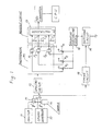
- Fig. 1 schematically shows one embodiment of the invention, which comprises a spark generator 10, an ignitor 11, a spectrometer 12, a photosensor PS and a readout circuit 13.
- a sample 14 to be analyzed and an electrode 15 are juxtaposed across an analytical gap g , with the ignitor 11 being connected thereto through a trigger spark gap g ′.
- the photosensor PS comprises a plurality of photomultiplier tubes P1, P2, ⁇ P n arranged at predetermined wavelength positions on the spectral plane of the spectrometer 12.
- a negative high-voltage source 16 is connected to the dynodes of the photomultiplier tubes P1 , P2, ⁇ P n through sensitivity attenuators R1, R2, ⁇ R n , respectively.
- the readout circuit 13 comprises a plurality of capacitors C1, C2, ⁇ C n and a multiplexer 20.
- the outputs of the photomultiplier tubes P1, P2, ⁇ P n are stored in the capacitors C1, C2, ⁇ C n , respectively, the outputs of which are applied to a computer CPU through the multiplexer 20 and an analog/digital converter A/D.
- a photodetector 17 is provided adjacent the trigger spark gap g ′ to detect the light caused by a trigger discharge and produce a detection pulse, which is applied to a timing circuit 18 which comprises a series combination of two one-shot circuits.
- the timing circuit 18 produces one output pulse having a certain width a certain period of time after the detection pulse from the photodetector 17 is applied thereto.
- the output pulse from the timing circuit 18 renders conducting a switching circuit 19 connected between the negative high-voltage source 16 and the ground.
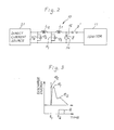
- Fig. 2 schematically shows an example of the spark generator 10, which comprises capacitors K1 and K2 for storing energy to be discharged, inductors L1 and L2 with a protective diode D1, D2 connected across each of the capacitors, and a direct current source 21 which charges the capacitors.
- the capacitor K1 is connected to the analytical gap g through the inductor L1
- the capacitor K2 is connected to the analytical gap g through the series combination of inductors L1 and L2.
- the ignitor 11 is connected across the analytical gap g through the trigger spark gap g ′.
- the discharge current breaks the insulation of the analytical gap g and passes therethrough, whereupon the electric charge stored in the capacitors K1 and K2 is discharged through the analytical gap g . Since the electric charge of the capacitor K2 is discharged through the inductors L1 and L2 connected in series, the discharge is conducted slowly. On the other hand, since the electric charge of the capacitor K1 is discharged through the inductor L1 only, the discharge is conducted quickly. In other words, the charge of the capacitor K1 is discharged first and then the charge of the capacitor K2 is discharged. With the capacitor K1 of a larger capacity than that of the capacitor K2, it is possible to supply a larger amount of energy from the first capacitor K1 and a smaller amount of energy from the second capacitor K2.
- Fig. 3 shows a waveform of a spark discharge generated in the analytical gap g .
- each of the spark discharges generated in the analytical gap for one operation of analysis of a sample comprises a high-energy portion e1 and a low-energy portion e2 continuing from the high-energy portion.
- the timing circuit 18 receives the detection pulse when the photodetector 17 detects a trigger spark discharge e t at t1 and after a period of time corresponding to the high-energy portion e1 of the spark discharge in the analytical gap, the timing circuit 18 produces an output pulse a at t2 to close the switching circuit 19 thereby to cause the negative high-voltage source 16 to activate the photomultiplier tubes P1 ⁇ P n , which detect the corresponding emission lines in the spectrum of the sample caused by the low-energy portion e2 of the spark discharge and produce corresponding electrical signals.
- a negative high voltage is impressed on the dynodes of the photomultiplier tubes only during the low-energy excitation of the sample. It is also possible to prevent impression of a negative high voltage on the dynodes only during the high-energy excitation of the sample.
- Fig. 4 shows another embodiment of the invention, wherein a laser is used for vaporization of the sample.
- the apparatus comprises a laser source 30, a circuit 31 for driving the source 30 to produce pulses of high-energy laser beam at a predetermined cycle, and a lense 32 for focusing the laser beam onto a point on the surface of a sample 14 thereby to cause the material of the sample at the point to vaporize.
- a beam detector 17 At one side of the laser beam there is provided a beam detector 17 which detects each pulse of the laser beam to produce a detection signal, which triggers the timing circuit 18.
- the circuit Upon passage of a time preset in the timing circuit, the circuit produces an output signal to cause the spark generator 10 to produce a low-energy spark discharge in the analytical gap g between the sample 14 and the electrode 15.
- the output from the timing circuit 18 is also applied to the switching circuit 19 to close the circuit thereby to cause the negative high-voltage source 16 to activate the photomultiplier tubes P1 ⁇ P n to operate in the same manner as described with reference to Fig. 1.
- Fig. 5 shows a third embodiment of the invention wherein a laser is used for both high-energy and low-energy excitation of the sample.
- the driving circuit 31 in Fig. 5 is so designed as to cause the laser source 30 to produce laser pulses each having a high-energy protion and a low-energy portion such as shown in Fig. 3.
- the timing circuit 18 Upon passage of a period of time corresponding to the high-energy excitation after the photodetector 17 detects the high-energy portion of each laser pulse, the timing circuit 18 produces an output pulse to close the switching circuit 19, whereupon the negative high-voltage source impresses a negative high voltage on the dynodes of the photomultiplier tubes P1 ⁇ P n for activation thereof.
- the same reference numerals as in Fig. 1 or 4 designate corresponding elements in Fig. 1 or 4, and the readout circuit 13 operates in substantially the same manner as in the previous embodiments.
- each of a number of emissions of light from the sample for one operation of analysis is caused by both high-energy and low-energy excitation of the sample, and no preparatory discharge need be conducted on the sample. Since high-energy excitation is immediately followed by low-energy excitation, it is possible with a smaller amount of energy than otherwise to cause the sample vapor to emit light, with resulting reduction of the background noise, improvement of the sensitivity and precision of analysis, and reduction of the manufacturing cost of the apparatus.
- Apparatus for emission spectrochemical analysis of a sample containing elements to be analyzed wherein the sample is cyclically excited with relatively high energy to vaporize the sample elements and successively with relatively low energy to cause the vapori zed elements to emit light containing spectral lines characteristic of the elements, which spectral lines are detected by a plurality of photomultiplier tubes corresponding to the spectral lines, with a common negative high-voltage source connected to the dynodes of the photomultiplier tubes.
- the negative high-voltage source is controlled in such a manner that it supplies a negative high voltage to the dynodes of the photomultiplier tubes to activate the tubes only during the low-energy excitation of the sample.
Abstract
Description
- This invention relates generally to emission spectroscopy and more particularly to an apparatus for emission spectrochemical analysis which utilizes spark discharges or pulses of a laser beam.
- There is known a method of emission spectrochemical analysis in which spark discharges or pulses of a laser beam are applied to a sample to be analyzed to cause the sample to emit light, which is analyzed spectroscopically. The method has the following problem: In emission spectrochemical analysis using spark discharge, it is customary to pretreat the surface of a sample to be analyzed by applying spark discharges to the sample surface before analysis is conducted so as to reduce the adverse influence of small scars and/or pinpholes on or in the sample surface and/or foreign matters, thereby improving the precision of analysis. For example, for analysis of a sample for 5 seconds the sample must be pretreated with high-energy spark discharges for more than 10 seconds.
- The spark discharges for pretreatment of a sample may be referred to as the "preparatory discharges", while the spark discharges for analysis may be referred to as the "analytic discharges".
- The reason why the preparatory discharge and the analytic discharge are conducted separately is as follows: Although high-energy discharge has a great capacity for vaporizing a sample, the resulting background light is strong as compared with the spectral line intensity of the component elements of the sample, with resulting decrease in the sensitivity of analysis. Therefore, low-energy discharge is suitable for analysis itself. Thus, after high-energy preparatory discharges have been conducted on a sample for 5 to 10 seconds, several thousand low-energy analytic discharges are conducted to analyze the light from the sample.
- If the energy for analytic discharge is too low, however, the amount of the sample components vaporized decreases and the intensity of the light of the spectral emission lines produced becomes weak, with resulting reduction of the sensitivity and precision of analysis. Therefore, a sufficient amount of the sample must be vaporized by analytic discharges, so that there is a limit to which the energy level of the analytic discharges can be lowered, with resulting difficulty in reducing the background light.
- As mentioned above, the time required for preparatory discharges is longer than the time required for analytic discharges. The reason why this is so is that the position in the surface of a sample which is struck by each of the spark discharges produced in one operation of analysis is uncertain, so that the whole area of the sample surface must be treated beforehand by preparatory discharges. To improve the precision of analysis a longer period of time is required for preparatory discharge.
- Since a sufficient amount of the sample must be vaporized in analytic discharge, the energy for analytic discharge cannot be reduced to a very low level, with resulting difficulty in reducing the background light and obtaining a high sensitivity.
- The present inventors have once proposed a method of spectrochemical analysis of a sample containing elements to be analyzed, in which high-energy pulses are cyclically applied onto a small area of a sample to vaporize the components of the sample from the small area thereof, and low-energy spark discharges are generated by a spark generator including an electrode facing the sample so as to be applied to the small area of the sample a predetermined period of time after the application of each high-energy pulse and during the time in which the vaporized components of the sample caused by the application of high energy remains between the sample and the electrode, and the light emitted by the sample vapor while the low-energy spark discharges are being conducted is spectroscopically measured.
- The characteristic of the above-mentioned prior invention is that each and every one of the emissions of light from the sample being analyzed comprises a step of vaporizing the sample and that of analyzing the vaporized elements of the sample. With the method of the prior invention, it is possible to analyze a sample at a cleaned spot on the surface thereof by low-energy spark discharge without pretreatment by conventional preparatory discharge, and to obtain a high sensitivity due to the lowered background level. The circuit arrangement, however, is complicated. In the prior art arrangement the output from the measuring circuit is amplified and sampled by a switching circuit operated synchronously with each emission of light from the sample, and one measuring channel must be provided for each one of the spectral lines of the elements in the sample, and one switching circuit is required for each measuring channel, with resulting complication of the whole circuit arrangement.
- Accordingly, the primary object of the invention is to simplify the circuit arrangement used in an apparatus for emission spectrochemical analysis which uses a time resolution method of measuring the spectral intensity of light emissions from a sample caused by spark discharge pulses each comprising a high-energy and a low-energy portion.
- Briefly stated, the apparatus of the invention comprises: means for cyclically exciting a sample with relatively high energy to vaporize the elements contained in the sample to be analyzed and successively with relatively low energy to cause the vaporized elements to emit light; means for dispersing the light emitted by the vaporized elements to produce a spectrum containing spectral lines characteristic of the elements; a plurality of photomultiplier tubes each so arranged as to receive the light of one of the spectral lines to produce a corresponding electrical signal; a negative high-voltage source; and means for controlling the negative high voltage source to impress a negative high voltage upon the dynodes of the photomultiplier tubes during the low-energy excitation of the sample, so that the photomultiplier tubes receive the light of the spectral lines to produce a corresponding electrical signal, while preventing the negative high voltage from being impressed' upon the dynodes during the highenergy excitation of the sample.
- The photomultiplier tubes are rendered inoperative by cutting off the negative high voltage impressed on the dynodes of the photomultiplier tubes. Since the common negative high-voltage source supplies a voltage to the dynodes of the photomultiplier tubes in the measuring channels, by switching on or off the negative high-voltage source it is possible to control the operation of the photomultiplier tubes in all the measuring channels simultaneously, so that a single switching circuit suffices. with resulting simplification of the circuit arrangement of the apparatus.
-
- Fig. 1 is a block diagram schematically showing one embodiment of the invention;
- Fig. 2 is an electrical circuit diagram of a portion of Fig. 1;
- Fig. 3 is a waveform diagram for explanation of the operation of the apparatus of the invention;
- Fig. 4 is a block diagram schematically showing another embodiment of the invention; and
- Fig. 5 is a block diagram schematically showing a third embodiment of the invention.
- Fig. 1 schematically shows one embodiment of the invention, which comprises a
spark generator 10, anignitor 11, aspectrometer 12, a photosensor PS and areadout circuit 13. Asample 14 to be analyzed and anelectrode 15 are juxtaposed across an analytical gap g, with theignitor 11 being connected thereto through a trigger spark gap g′. - The photosensor PS comprises a plurality of photomultiplier tubes P₁, P₂, ··· Pn arranged at predetermined wavelength positions on the spectral plane of the
spectrometer 12. A negative high-voltage source 16 is connected to the dynodes of the photomultiplier tubes P₁ , P₂, ··· Pn through sensitivity attenuators R₁, R₂, ··· Rn, respectively. Thereadout circuit 13 comprises a plurality of capacitors C₁, C₂, ··· Cn and amultiplexer 20. The outputs of the photomultiplier tubes P₁, P₂, ··· Pn are stored in the capacitors C₁, C₂, ··· Cn, respectively, the outputs of which are applied to a computer CPU through themultiplexer 20 and an analog/digital converter A/D. - A
photodetector 17 is provided adjacent the trigger spark gap g′ to detect the light caused by a trigger discharge and produce a detection pulse, which is applied to atiming circuit 18 which comprises a series combination of two one-shot circuits. Thetiming circuit 18 produces one output pulse having a certain width a certain period of time after the detection pulse from thephotodetector 17 is applied thereto. The output pulse from thetiming circuit 18 renders conducting aswitching circuit 19 connected between the negative high-voltage source 16 and the ground. - The instant a spark is generated in the trigger spark gap g′ , a spark discharge is triggered in the analytical gap g of the
spark generator 10. Therefore, by detecting the light caused to emit by a spark in the trigger spark gap g′ and rendering theswitching circuit 19 conducting for a predetermined period of time after a certain period of time, it is possible to sample the output from the photomultiplier tubes P₁, P₂ . . . Pn for a predetermined period of time during the discharge in the analytical gap. - Fig. 2 schematically shows an example of the
spark generator 10, which comprises capacitors K₁ and K₂ for storing energy to be discharged, inductors L₁ and L₂ with a protective diode D₁, D₂ connected across each of the capacitors, and a directcurrent source 21 which charges the capacitors. The capacitor K₁ is connected to the analytical gap g through the inductor L₁ , and the capacitor K₂ is connected to the analytical gap g through the series combination of inductors L1 and L2. Theignitor 11 is connected across the analytical gap g through the trigger spark gap g′. - When a discharge is generated in the trigger spark gap g′ by a trigger pulse produced by the
ignitor 11, the discharge current breaks the insulation of the analytical gap g and passes therethrough, whereupon the electric charge stored in the capacitors K₁ and K₂ is discharged through the analytical gap g. Since the electric charge of the capacitor K₂ is discharged through the inductors L₁ and L₂ connected in series, the discharge is conducted slowly. On the other hand, since the electric charge of the capacitor K₁ is discharged through the inductor L₁ only, the discharge is conducted quickly. In other words, the charge of the capacitor K₁ is discharged first and then the charge of the capacitor K₂ is discharged. With the capacitor K₁ of a larger capacity than that of the capacitor K₂, it is possible to supply a larger amount of energy from the first capacitor K₁ and a smaller amount of energy from the second capacitor K₂. - Fig. 3 shows a waveform of a spark discharge generated in the analytical gap g. As shown in the figure each of the spark discharges generated in the analytical gap for one operation of analysis of a sample comprises a high-energy portion e₁ and a low-energy portion e₂ continuing from the high-energy portion. The
timing circuit 18 receives the detection pulse when thephotodetector 17 detects a trigger spark discharge et at t₁ and after a period of time corresponding to the high-energy portion e₁ of the spark discharge in the analytical gap, thetiming circuit 18 produces an output pulse a at t₂ to close theswitching circuit 19 thereby to cause the negative high-voltage source 16 to activate the photomultiplier tubes P₁∼Pn, which detect the corresponding emission lines in the spectrum of the sample caused by the low-energy portion e₂ of the spark discharge and produce corresponding electrical signals. - In the above embodiment a negative high voltage is impressed on the dynodes of the photomultiplier tubes only during the low-energy excitation of the sample. It is also possible to prevent impression of a negative high voltage on the dynodes only during the high-energy excitation of the sample.
- Fig. 4 shows another embodiment of the invention, wherein a laser is used for vaporization of the sample. In Fig. 4 the same reference numerals as in Fig. 1 designate corresponding elements in Fig. 1, so that no explanation will be given to them except when necessary. The apparatus comprises a
laser source 30, acircuit 31 for driving thesource 30 to produce pulses of high-energy laser beam at a predetermined cycle, and alense 32 for focusing the laser beam onto a point on the surface of asample 14 thereby to cause the material of the sample at the point to vaporize. At one side of the laser beam there is provided abeam detector 17 which detects each pulse of the laser beam to produce a detection signal, which triggers thetiming circuit 18. Upon passage of a time preset in the timing circuit, the circuit produces an output signal to cause thespark generator 10 to produce a low-energy spark discharge in the analytical gap g between thesample 14 and theelectrode 15. The output from thetiming circuit 18 is also applied to the switchingcircuit 19 to close the circuit thereby to cause the negative high-voltage source 16 to activate the photomultiplier tubes P₁∼Pn to operate in the same manner as described with reference to Fig. 1. - Fig. 5 shows a third embodiment of the invention wherein a laser is used for both high-energy and low-energy excitation of the sample. To this end, the driving
circuit 31 in Fig. 5 is so designed as to cause thelaser source 30 to produce laser pulses each having a high-energy protion and a low-energy portion such as shown in Fig. 3. Upon passage of a period of time corresponding to the high-energy excitation after thephotodetector 17 detects the high-energy portion of each laser pulse, thetiming circuit 18 produces an output pulse to close the switchingcircuit 19, whereupon the negative high-voltage source impresses a negative high voltage on the dynodes of the photomultiplier tubes P₁∼Pn for activation thereof. In Fig. 5 the same reference numerals as in Fig. 1 or 4 designate corresponding elements in Fig. 1 or 4, and thereadout circuit 13 operates in substantially the same manner as in the previous embodiments. - In accordance with the invention, it is possible to simplify the circuit arrangement for emission spectrochemical analysis of a sample wherein each of a number of emissions of light from the sample for one operation of analysis is caused by both high-energy and low-energy excitation of the sample, and no preparatory discharge need be conducted on the sample. Since high-energy excitation is immediately followed by low-energy excitation, it is possible with a smaller amount of energy than otherwise to cause the sample vapor to emit light, with resulting reduction of the background noise, improvement of the sensitivity and precision of analysis, and reduction of the manufacturing cost of the apparatus.
- Apparatus for emission spectrochemical analysis of a sample containing elements to be analyzed, wherein the sample is cyclically excited with relatively high energy to vaporize the sample elements and successively with relatively low energy to cause the vapori zed elements to emit light containing spectral lines characteristic of the elements, which spectral lines are detected by a plurality of photomultiplier tubes corresponding to the spectral lines, with a common negative high-voltage source connected to the dynodes of the photomultiplier tubes. The negative high-voltage source is controlled in such a manner that it supplies a negative high voltage to the dynodes of the photomultiplier tubes to activate the tubes only during the low-energy excitation of the sample.
Claims (6)
- (1) Apparatus for emission spectrochemical analysis of a sample containing elements to be analyzed, comprising:
means for cyclically exciting said sample with relatively high energy to vaporize said elements contained in said sample and successively with relatively low energy to cause said vaporized elements to emit light;
means for dispersing the light emitted by said vaporized elements to produce a spectrum containing spectral lines characteristic of said elements;
a plurality of photomultiplier tubes each so arranged as to receive the light of one of said spectral lines to produce a corresponding electrical signal;
a negative high-voltage source; and
means for controlling said, negative high-voltage source to impress a negative high voltage upon the dynodes of said photomultiplier tubes during said low-energy excitation of said sample, so that said photomultiplier tubes receive said light of said spectral lines to produce a corresponding electrical signal, while preventing said negative high voltage from being impressed upon said dynodes during said high-energy excitation of said sample. - (2) The apparatus of claim 1, wherein said exciting means comprises means for producing spark discharges each having a waveform which comprises a relatively high-energy portion and a relatively low-energy portion continuing from said high-energy portion.
- (3) The apparatus of claim 1, wherein said exciting means comprises a laser for producing a laser beam to be applied to said sample to vaporize said elements contained therein and a spark generator to generate a spark to cause said vaporized elements to emit light.
- (4) The apparatus of claim 1, wherein said exciting means comprises a laser for producing a laser beam of high energy to be applied to said sample to vaporize said elements contained therein and a laser beam of low energy to be applied to said vaporized elements to cause emission of light therefrom.
- (5) The apparatus of claim 1, wherein said controlling means comprises a single normally open switching circuit connected between said negative high-voltage source and the ground, and means for causing said switching circuit to be closed during said low-energy excitation of said sample thereby to cause said negative high-voltage source to activate said photomultiplier tubes.
- (6) The apparatus of claim 1, wherein said controlling means comprises a single normally closed switching circuit connected between said negative high-voltage source and the ground, and means for causing said switching circuit to be opened during said high-energy excitation of said sample thereby to prevent said negative high-voltage source to activate said photomultiplier tubes.
Applications Claiming Priority (2)
| Application Number | Priority Date | Filing Date | Title |
|---|---|---|---|
| JP145712/89 | 1989-06-08 | ||
| JP1145712A JPH0676967B2 (en) | 1989-06-08 | 1989-06-08 | Luminescence analyzer |
Publications (3)
| Publication Number | Publication Date |
|---|---|
| EP0401470A2 true EP0401470A2 (en) | 1990-12-12 |
| EP0401470A3 EP0401470A3 (en) | 1991-03-20 |
| EP0401470B1 EP0401470B1 (en) | 1997-05-28 |
Family
ID=15391381
Family Applications (1)
| Application Number | Title | Priority Date | Filing Date |
|---|---|---|---|
| EP90103719A Expired - Lifetime EP0401470B1 (en) | 1989-06-08 | 1990-02-26 | Apparatus for emission spectrochemical analysis |
Country Status (5)
| Country | Link |
|---|---|
| US (1) | US5216482A (en) |
| EP (1) | EP0401470B1 (en) |
| JP (1) | JPH0676967B2 (en) |
| CN (1) | CN1027520C (en) |
| DE (1) | DE69030785T2 (en) |
Cited By (3)
| Publication number | Priority date | Publication date | Assignee | Title |
|---|---|---|---|---|
| EP0501476A2 (en) * | 1991-02-28 | 1992-09-02 | Shimadzu Corporation | Spectroscopic analysis method and analyzing system |
| EP1110076A1 (en) * | 1998-09-04 | 2001-06-27 | Generation Technology Research Pty Ltd | Laser-induced ionisation spectroscopy, particularly for coal |
| EP1351049A3 (en) * | 2002-04-01 | 2004-02-25 | Central Iron & Steel Research Institute | Analyzer for metal |
Families Citing this family (14)
| Publication number | Priority date | Publication date | Assignee | Title |
|---|---|---|---|---|
| JPH04326043A (en) * | 1991-04-25 | 1992-11-16 | Shimadzu Corp | Emission light spectrum analizer |
| DE19651677A1 (en) * | 1996-12-12 | 1998-06-18 | Spectro Analytical Instr | Optical emission spectrometer |
| DE19753348A1 (en) * | 1997-12-03 | 1999-06-10 | Spectro Analytical Instr Gmbh | Analysis apparatus for high-temperature plasma pulse |
| US20030189456A1 (en) * | 2002-01-08 | 2003-10-09 | Foster Thomas H. | TTl controller system for one or more devices and a method thereof |
| US7391508B2 (en) * | 2005-07-20 | 2008-06-24 | Thermo Niton Analyzers Llc | Arc/spark optical emission spectroscopy correlated with spark location |
| US9072169B1 (en) | 2010-07-13 | 2015-06-30 | Cascodium Inc. | Pulse generator and systems and methods for using same |
| CN102384784B (en) * | 2010-09-01 | 2015-05-20 | 北京普源精电科技有限公司 | Spectrophotometer capable of dynamically adjusting system energy and dynamic adjusting method thereof |
| DE102011114874A1 (en) * | 2011-09-30 | 2013-04-04 | Carl Zeiss Microscopy Gmbh | Evaluation circuit for an optoelectronic detector and method for recording fluorescence events |
| JP5974696B2 (en) * | 2012-07-13 | 2016-08-23 | Jfeスチール株式会社 | Segregation evaluation method and segregation evaluation apparatus by emission spectroscopic analysis |
| CN103969245B (en) * | 2014-05-20 | 2016-03-23 | 江苏鑫知源仪器有限公司 | A kind of vacuum photo-electric direct reading spectrometer |
| DE102014010185A1 (en) * | 2014-07-09 | 2016-01-14 | Carl Zeiss Microscopy Gmbh | Method for operating a laser scanning microscope |
| CN104267004B (en) * | 2014-10-24 | 2018-04-24 | 合肥市再德高分子材料有限公司 | A kind of sample stimulation system of photoelectric direct-reading spectrograph |
| CN106442433A (en) * | 2016-09-29 | 2017-02-22 | 哈尔滨理工大学 | Polymer breakdown luminescent spectrum measurement system based on ICCD imaging |
| DE102019100290B4 (en) * | 2019-01-08 | 2020-12-03 | Spectro Analytical Instruments Gmbh | Spectrometer with mechanical shutter |
Citations (3)
| Publication number | Priority date | Publication date | Assignee | Title |
|---|---|---|---|---|
| GB1066431A (en) * | 1962-09-27 | 1967-04-26 | Hilger & Watts Ltd | Improvements in or relating to methods of and means for spectrochemical analysis |
| EP0038549A1 (en) * | 1980-04-22 | 1981-10-28 | Forschungszentrum Jülich Gmbh | Method and device for spectrometric detection of elements on the surface of a solid body |
| EP0318900A2 (en) * | 1987-11-30 | 1989-06-07 | Shimadzu Corporation | Method and apparatus for emission spectroscopis analysis |
Family Cites Families (3)
| Publication number | Priority date | Publication date | Assignee | Title |
|---|---|---|---|---|
| US3531202A (en) * | 1966-11-14 | 1970-09-29 | Baird Atomic Inc | Spectrometer readout system |
| US4393327A (en) * | 1981-07-29 | 1983-07-12 | Wisconsin Alumni Research Foundation | Electric spark type light source for producing light for spectroscopic analysis |
| JPS59182344A (en) * | 1983-03-31 | 1984-10-17 | Shimadzu Corp | Emission spectrochemical analysis device |
-
1989
- 1989-06-08 JP JP1145712A patent/JPH0676967B2/en not_active Expired - Fee Related
- 1989-11-29 CN CN89108991A patent/CN1027520C/en not_active Expired - Fee Related
-
1990
- 1990-02-23 US US07/483,628 patent/US5216482A/en not_active Expired - Fee Related
- 1990-02-26 DE DE69030785T patent/DE69030785T2/en not_active Expired - Fee Related
- 1990-02-26 EP EP90103719A patent/EP0401470B1/en not_active Expired - Lifetime
Patent Citations (3)
| Publication number | Priority date | Publication date | Assignee | Title |
|---|---|---|---|---|
| GB1066431A (en) * | 1962-09-27 | 1967-04-26 | Hilger & Watts Ltd | Improvements in or relating to methods of and means for spectrochemical analysis |
| EP0038549A1 (en) * | 1980-04-22 | 1981-10-28 | Forschungszentrum Jülich Gmbh | Method and device for spectrometric detection of elements on the surface of a solid body |
| EP0318900A2 (en) * | 1987-11-30 | 1989-06-07 | Shimadzu Corporation | Method and apparatus for emission spectroscopis analysis |
Non-Patent Citations (2)
| Title |
|---|
| ANALYTICAL CHEMISTRY, vol. 52, no. 4, Apil 1980, pages 746-753, Ohio, US; D.M. COLEMAN et al.: "High frequency excitation of spark-sampled metal vapor" * |
| TECHNICAL DIGEST, no. 35, July 1974, Western Electric; T.H. BRIGGS et al.: "Direct reading laser spectrometer" * |
Cited By (7)
| Publication number | Priority date | Publication date | Assignee | Title |
|---|---|---|---|---|
| EP0501476A2 (en) * | 1991-02-28 | 1992-09-02 | Shimadzu Corporation | Spectroscopic analysis method and analyzing system |
| EP0501476A3 (en) * | 1991-02-28 | 1993-02-17 | Shimadzu Corporation | Spectroscopic analysis method and analyzing system |
| US5363189A (en) * | 1991-02-28 | 1994-11-08 | Shimadzu Corporation | Spectroscopic analysis method and analyzing system |
| EP1110076A1 (en) * | 1998-09-04 | 2001-06-27 | Generation Technology Research Pty Ltd | Laser-induced ionisation spectroscopy, particularly for coal |
| EP1110076A4 (en) * | 1998-09-04 | 2003-09-17 | Generation Technology Res Pty | Laser-induced ionisation spectroscopy, particularly for coal |
| US6771368B1 (en) | 1998-09-04 | 2004-08-03 | Generation Technology Research Pty Ltd. | Laser-induced ionisation spectroscopy, particularly for coal |
| EP1351049A3 (en) * | 2002-04-01 | 2004-02-25 | Central Iron & Steel Research Institute | Analyzer for metal |
Also Published As
| Publication number | Publication date |
|---|---|
| JPH0676967B2 (en) | 1994-09-28 |
| CN1047923A (en) | 1990-12-19 |
| DE69030785T2 (en) | 1997-12-04 |
| US5216482A (en) | 1993-06-01 |
| CN1027520C (en) | 1995-01-25 |
| JPH0310148A (en) | 1991-01-17 |
| EP0401470A3 (en) | 1991-03-20 |
| EP0401470B1 (en) | 1997-05-28 |
| DE69030785D1 (en) | 1997-07-03 |
Similar Documents
| Publication | Publication Date | Title |
|---|---|---|
| US5216482A (en) | Apparatus for emission spectrochemical analysis | |
| US7821634B2 (en) | Laser-triggered plasma apparatus for atomic emission spectroscopy | |
| US4898466A (en) | Method and apparatus for emission spectroscopic analysis | |
| EP0396291B1 (en) | Apparatus and methods for optical emission spectroscopy | |
| Casini et al. | Time-resolved LIBS experiment for quantitative determination of pollutant concentrations in air | |
| US4461572A (en) | Instrument for measuring light emission induced by repetitive stimulation of the same type | |
| CN107064111B (en) | High-repetition-frequency laser stripping-spark induced breakdown spectroscopy element analysis system and method | |
| US6034768A (en) | Induced breakdown spectroscopy detector system with controllable delay time | |
| US5088820A (en) | Laser enhanced ionization detector for Raman spectroscopy | |
| DE4341462A1 (en) | Measuring the material composition of substances | |
| JP5150824B2 (en) | Fuel concentration measuring device, fuel concentration measuring method, and calibration curve preparing method therefor | |
| US5141314A (en) | Spectroanalytical system | |
| EP2377246B1 (en) | Apparatus and methods for optical emission spectroscopy | |
| US4438329A (en) | Minimizing the effect of spurious photodetector currents in flash spectrofluorimetry | |
| Chen et al. | Excitation of the B Π g 3 states of N 2 by electron impact | |
| JP2713272B2 (en) | Emission spectrometer | |
| CN109870235B (en) | Optical emission spectrometer, method for operating the same and use thereof | |
| KR20030054084A (en) | Method of laser-induced plasma atomic emission spectroscopy and apparatus thereof | |
| KR900005330B1 (en) | Measuring method for inoragnic element | |
| Klein et al. | Luminescence of high pressure argon excited by pulsed electric discharges | |
| Chan et al. | Characterization of a Low-Temperature Plasma (LTP) Ambient Ionization Source Using Temporally Resolved Monochromatic Imaging Spectrometry | |
| JPH039259A (en) | Mass spectrometer by high-repetition laser stimulation | |
| Gorbatenko et al. | Signal formation in laser-enhanced atomic ionization spectrometry with laser sampling into the flame | |
| JPS58211632A (en) | Method and device for measuring laser excited fluorescence | |
| Kalev et al. | Statistical model for assessing the optical density of laser-produced microplasma |
Legal Events
| Date | Code | Title | Description |
|---|---|---|---|
| PUAI | Public reference made under article 153(3) epc to a published international application that has entered the european phase |
Free format text: ORIGINAL CODE: 0009012 |
|
| AK | Designated contracting states |
Kind code of ref document: A2 Designated state(s): DE FR GB |
|
| PUAL | Search report despatched |
Free format text: ORIGINAL CODE: 0009013 |
|
| 17P | Request for examination filed |
Effective date: 19901231 |
|
| AK | Designated contracting states |
Kind code of ref document: A3 Designated state(s): DE FR GB |
|
| 17Q | First examination report despatched |
Effective date: 19941025 |
|
| GRAG | Despatch of communication of intention to grant |
Free format text: ORIGINAL CODE: EPIDOS AGRA |
|
| GRAH | Despatch of communication of intention to grant a patent |
Free format text: ORIGINAL CODE: EPIDOS IGRA |
|
| GRAH | Despatch of communication of intention to grant a patent |
Free format text: ORIGINAL CODE: EPIDOS IGRA |
|
| GRAA | (expected) grant |
Free format text: ORIGINAL CODE: 0009210 |
|
| AK | Designated contracting states |
Kind code of ref document: B1 Designated state(s): DE FR GB |
|
| REF | Corresponds to: |
Ref document number: 69030785 Country of ref document: DE Date of ref document: 19970703 |
|
| ET | Fr: translation filed | ||
| PGFP | Annual fee paid to national office [announced via postgrant information from national office to epo] |
Ref country code: GB Payment date: 19980202 Year of fee payment: 9 |
|
| PGFP | Annual fee paid to national office [announced via postgrant information from national office to epo] |
Ref country code: FR Payment date: 19980216 Year of fee payment: 9 |
|
| PGFP | Annual fee paid to national office [announced via postgrant information from national office to epo] |
Ref country code: DE Payment date: 19980331 Year of fee payment: 9 |
|
| PLBE | No opposition filed within time limit |
Free format text: ORIGINAL CODE: 0009261 |
|
| STAA | Information on the status of an ep patent application or granted ep patent |
Free format text: STATUS: NO OPPOSITION FILED WITHIN TIME LIMIT |
|
| 26N | No opposition filed | ||
| PG25 | Lapsed in a contracting state [announced via postgrant information from national office to epo] |
Ref country code: GB Free format text: LAPSE BECAUSE OF NON-PAYMENT OF DUE FEES Effective date: 19990226 |
|
| GBPC | Gb: european patent ceased through non-payment of renewal fee |
Effective date: 19990226 |
|
| PG25 | Lapsed in a contracting state [announced via postgrant information from national office to epo] |
Ref country code: FR Free format text: LAPSE BECAUSE OF NON-PAYMENT OF DUE FEES Effective date: 19991029 |
|
| PG25 | Lapsed in a contracting state [announced via postgrant information from national office to epo] |
Ref country code: DE Free format text: LAPSE BECAUSE OF NON-PAYMENT OF DUE FEES Effective date: 19991201 |
|
| REG | Reference to a national code |
Ref country code: FR Ref legal event code: ST |