EP0400378A2 - Leiterplattensockel mit Kleeblattkontakt - Google Patents
Leiterplattensockel mit Kleeblattkontakt Download PDFInfo
- Publication number
- EP0400378A2 EP0400378A2 EP90108923A EP90108923A EP0400378A2 EP 0400378 A2 EP0400378 A2 EP 0400378A2 EP 90108923 A EP90108923 A EP 90108923A EP 90108923 A EP90108923 A EP 90108923A EP 0400378 A2 EP0400378 A2 EP 0400378A2
- Authority
- EP
- European Patent Office
- Prior art keywords
- terminal
- upwardly
- panel
- beams
- base
- Prior art date
- Legal status (The legal status is an assumption and is not a legal conclusion. Google has not performed a legal analysis and makes no representation as to the accuracy of the status listed.)
- Granted
Links
- 238000003780 insertion Methods 0.000 claims description 6
- 230000037431 insertion Effects 0.000 claims description 6
- 229910052751 metal Inorganic materials 0.000 claims description 3
- 239000002184 metal Substances 0.000 claims description 3
- 239000000463 material Substances 0.000 description 2
- 230000000087 stabilizing effect Effects 0.000 description 2
- 229910000906 Bronze Inorganic materials 0.000 description 1
- OAICVXFJPJFONN-UHFFFAOYSA-N Phosphorus Chemical compound [P] OAICVXFJPJFONN-UHFFFAOYSA-N 0.000 description 1
- 108010038083 amyloid fibril protein AS-SAM Proteins 0.000 description 1
- DMFGNRRURHSENX-UHFFFAOYSA-N beryllium copper Chemical compound [Be].[Cu] DMFGNRRURHSENX-UHFFFAOYSA-N 0.000 description 1
- 239000010974 bronze Substances 0.000 description 1
- 230000001010 compromised effect Effects 0.000 description 1
- KUNSUQLRTQLHQQ-UHFFFAOYSA-N copper tin Chemical compound [Cu].[Sn] KUNSUQLRTQLHQQ-UHFFFAOYSA-N 0.000 description 1
- 230000009977 dual effect Effects 0.000 description 1
- 229920006351 engineering plastic Polymers 0.000 description 1
- 239000007787 solid Substances 0.000 description 1
Images


Classifications
-
- H—ELECTRICITY
- H01—ELECTRIC ELEMENTS
- H01R—ELECTRICALLY-CONDUCTIVE CONNECTIONS; STRUCTURAL ASSOCIATIONS OF A PLURALITY OF MUTUALLY-INSULATED ELECTRICAL CONNECTING ELEMENTS; COUPLING DEVICES; CURRENT COLLECTORS
- H01R12/00—Structural associations of a plurality of mutually-insulated electrical connecting elements, specially adapted for printed circuits, e.g. printed circuit boards [PCB], flat or ribbon cables, or like generally planar structures, e.g. terminal strips, terminal blocks; Coupling devices specially adapted for printed circuits, flat or ribbon cables, or like generally planar structures; Terminals specially adapted for contact with, or insertion into, printed circuits, flat or ribbon cables, or like generally planar structures
- H01R12/70—Coupling devices
- H01R12/71—Coupling devices for rigid printing circuits or like structures
- H01R12/72—Coupling devices for rigid printing circuits or like structures coupling with the edge of the rigid printed circuits or like structures
- H01R12/721—Coupling devices for rigid printing circuits or like structures coupling with the edge of the rigid printed circuits or like structures cooperating directly with the edge of the rigid printed circuits
-
- H—ELECTRICITY
- H01—ELECTRIC ELEMENTS
- H01R—ELECTRICALLY-CONDUCTIVE CONNECTIONS; STRUCTURAL ASSOCIATIONS OF A PLURALITY OF MUTUALLY-INSULATED ELECTRICAL CONNECTING ELEMENTS; COUPLING DEVICES; CURRENT COLLECTORS
- H01R13/00—Details of coupling devices of the kinds covered by groups H01R12/70 or H01R24/00 - H01R33/00
- H01R13/02—Contact members
- H01R13/10—Sockets for co-operation with pins or blades
- H01R13/11—Resilient sockets
Definitions
- This application relates to an electrical connector and a terminal for use in the electrical connector of the type suitable for use in establishing an interconnector to traces on a circuit panel, especially to an electrical connector socket for use in establishing electrical interconnections to a single in-line memory module.
- Single in-line memory modules represent a high density, low profile single in-line package for electronic components such as dynamic random access memory integrated circuit components.
- a plurality of these components can be mounted in line on a circuit panel whose height is little more than the length of the components themselves.
- the circuit panels can in turn be mounted on a printed circuit board daughtercard which can then be mounted on a printed circuit board mothercard. The spacing between adjacent daughtercards would then need to be only slightly greater than the height of the individual circuit panels or single in-line memory modules.
- One approach for mounting single in-line memory modules on a daughterboard would be to employ plug in leads adjacent one edge of the circuit panel. These plug in leads can then be connected to conventional printed circuit board contacts such as miniature spring contacts.
- U.S. Patent 4,737,120 discloses an electrical connector of the type suitable for use in a single in-line memory module in which a zero insertion force interconnection is established between the terminals and the pads on the circuit panel. The circuit panel is inserted at a angle and then cammed into position. The insulative housing on the connector provides a stop to hold the circuit panel in position.
- Another zero insertion force connector is disclosed in U.S. Patent 4,575,172.
- the contact terminals in each of these patents is edge stamped sockets using terminals of this type are suitable for use on center line spacings on the order of 0.050 inches (about 1,3 mm).
- U.S. Patent 4,725,250 discloses a socket connector employing a terminal in which a full force wiping action is established between the terminals and the surface pad portions of traces on the circuit panel. This connector also includes edged stamped terminals.
- the connector shown in U.S. Patent 4,725,250 is suitable for use with standard single in-line memory modules. However, not all commercially available single in-line memory modules are manufactured in compliance with generally accepted standards for such modules, such as appropriate JEDEC standards.
- Nonstandard single in-line memory module circuit panels are manufactured with the pad portions of the traces adjacent the edge of the circuit panel being shorter than required by industry acknowledged standards.
- the connector disclosed in U.S. Patent 4,725,250 is unsuitable for use with circuit panels having short pad portions where contact must be established immediately adjacent the edge of the circuit panel because of the height of the beams used to establish the full force wipe contact in that connector.
- Deviations in JEDEC standards have also occurred because some module manufacturers have been unable to maintain a tolerance of ⁇ 0.003 inches (about 0,08mm) on the module thickness as required by JEDEC. Tolerances of ⁇ 0.008 inches (about 0,2mm) are more realistic; but such tolerances complicate the design of the terminal because a larger deflection range is necessary. Lengthening the terminals is not suitable because the improved density offered by SIMM's is compromised and contact cannot be established adjacent the edge of the module.
- the basic single in-line memory module socket is being adapted to applications in which additional integrated circuit components are positioned on the circuit panel.
- the height of the circuit panel has been increasing as more and more integrated circuit packages are added to the modules.
- Modules referred to as SAM's (special application modules) using the basic SIMM approach For instance, boards using the SIMM approach now have a height of 2.0 to 3.5 inches (about 5 cm to about 9 cm).
- the additional height of these circuit panels makes it difficult for standard sockets to stabilize these components since conventional panel guides used in such sockets do not have a height sufficient to engage these circuit panels adjacent there upper end.
- the instant invention provides not only a means for stabilizing circuit panels having a greater height, but also employs a terminal suitable for establishing electrical contact adjacent the edge of the circuit panels so that this full force wipe connector can be employed with non-standard single in-line memory module circuit panels.
- the connector includes a plurality of terminals mounted in an insulative housing. Terminals are edge stamped from a spring metal blank, so that the connector can achieve close center line spacings. Each terminal has opposed beams extending upwardly from a base. The beams are deflectable upon insertion of a circuit panel therebetween. Each beam has an upwardly extending portion with a loop section intermediate the ends. The downwardly extending portion of the beam, located on the interior of the upwardly extending portion, includes a contact section adjacent the end of the downwardly extending portion.
- the terminals are positioned within an insulative housing having at least one upwardly open slot into which the circuit panels are inserted.
- a plurality of cavities are located along the slot, on either side of the slot.
- the terminals are positioned within the housing cavities with the contact point on each downwardly extending arm of the contacts extending into the circuit panel receiving slot.
- the terminals are inserted into the housing from the lower surface.
- Each terminal includes a upwardly extending post or barb which can be secured within a central spine and secures the terminals in position within the housing and provides a stop against which the edge of the circuit panel will abut if the circuit panel is inserted too far into the panel receiving slot.
- Single in-line memory module socket or connector 2 employs a plurality of terminals 10 positioned within an insulative housing 20 to establish contact with traces 6 on a circuit panel 4 adjacent one edge 4a of the circuit panel.
- This connector 2 is suitable for use with a circuit panel 4 having traces in which the center line spacing of that portion of the trace 6 adjacent the edge 4a of the circuit panel being spaced from the next adjacent terminal on center line spacings of 0.050 inches (about 1,3 mm).
- the terminals 10 are edge stamped from a spring metal blank and are formed of a material such as beryllium copper or of phosphor bronze. Each terminal 10 is suitable for establishing an electrical contact with traces on at least one side of the circuit panel adjacent the edge of the traces.
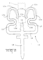
- Each terminal 10 has opposed beams 12 extending upwardly from a base 14.
- a post or barb 16 extends upwardly from the center of the base 14 between the opposed beams.
- a contact tail 18, aligned with the post or barb 16 extends from the bottom of the base and is suitable for establishing an electrical interconnection with a printed circuit board on which the socket 2 can be mounted.
- the opposed beams 12 are deflectable upon insertion of a circuit panel 4 between the beams.
- Each of the beams 12 comprises an upwardly extending portion, extending from one end of the base 14 which extends between the two opposed beams 12.
- the upwardly extending portion 12a is connected to the base 14 and is inclined inwardly.
- Inwardly inclined arms 12b extend downwardly from the top 12c of the upwardly extending portion. These inwardly inclined arms 12b diverge from the inwardly inclined portion of the upwardly extending portion 12a.
- An inwardly extending loop section 12d is located between the top and the bottom of the upwardly extending portion 12a of each of the opposed beams 12.
- the elevation of inwardly extending loop section 12d is such that it is located between the base 14 and the end of the downwardly extending portion 12b. Indeed, the inwardly extending loop 12d is located below the downwardly extending portion 12b in the preferred embodiment of this invention.
- the inwardly extending loop section 12d is a generally U shaped member in which the bight of the loop section 12c is located along the inner edge of the opposed beams 12 with the open portion of the U-shaped loop facing outward.
- the two parallel sides of the U shaped loop section 12c are generally parallel to the base 14 and the bight is generally curved.
- a contact point 12e is located at the innermost extent of the downwardly extending portion 12b and the contact point 12e is located adjacent the end of each beam 12.
- the contact 12e is located above the loop section 12d.
- the opposed beams 12 are configured such that the majority of the flexure of the opposed beams 12 in the loop section 12d, the base 14 and in that portion of the terminal between the base and the loop. A relatively large deflection of the contact point 12e can be achieved without increasing the height of the beams 12.
- Post 16 which comprises a barb, extends upwardly from the base 14 between the two opposed beams 12. Indeed, post 16 is located between the two contact points 12e on opposed beams 12. The elevation of the upper surface of post 16 is such that it is substantially at the same elevation as the loop section 12c.
- the insulative housing 20 can be molded of conventional engineering plastic materials suitable for use in electrical connectors.
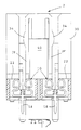
- Housing 20 has a generally rectangular central section extending between two panel guide or panel support members 30 located at either end thereof.
- two panel receiving slots 20 extend between the panel guides 30 and open upwardly on the upper face 20a in the insulative housing 20.
- the two slots 22 are parallel.
- a plurality of cavities 24 also open upwardly on the upper face 20a of the insulative housing 20 and communicate with a corresponding panel receiving slot 22 in the dual row connector comprising the preferred embodiment of the invention. Individual cavities 24 communicate only with one of the slots 22.
- Each of the cavities 24 is open on the top and the bottom of the insulative housing 20 and each cavity 24 extends on opposite sides of the corresponding upwardly open slot 22.
- a central spine 26 comprises the portion of the insulative housing 20 located below each of the panel receiving slots 22. As shown in Figure 5, the central spine 26 comprises a solid portion of the insulative housing 20 at positions between cavities 24. The cavities 24 are positioned to intersect the slot 22 with housing ribs 28 comprising that portion of the central spine 26 extending through each cavity. These housing ribs 28 extend downwardly from the lower surface of slots 22, which comprises the upper surface of the central spine 26, and a hole 26a is located between the housing ribs 28. Each cavity 24 is open both on the upper face 20a of the insulative housing and on the lower face 20b. Each cavity 24 extends below the housing ribs 28.
- the panel guide or panel support members 32 are located at the opposite ends of the insulative housing 20. Each of these panel guides extends upwardly above the upper face 20a of the insulative housing 20 and has an inner face 30a. Panel grooves 32 having open inner ends are inwardly facing and communicate with each panel receiving slot 20. Panel grooves 32 also extend upwardly above the panel receiving slots 22. Panel gripping portions in the form of ridges 34 which comprise constricted portions of the panel receiving grooves 32 are spaced above the open upper end of the panel receiving slot 22. Recesses or relief slots 36 are located on opposite sides of the grooves 32 to define flexible walls 38. These flexible walls are joined as part of the panel support members 30 in the preferred embodiment of this invention. A central pocket 40 is located along the lower end of the panel support members 30 in the preferred embodiment of this invention, and the relief slots 36 in the vicinity of ridges 34 extend upwardly from this pocket 40.
- Terminals 10 are inserted into corresponding cavities 24 from the bottom of the insulative housing 20.
- the contact points 12e of the opposed beam 12 are spaced apart by a distance less than the width of the central spine within the cavities. In other words, the contact points 12e are spaced apart by a distance less than the spacing of the exterior surfaces of the two ribs 28 within the cavities 26.
- the opposed beams 12 are deflected outwardly upon engagement with the ribs 28.
- the inwardly inclined arms to spring back to their original position so that each inwardly inclined arm 12b projects into the slot from opposite sides. In other words, the contact point 12e is now positioned within the panel receiving slot 22.
- the post or barb 16 extending upwardly from the base 14 on terminal 10 is also aligned with the panel receiving slot 22.
- the upper surface of each post 16 extends above the bottom of the cavity.
- the post or barb 16 extends into the hole 26a located between the two housing ribs 12b and the barb secures the corresponding terminal to the central spine 26 by virtue of its engagement with the two ribs 28.
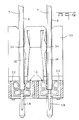
- the traces, or the contact pads located on the ends of the traces adjacent the edge 4a of the circuit panel engage the downwardly extending portion 12b of the opposed beams 12 and deflects these downwardly extending inwardly inclined arms 12b outwardly.
- Contact points 12e are brought into contact with these traces adjacent the edge 4a of the circuit panel.
- the edge 4a of the circuit panel is also juxtaposed to the post so that contact points indeed engage these traces adjacent the edge. Full force wiping between the contacts and trace pads occurs. Such engagement is especially significant when a non-standard single in-line memory module is employed in this socket.
- the panel support members 30 are also configured to support and stabilize especially tall single in-line memory modules. As the circuit panel is inserted into the grooves 32, aligned with the panel receiving slots 20, the flexible walls 38 are deflected when the ridges, forming a constricted portion 34, engage the sides of the circuit panel 4. These ridges serve to both align and secure the circuit panel within the socket 2.
- an alternate panel support guide configuration 130 can be employed with cantilever beams 138 having a panel gripping protrusion 134 adjacent their upper ends.
- Figure 7 therefore illustrates that terminals 10 can be employed in other configurations and are not dependant upon the use with the panel support guides 30 comprising the preferred embodiment of this invention. Therefore, it would be clear to one of ordinary skill in the art that the instant invention can be employed in differing configurations and the following claims are not limited to the precise embodiment depicted as the preferred embodiment of this invention or the embodiment comprising the alternate embodiment of Figure 7.
Landscapes
- Coupling Device And Connection With Printed Circuit (AREA)
- Multi-Conductor Connections (AREA)
- Connections Arranged To Contact A Plurality Of Conductors (AREA)
Applications Claiming Priority (2)
| Application Number | Priority Date | Filing Date | Title |
|---|---|---|---|
| US36064489A | 1989-06-02 | 1989-06-02 | |
| US360644 | 1989-06-02 |
Publications (3)
| Publication Number | Publication Date |
|---|---|
| EP0400378A2 true EP0400378A2 (de) | 1990-12-05 |
| EP0400378A3 EP0400378A3 (de) | 1991-02-06 |
| EP0400378B1 EP0400378B1 (de) | 1996-01-03 |
Family
ID=23418870
Family Applications (1)
| Application Number | Title | Priority Date | Filing Date |
|---|---|---|---|
| EP90108923A Expired - Lifetime EP0400378B1 (de) | 1989-06-02 | 1990-05-11 | Leiterplattensockel mit Kleeblattkontakt |
Country Status (7)
| Country | Link |
|---|---|
| EP (1) | EP0400378B1 (de) |
| JP (1) | JP2660450B2 (de) |
| KR (1) | KR100190795B1 (de) |
| CN (1) | CN1047941A (de) |
| AT (1) | ATE132661T1 (de) |
| DE (1) | DE69024535T2 (de) |
| ES (1) | ES2083395T3 (de) |
Cited By (8)
| Publication number | Priority date | Publication date | Assignee | Title |
|---|---|---|---|---|
| EP0554003A1 (de) * | 1992-01-31 | 1993-08-04 | The Whitaker Corporation | Beidseitig ausgestattete Verlängerungsfassung für Ausleseplatinen |
| EP0557898A1 (de) * | 1992-02-24 | 1993-09-01 | Molex Incorporated | Steckverbinder für die Kante einer gedruckten Schaltung |
| EP0564955A2 (de) * | 1992-04-06 | 1993-10-13 | Molex Incorporated | Randverbinder für eine Leiterplatte |
| EP0881679A2 (de) * | 1997-05-27 | 1998-12-02 | Fujitsu Limited | Halbleitermodul mit einer Mehrzahl von abtrennbaren Halbleiterbauteilen |
| US6733017B2 (en) | 2001-09-14 | 2004-05-11 | Air Systems, Inc. | Gas cylinder cart with removable control panel |
| USD822302S1 (en) | 2016-09-22 | 2018-07-03 | Air Systems, Inc. | Air cylinder cart frame |
| US10053124B2 (en) | 2016-09-22 | 2018-08-21 | Air Systems, Inc. | Air cylinder cart with manifold for supplying one or two control panels |
| USD854274S1 (en) | 2017-08-23 | 2019-07-16 | Air Systems, Inc. | Air cylinder cart frame |
Families Citing this family (3)
| Publication number | Priority date | Publication date | Assignee | Title |
|---|---|---|---|---|
| WO2011072199A2 (en) * | 2009-12-10 | 2011-06-16 | Surmodics, Inc. | Water-soluble degradable photo-crosslinker |
| CN109066152A (zh) * | 2018-08-24 | 2018-12-21 | 郑州云海信息技术有限公司 | 一种连接器 |
| CN109917164A (zh) * | 2019-04-10 | 2019-06-21 | 浙江正泰仪器仪表有限责任公司 | 电能表以及电能表表箱 |
Citations (3)
| Publication number | Priority date | Publication date | Assignee | Title |
|---|---|---|---|---|
| DE1812633A1 (de) * | 1968-12-04 | 1970-06-18 | Rohde & Schwarz | Kontaktleiste fuer gedruckte Schaltungsplatten |
| US4046444A (en) * | 1975-10-14 | 1977-09-06 | General Cable Corporation | Connector for use with printed wiring circuits |
| US4722700A (en) * | 1987-01-23 | 1988-02-02 | Amp Incorporated | Low insertion force terminal for use with circuit panel |
Family Cites Families (3)
| Publication number | Priority date | Publication date | Assignee | Title |
|---|---|---|---|---|
| JPS5322783Y2 (de) * | 1972-07-04 | 1978-06-13 | ||
| JPS5328070Y2 (de) * | 1972-07-05 | 1978-07-15 | ||
| EP0158413B1 (de) * | 1984-04-06 | 1990-01-31 | Molex Incorporated | Elektrischer Stecker mit geringer notwendiger Einsteckkraft und mit beanspruchungsüberwachten Kontakten |
-
1990
- 1990-05-11 AT AT90108923T patent/ATE132661T1/de not_active IP Right Cessation
- 1990-05-11 ES ES90108923T patent/ES2083395T3/es not_active Expired - Lifetime
- 1990-05-11 EP EP90108923A patent/EP0400378B1/de not_active Expired - Lifetime
- 1990-05-11 DE DE69024535T patent/DE69024535T2/de not_active Expired - Fee Related
- 1990-05-31 JP JP2140157A patent/JP2660450B2/ja not_active Expired - Lifetime
- 1990-06-01 CN CN90103972A patent/CN1047941A/zh active Pending
- 1990-06-01 KR KR1019900008082A patent/KR100190795B1/ko not_active IP Right Cessation
Patent Citations (3)
| Publication number | Priority date | Publication date | Assignee | Title |
|---|---|---|---|---|
| DE1812633A1 (de) * | 1968-12-04 | 1970-06-18 | Rohde & Schwarz | Kontaktleiste fuer gedruckte Schaltungsplatten |
| US4046444A (en) * | 1975-10-14 | 1977-09-06 | General Cable Corporation | Connector for use with printed wiring circuits |
| US4722700A (en) * | 1987-01-23 | 1988-02-02 | Amp Incorporated | Low insertion force terminal for use with circuit panel |
Cited By (12)
| Publication number | Priority date | Publication date | Assignee | Title |
|---|---|---|---|---|
| EP0554003A1 (de) * | 1992-01-31 | 1993-08-04 | The Whitaker Corporation | Beidseitig ausgestattete Verlängerungsfassung für Ausleseplatinen |
| EP0557898A1 (de) * | 1992-02-24 | 1993-09-01 | Molex Incorporated | Steckverbinder für die Kante einer gedruckten Schaltung |
| EP0564955A2 (de) * | 1992-04-06 | 1993-10-13 | Molex Incorporated | Randverbinder für eine Leiterplatte |
| EP0564955A3 (en) * | 1992-04-06 | 1996-03-13 | Molex Inc | Edge connector for a printed circuit board |
| EP0881679A2 (de) * | 1997-05-27 | 1998-12-02 | Fujitsu Limited | Halbleitermodul mit einer Mehrzahl von abtrennbaren Halbleiterbauteilen |
| EP0881679A3 (de) * | 1997-05-27 | 2000-08-02 | Fujitsu Limited | Halbleitermodul mit einer Mehrzahl von abtrennbaren Halbleiterbauteilen |
| US6472744B2 (en) | 1997-05-27 | 2002-10-29 | Fujitsu Limited | Semiconductor module including a plurality of semiconductor devices detachably |
| US6696754B2 (en) | 1997-05-27 | 2004-02-24 | Fujitsu Limited | Semiconductor module including a plurality of semiconductor devices detachably |
| US6733017B2 (en) | 2001-09-14 | 2004-05-11 | Air Systems, Inc. | Gas cylinder cart with removable control panel |
| USD822302S1 (en) | 2016-09-22 | 2018-07-03 | Air Systems, Inc. | Air cylinder cart frame |
| US10053124B2 (en) | 2016-09-22 | 2018-08-21 | Air Systems, Inc. | Air cylinder cart with manifold for supplying one or two control panels |
| USD854274S1 (en) | 2017-08-23 | 2019-07-16 | Air Systems, Inc. | Air cylinder cart frame |
Also Published As
| Publication number | Publication date |
|---|---|
| ATE132661T1 (de) | 1996-01-15 |
| EP0400378B1 (de) | 1996-01-03 |
| ES2083395T3 (es) | 1996-04-16 |
| EP0400378A3 (de) | 1991-02-06 |
| CN1047941A (zh) | 1990-12-19 |
| JPH0322380A (ja) | 1991-01-30 |
| DE69024535T2 (de) | 1996-05-15 |
| KR910002047A (ko) | 1991-01-31 |
| JP2660450B2 (ja) | 1997-10-08 |
| KR100190795B1 (ko) | 1999-06-01 |
| DE69024535D1 (de) | 1996-02-15 |
Similar Documents
| Publication | Publication Date | Title |
|---|---|---|
| US4973270A (en) | Circuit panel socket with cloverleaf contact | |
| EP0416322B1 (de) | Kontaktendstück in einem Schaltplattensockel | |
| US4990097A (en) | Electrical connector with module extraction apparatus | |
| JP4955731B2 (ja) | 基板対基板電気コネクタ組立体 | |
| US5188535A (en) | Low profile electrical connector | |
| US5876217A (en) | Electric connector assembly with improved retention characteristics | |
| US4986765A (en) | Insertable latch means for use in an electrical connector | |
| US7748994B1 (en) | Board-to-board connector assembly | |
| US4708415A (en) | Electrical connectors | |
| US6729890B2 (en) | Reduced-size board-to-board connector | |
| US5046972A (en) | Low insertion force connector and contact | |
| US5145386A (en) | Low profile electrical connector | |
| US5046955A (en) | Active connector assembly | |
| EP0499378A2 (de) | Flachprofil-nockenbetätigte Simm-Buchse | |
| EP0356156A2 (de) | Randverbinder für Leiterplatten und Anschlusselement dafür | |
| EP0645852A2 (de) | Leiterplattenbefestigung eines elektrischen Verbinders | |
| US5004434A (en) | Printed circuit board edge connector | |
| US5254017A (en) | Terminal for low profile edge socket | |
| US4722700A (en) | Low insertion force terminal for use with circuit panel | |
| US5219295A (en) | Electrical connector with guide member | |
| EP0717468A2 (de) | Zuerst Polkontakte zuletzt Erdkontakt unterbrechender Steckverbinder | |
| US4725250A (en) | High density circuit panel socket | |
| US5131872A (en) | Contact spring socket | |
| EP0400378B1 (de) | Leiterplattensockel mit Kleeblattkontakt | |
| IE78012B1 (en) | Electrical connector assembly for mounting on a printed circuit board |
Legal Events
| Date | Code | Title | Description |
|---|---|---|---|
| PUAI | Public reference made under article 153(3) epc to a published international application that has entered the european phase |
Free format text: ORIGINAL CODE: 0009012 |
|
| AK | Designated contracting states |
Kind code of ref document: A2 Designated state(s): AT BE CH DE ES FR GB IT LI LU NL |
|
| PUAL | Search report despatched |
Free format text: ORIGINAL CODE: 0009013 |
|
| AK | Designated contracting states |
Kind code of ref document: A3 Designated state(s): AT BE CH DE ES FR GB IT LI LU NL |
|
| 17P | Request for examination filed |
Effective date: 19901220 |
|
| RAP1 | Party data changed (applicant data changed or rights of an application transferred) |
Owner name: THE WHITAKER CORPORATION |
|
| 17Q | First examination report despatched |
Effective date: 19931027 |
|
| GRAA | (expected) grant |
Free format text: ORIGINAL CODE: 0009210 |
|
| AK | Designated contracting states |
Kind code of ref document: B1 Designated state(s): AT BE CH DE ES FR GB IT LI LU NL |
|
| REF | Corresponds to: |
Ref document number: 132661 Country of ref document: AT Date of ref document: 19960115 Kind code of ref document: T |
|
| ITF | It: translation for a ep patent filed | ||
| REF | Corresponds to: |
Ref document number: 69024535 Country of ref document: DE Date of ref document: 19960215 |
|
| ET | Fr: translation filed | ||
| REG | Reference to a national code |
Ref country code: ES Ref legal event code: FG2A Ref document number: 2083395 Country of ref document: ES Kind code of ref document: T3 |
|
| PG25 | Lapsed in a contracting state [announced via postgrant information from national office to epo] |
Ref country code: LU Free format text: LAPSE BECAUSE OF NON-PAYMENT OF DUE FEES Effective date: 19960531 |
|
| PLBE | No opposition filed within time limit |
Free format text: ORIGINAL CODE: 0009261 |
|
| STAA | Information on the status of an ep patent application or granted ep patent |
Free format text: STATUS: NO OPPOSITION FILED WITHIN TIME LIMIT |
|
| 26N | No opposition filed | ||
| PGFP | Annual fee paid to national office [announced via postgrant information from national office to epo] |
Ref country code: ES Payment date: 19980522 Year of fee payment: 9 |
|
| PGFP | Annual fee paid to national office [announced via postgrant information from national office to epo] |
Ref country code: BE Payment date: 19980609 Year of fee payment: 9 |
|
| PGFP | Annual fee paid to national office [announced via postgrant information from national office to epo] |
Ref country code: CH Payment date: 19980709 Year of fee payment: 9 |
|
| PGFP | Annual fee paid to national office [announced via postgrant information from national office to epo] |
Ref country code: NL Payment date: 19990322 Year of fee payment: 10 |
|
| PGFP | Annual fee paid to national office [announced via postgrant information from national office to epo] |
Ref country code: AT Payment date: 19990406 Year of fee payment: 10 |
|
| PGFP | Annual fee paid to national office [announced via postgrant information from national office to epo] |
Ref country code: FR Payment date: 19990504 Year of fee payment: 10 |
|
| PG25 | Lapsed in a contracting state [announced via postgrant information from national office to epo] |
Ref country code: ES Free format text: THE PATENT HAS BEEN ANNULLED BY A DECISION OF A NATIONAL AUTHORITY Effective date: 19990512 |
|
| PG25 | Lapsed in a contracting state [announced via postgrant information from national office to epo] |
Ref country code: LI Free format text: LAPSE BECAUSE OF NON-PAYMENT OF DUE FEES Effective date: 19990531 Ref country code: CH Free format text: LAPSE BECAUSE OF NON-PAYMENT OF DUE FEES Effective date: 19990531 Ref country code: BE Free format text: LAPSE BECAUSE OF NON-PAYMENT OF DUE FEES Effective date: 19990531 |
|
| PGFP | Annual fee paid to national office [announced via postgrant information from national office to epo] |
Ref country code: DE Payment date: 19990531 Year of fee payment: 10 |
|
| BERE | Be: lapsed |
Owner name: THE WHITAKER CORP. Effective date: 19990531 |
|
| PGFP | Annual fee paid to national office [announced via postgrant information from national office to epo] |
Ref country code: GB Payment date: 20000404 Year of fee payment: 11 |
|
| PG25 | Lapsed in a contracting state [announced via postgrant information from national office to epo] |
Ref country code: AT Free format text: LAPSE BECAUSE OF NON-PAYMENT OF DUE FEES Effective date: 20000511 |
|
| PG25 | Lapsed in a contracting state [announced via postgrant information from national office to epo] |
Ref country code: NL Free format text: LAPSE BECAUSE OF NON-PAYMENT OF DUE FEES Effective date: 20001201 |
|
| PG25 | Lapsed in a contracting state [announced via postgrant information from national office to epo] |
Ref country code: FR Free format text: LAPSE BECAUSE OF NON-PAYMENT OF DUE FEES Effective date: 20010131 |
|
| NLV4 | Nl: lapsed or anulled due to non-payment of the annual fee |
Effective date: 20001201 |
|
| PG25 | Lapsed in a contracting state [announced via postgrant information from national office to epo] |
Ref country code: DE Free format text: LAPSE BECAUSE OF NON-PAYMENT OF DUE FEES Effective date: 20010301 |
|
| REG | Reference to a national code |
Ref country code: FR Ref legal event code: ST |
|
| PG25 | Lapsed in a contracting state [announced via postgrant information from national office to epo] |
Ref country code: GB Free format text: LAPSE BECAUSE OF NON-PAYMENT OF DUE FEES Effective date: 20010511 |
|
| GBPC | Gb: european patent ceased through non-payment of renewal fee |
Effective date: 20010511 |
|
| REG | Reference to a national code |
Ref country code: ES Ref legal event code: FD2A Effective date: 20020204 |
|
| PG25 | Lapsed in a contracting state [announced via postgrant information from national office to epo] |
Ref country code: IT Free format text: LAPSE BECAUSE OF NON-PAYMENT OF DUE FEES;WARNING: LAPSES OF ITALIAN PATENTS WITH EFFECTIVE DATE BEFORE 2007 MAY HAVE OCCURRED AT ANY TIME BEFORE 2007. THE CORRECT EFFECTIVE DATE MAY BE DIFFERENT FROM THE ONE RECORDED. Effective date: 20050511 |
|
| REG | Reference to a national code |
Ref country code: CH Ref legal event code: PL Ref country code: CH Ref legal event code: NV Representative=s name: DR. CONRAD A. RIEDERER PATENTANWALT Ref country code: CH Ref legal event code: EP |