EP0399362B1 - A sense amplifier circuit - Google Patents
A sense amplifier circuit Download PDFInfo
- Publication number
- EP0399362B1 EP0399362B1 EP90109264A EP90109264A EP0399362B1 EP 0399362 B1 EP0399362 B1 EP 0399362B1 EP 90109264 A EP90109264 A EP 90109264A EP 90109264 A EP90109264 A EP 90109264A EP 0399362 B1 EP0399362 B1 EP 0399362B1
- Authority
- EP
- European Patent Office
- Prior art keywords
- bit line
- excess charge
- transistor
- sense amplifier
- voltage
- Prior art date
- Legal status (The legal status is an assumption and is not a legal conclusion. Google has not performed a legal analysis and makes no representation as to the accuracy of the status listed.)
- Expired - Lifetime
Links
Images


Classifications
-
- G—PHYSICS
- G11—INFORMATION STORAGE
- G11C—STATIC STORES
- G11C16/00—Erasable programmable read-only memories
- G11C16/02—Erasable programmable read-only memories electrically programmable
- G11C16/06—Auxiliary circuits, e.g. for writing into memory
-
- G—PHYSICS
- G11—INFORMATION STORAGE
- G11C—STATIC STORES
- G11C7/00—Arrangements for writing information into, or reading information out from, a digital store
- G11C7/06—Sense amplifiers; Associated circuits, e.g. timing or triggering circuits
- G11C7/067—Single-ended amplifiers
-
- G—PHYSICS
- G11—INFORMATION STORAGE
- G11C—STATIC STORES
- G11C16/00—Erasable programmable read-only memories
- G11C16/02—Erasable programmable read-only memories electrically programmable
- G11C16/06—Auxiliary circuits, e.g. for writing into memory
- G11C16/26—Sensing or reading circuits; Data output circuits
-
- G—PHYSICS
- G11—INFORMATION STORAGE
- G11C—STATIC STORES
- G11C17/00—Read-only memories programmable only once; Semi-permanent stores, e.g. manually-replaceable information cards
- G11C17/08—Read-only memories programmable only once; Semi-permanent stores, e.g. manually-replaceable information cards using semiconductor devices, e.g. bipolar elements
- G11C17/10—Read-only memories programmable only once; Semi-permanent stores, e.g. manually-replaceable information cards using semiconductor devices, e.g. bipolar elements in which contents are determined during manufacturing by a predetermined arrangement of coupling elements, e.g. mask-programmable ROM
- G11C17/12—Read-only memories programmable only once; Semi-permanent stores, e.g. manually-replaceable information cards using semiconductor devices, e.g. bipolar elements in which contents are determined during manufacturing by a predetermined arrangement of coupling elements, e.g. mask-programmable ROM using field-effect devices
-
- G—PHYSICS
- G11—INFORMATION STORAGE
- G11C—STATIC STORES
- G11C7/00—Arrangements for writing information into, or reading information out from, a digital store
- G11C7/12—Bit line control circuits, e.g. drivers, boosters, pull-up circuits, pull-down circuits, precharging circuits, equalising circuits, for bit lines
Definitions
- the present invention relates to a sense amplifier circuit for a reading circuit of a semiconductor memory apparatus, and more particularly to a sense amplifier circuit for a read only memory.
- Recent non-volatile memories such as read-only memories (called ROM hereinafter) are required to have large capacity and to operate at high speed.
- ROM read-only memories
- the memory cell area must be decreased, even if this requires that the current-driving ability of the memory cell transistor be decreased.
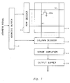
- a ROM is formed as shown in Figure 1.
- 10 is a memory cell array comprising a plurality of word lines WL and bit lines BL, and a memory cell 10a provided at respective crossing portions of these word lines WL and bit lines BL.
- Memory cell 10a comprises, for example, a MOS transistor whose gate is connected to word line WL and whose drain is connected to bit line BL.
- Memory cell 10a may comprise a bipolar transistor.
- Word lines WL are selected by row decoder 11 and bit lines BL are selected by column decoder 12, and an address signal is input to these row and column decoders through address buffer 13.
- the read output of a bit line BL selected by the column decoder 12 is amplified by sense amplifier 14 and is outputted externally through output buffer 15.
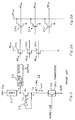
- Fig. 2 shows the general constitution of a known sense amplifier circuit.
- a sense amplifier circuit comprises a serial connection of a load 21, a transistor 21 and a memory cell 20, being connected between a power source V CC and ground GND.
- Memory cell 20 comprises a plurality of memory cells 20a, 20b.... as shown in Figures 3A and 3B.
- Figure 3A designates a serial type memory cell
- Figure 3B designates a parallel type memory cell.
- memory cells 20a, 20b... which are formed of transistors, store either "1 " or "0” depending on whether the transistor is of an enhancement type or of a depletion type.
- "1" or "0" is stored depending on whether the threshold value is high or low.
- the non-selection word line is made to level H and the selection word line is made to level L.
- the word line WLb is selected, other word lines WLa, WLc, ... are at H level and transistors 20a, 20c... are on regardless of whether the stored value is "1" or "0". Only transistor 20b, belonging to the selected word line, is turned on and off, depending on whether 1 or 0 is stored. If transistor 20b is of the depletion type it is on and if it is of the enhancement type it is off.
- the data stored in memory cell 20b is determined to be 1 or 0, and thus a current flows or does not flow in bit line BLa.
- the potential V C at the connecting point between load 21 and transistor Q1 in Figure 2 changes depending on whether or not the bit line current (i cel ) flows and voltage output circuit 22 detects potential V C and produces read out data.
- the selected word line is at H level and the non-selected word line is at L level. Accordingly, memory cells belonging to non-selected word lines are turned off regardless of whether "1" or “0” is stored, and only the memory cell belonging to the selected word line is turned on or off depending on whether “1” or “0” is stored. A current flows or does not flow in bit line BLa, depending on whether the memory cell is turned on or off, thereby changing the voltage V C . Voltage output circuit 22 then detects the voltage V C and produces the read-out data. Voltage output circuit 22 basically comprises only a line, but may be formed of a circuit for driving an output side circuit to be connected to the sense amplifier.
- a column selection gate which is turned on or off depending on the output of decoder 12, is provided between transistor Q1 and the bit line (cell group).
- the variation of the bit line voltage v a is suppressed, whether the bit line current I CEL is turned on or off.
- the voltage V C is equal to VCC-Rx icel under the condition that the resistance of load 21 is R and changes as shown in the drawing, depending on whether the cell is switched on or off.
- Figures 4A to 4H Various kinds of inverters 23 are shown in Figures 4A to 4H.
- Figure 4A shows an E-D type
- Figure 4B an E-E type
- Figure 4C and Figure 4D CMOS types in which Qa is an n-channel enhancement type MOS transistor, Qb is an n-channel depletion type MOS transistor and Qd is a p-channel type MOS transistor.
- Figures 4E to 4H show only load portions.
- the gate of p-channel type transistor Qd is connected to ground in Figures 4C and 4G, connected to input IN in Figure 4D and connected to the drain (output OUT) in Figure 4H.
- the input-output characteristic of inverter 23 is shown in Figure 6.
- the current is divided into several steps and for binary-value logic, the two states, i.e., the state in which current flows and the state in which current does not flow, are provided. Let us explain the example of two steps in which the current flows or does not flow.
- the output of inverter 23 is fed back to the input of inverter 23 through transistor Q1.
- the input-output characteristic of the inverter is abrupt. Therefore, the range of variation of v a can be made small, and v b can be changed quickly. That is, the variation of V a is made small so that the existence of a bit line capacitance shown in Figure 7 does not greatly affect the operation of the cell 20, and the range of the variation in v b is made large, thus enabling the on/off control of transistor Q1 to be conducted at high speed and with certainty.
- a column selection gate shown in Figure 7 is connected between a cell 20 and a sense amplifier comprising transistor Q1, inverter 23 and load 21 and has a relatively large capacitance.
- a parasitic capacitance C WB exists between bit line BL and word line WL.
- C BL is a parasitic capacitance existing between bit line BL and ground.
- the bit line potential is almost equal to v a .
- a change in v a means that the bit line potential changes and that the charges stored in bit line capacitances C BL and C WB change accordingly.
- the sense amplifier operates only after the excess charge is discharged by the cell transistor.
- the reason for the above operation is that a variation in word line potential is reflected on a bit line by a parasitic capacitance C WB between a word line and a bit line and that an operation point of a sense amplifier varies in accordance with a power source potential variation caused by a noise.
- v a increases and v b decreases, thereby providing a new stable state under the voltage V CC + ⁇ V (state C, b ⁇ c).
- V CC voltage + ⁇ V
- a time delay or a surplus time period shown in a state F′ and d ⁇ a time delay is relatively unimportant, but when the current driving capability of the cell, i.e., the current driving capability by which the input-output characteristic is driven from d to e, becomes weak because of a fine pattern of the cell, the time delay in this surplus time period F′ becomes large, greatly affecting access time.
- An object of the present invention is to make improvements regarding the above points and, by preventing excess charge-up of bit line capacitance, to realize a sense amplifier with high speed operation.
- a feature of the present invention resides in a sense amplifier circuit for use in a non-volatile memory comprising, an excess charge detecting circuit for producing a detection output when the potential of a bit line exceeds a normal value, an excess charge discharging circuit which operates in response to said excess charge detecting circuit for discharging a bit line charge and for returning the bit line potential to the normal value.
- the present invention provides a circuit 24 for detecting an excess charge up of a bit line and an excess charge discharging circuit 25 to be operated by the output of detecting circuit 24.
- excess charge up can be detected as an increase in potential.
- excess charge detecting circuit 24 receives a bit line potential v a and detects the excess charge up.
- excess charge detecting circuit 24 receives the output voltage v b (a gate voltage of transistor Q1) from inverter 23 and, as shown in Figure 11D, receives both voltages v a and v b .
- excess charge discharging circuit 25 operates to discharge the excess bit line charge.
- bit line potential decreases, deviating from the excess charge up state, and discharging circuit 25 stops the operation.
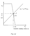
- the excess charge detecting circuit of Figures 11A, 11B and 11C detects an abnormality of v a , v b , and v b - v a .
- excess charge detecting circuit 24 comprises voltage judging circuit 24a for judging the voltage v a and excess charge discharging circuit 25 comprises a transistor 25a connected between the bit line and ground.
- An inverter shown in Figure 4A to 4H or comparator CMP shown in Figure 13C can be used for voltage judging circuit 24a.
- the inverter detects an excess charge based on whether or not the voltage v a exceeds a threshold value and the comparator detects the excess charge based on whether or not the voltage v a exceeds a reference voltage REF.
- the output of voltage judging circuit 24a becomes H level and transistor 25a is turned ON, thereby discharging the bit line charge.
- the output of voltage judging circuit 24a becomes L and transistor 25a is turned OFF, thereby stopping the discharge.
- voltage judging circuit 24a observes the output of the inverter and transistor 25a turns ON when the inverter output v b decreases and becomes less than the threshold value or the reference voltage.
- Figures 14A and 14B are similar to Figures 13A and 13B.
- n-channel transistor 25a is used but in Figures 14A and 14B, p-channel transistor 25b is used. Except for this feature, Figures 14A and 14B are the same as Figures 13A and 13B.
- excess charge detecting circuit 24 and excess charge discharging circuit 25 are formed of a single transistor 25c.
- This transistor 25c is diode-connected and the threshold value is determined as V th2 .
- transistor 25c turns ON, thereby discharging the charge.
- This state is shown in Figure 15A. Although the correction is lacking by P1 - P as compared with a normal state, the circuit is made simple.
- excess charge detecting circuit 24 and excess charge discharging circuit 25 are formed of n-channel transistor 24b, 24c and 25d.
- the voltage at the serial connecting point between transistors 24b and 24c is determined as V d .
- transistor 25d turns ON and transistor 25c is normally ON, thereby discharging the excess bit-line charge.
- V d is smaller than v b by the threshold value V th3 of transistor 24b and thus, point P1 is made closer to point P than in Figure 14C.
- excess charge detecting circuit 24 is formed of n-channel MOS transistors 24b, 24d and 24c and excess charge discharging circuit 25 is formed of p-channel transistor 25b.
- transistor 25b when transistor 25b is determined to have threshold value v th2 , and then v a - v d ⁇ V th2 , transistor 25b turns ON, thereby discharging the bit-line excess charge.
- v a1 - v a0 (V thN - V thp )/(1 + A)
- v b0 - v b1 A(V thN - V thp )/(1 + A) ⁇ V thN - V thp
- VthN ⁇ Vthp (generally speaking, the difference is about 100mV), Va1 ⁇ Vao and Vpo ⁇ Vp1.
- the present invention can prevent the bit line potential from being charged up to more than the predetermined value and can decrease the sense time delay caused by an excess charge-discharge and further can sense the data at high speed even for a cell with a weak current driving capability, thereby contributing to the high density of the integration.
Landscapes
- Read Only Memory (AREA)
- Semiconductor Memories (AREA)
Description
- The present invention relates to a sense amplifier circuit for a reading circuit of a semiconductor memory apparatus, and more particularly to a sense amplifier circuit for a read only memory.
- Recent non-volatile memories such as read-only memories (called ROM hereinafter) are required to have large capacity and to operate at high speed. In order to realize a large memory capacity, the memory cell area must be decreased, even if this requires that the current-driving ability of the memory cell transistor be decreased. Thus, it is necessary to develop a sense amplifier which operates at a small cell current.
- A ROM is formed as shown in Figure 1. 10 is a memory cell array comprising a plurality of word lines WL and bit lines BL, and a
memory cell 10a provided at respective crossing portions of these word lines WL and bit lines BL.Memory cell 10a comprises, for example, a MOS transistor whose gate is connected to word line WL and whose drain is connected to bit line BL.Memory cell 10a may comprise a bipolar transistor. Word lines WL are selected by row decoder 11 and bit lines BL are selected by column decoder 12, and an address signal is input to these row and column decoders throughaddress buffer 13. The read output of a bit line BL selected by the column decoder 12 is amplified by sense amplifier 14 and is outputted externally through output buffer 15. - Fig. 2 shows the general constitution of a known sense amplifier circuit. As shown in Fig. 2, such a sense amplifier circuit comprises a serial connection of a
load 21, atransistor 21 and amemory cell 20, being connected between a power source VCC and ground GND. - A potential at the crossing point of
load 21 and transistor Q₁ is detected byvoltage output circuit 22. The source potential va of transistor Q₁ is inverted byinverter 23 and applied to a gate of transistor Q₁.Memory cell 20 comprises a plurality ofmemory cells 20a, 20b.... as shown in Figures 3A and 3B. Figure 3A designates a serial type memory cell and Figure 3B designates a parallel type memory cell. In a serial type memory,memory cells 20a, 20b..., which are formed of transistors, store either "1 " or "0" depending on whether the transistor is of an enhancement type or of a depletion type. In a parallel type memory, "1" or "0" is stored depending on whether the threshold value is high or low. - In the configuration of Figure 3A, the non-selection word line is made to level H and the selection word line is made to level L. When the word line WLb is selected, other word lines WLa, WLc, ... are at H level and transistors 20a, 20c... are on regardless of whether the stored value is "1" or "0". Only
transistor 20b, belonging to the selected word line, is turned on and off, depending on whether 1 or 0 is stored. Iftransistor 20b is of the depletion type it is on and if it is of the enhancement type it is off. Accordingly, depending on whethermemory cell 20b is of the depletion type or the enhancement type, the data stored inmemory cell 20b is determined to be 1 or 0, and thus a current flows or does not flow in bit line BLa. The potential VC at the connecting point betweenload 21 and transistor Q₁ in Figure 2 changes depending on whether or not the bit line current (icel) flows andvoltage output circuit 22 detects potential VC and produces read out data. - In the configuration of Figure 3B, the selected word line is at H level and the non-selected word line is at L level. Accordingly, memory cells belonging to non-selected word lines are turned off regardless of whether "1" or "0" is stored, and only the memory cell belonging to the selected word line is turned on or off depending on whether "1" or "0" is stored. A current flows or does not flow in bit line BLa, depending on whether the memory cell is turned on or off, thereby changing the voltage VC.
Voltage output circuit 22 then detects the voltage VC and produces the read-out data.Voltage output circuit 22 basically comprises only a line, but may be formed of a circuit for driving an output side circuit to be connected to the sense amplifier. - A column selection gate, which is turned on or off depending on the output of decoder 12, is provided between transistor Q₁ and the bit line (cell group).
- By making the slope of the input-output characteristic abrupt when inverter 23 in a transient state, the variation of the bit line voltage va is suppressed, whether the bit line current ICEL is turned on or off. As shown in Figure 5, when the cell is on, i.e., when the bit-line current flows, the voltage va decreases, but the output vb of
inverter 23 increases. When the cell is off, the voltage Va increases but the output Vb ofinverter 23 decreases quickly, thus decreasing the width of the variation of the voltage va. This is effective for high speed operation. The voltage VC is equal to VCC-Rxicel under the condition that the resistance ofload 21 is R and changes as shown in the drawing, depending on whether the cell is switched on or off. - Various kinds of
inverters 23 are shown in Figures 4A to 4H. Figure 4A shows an E-D type, Figure 4B an E-E type, Figure 4C and Figure 4D CMOS types in which Qa is an n-channel enhancement type MOS transistor, Qb is an n-channel depletion type MOS transistor and Qd is a p-channel type MOS transistor. Figures 4E to 4H show only load portions. The gate of p-channel type transistor Qd is connected to ground in Figures 4C and 4G, connected to input IN in Figure 4D and connected to the drain (output OUT) in Figure 4H. The input-output characteristic ofinverter 23 is shown in Figure 6. When the input voltage va is L (low), the output voltage vb is H (high), and when the input voltage va is H (high), the output voltage vb is L (low). The input and the output characteristic changes proportionally between the above two states, as shown in Figure 6. The variation width Δva of the voltage va in Figure 6 is obtained from this proportionate area. Thus, the variation Δvb, which is expanded from the variation width Δva, can be obtained. The boundary at which the transistor Q₁ is turned on/off, is determined from vb - va = Vth1, assuming that Vth1 is the threshold voltage of the transistor. P1 is a balance point at which the cell is turned off and P2 is the balance point when the cell is tuned on. The variation of voltage va is small, as shown in Figure 6. - For multi-value logic, the current is divided into several steps and for binary-value logic, the two states, i.e., the state in which current flows and the state in which current does not flow, are provided. Let us explain the example of two steps in which the current flows or does not flow.
- As described above, the output of
inverter 23 is fed back to the input ofinverter 23 through transistor Q₁. Moreover, the input-output characteristic of the inverter is abrupt. Therefore, the range of variation of va can be made small, and vb can be changed quickly. That is, the variation of Va is made small so that the existence of a bit line capacitance shown in Figure 7 does not greatly affect the operation of thecell 20, and the range of the variation in vb is made large, thus enabling the on/off control of transistor Q₁ to be conducted at high speed and with certainty. When the memory cell is changed from a state in which current flows to a state in which current does not flow, the current stops flowing when vb -va is equal to the Vth of Q₁ (at point P₁). When a current flows in the memory cell, a charging operation of thebit line capacitance 24 is conducted and then completed. Thus, a current flowing through the bit line capacitance of the bit line is made 0. Thus, vb -va changes until the current flowing into transistor Q₁ becomes equal to the cell current (P₂). - A column selection gate shown in Figure 7 is connected between a
cell 20 and a sense amplifier comprising transistor Q1,inverter 23 andload 21 and has a relatively large capacitance. As shown in Figure 8, a parasitic capacitance CWB exists between bit line BL and word line WL. CBL is a parasitic capacitance existing between bit line BL and ground. The bit line potential is almost equal to va. Thus, a change in va means that the bit line potential changes and that the charges stored in bit line capacitances CBL and CWB change accordingly. When a current flows in thecell 20, thecell 20 has caused a discharge current of the bit line capacitance to flow, in addition to a sense current. The current flowing in thecell 20 and the sensed current differ in accordance with the amount of the discharge current. This is a factor contributing to access delay. - The fact that the change in va is small means that the change in bit line potential is small and thus that the change in charge stored in the bit line is small, thereby decreasing the delay in access speed caused by the discharge current and providing an advantage of increased operation speed.
- However, when the bit line potential exceeds that required for normal operation, the sense amplifier operates only after the excess charge is discharged by the cell transistor.
- The reason for the above operation is that a variation in word line potential is reflected on a bit line by a parasitic capacitance CWB between a word line and a bit line and that an operation point of a sense amplifier varies in accordance with a power source potential variation caused by a noise.
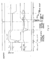
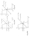
- Excess charge-up due to the power source voltage variation is explained by referring to Figures 9 and 10. The power source voltage is changed from an ordinary state (state A in Figure 9) of a cell off-state at the power source voltage VCC to a state at power source voltage VCC + ΔV. The input voltage va of
inverter 23 is detected under a new power source voltage Vcc+ΔV as if it would apparently decrease, thereby increasing vb (state B in Figure 9, a→b in Figure 10). As a result, current flows through transistor Q₁ and the bit line capacitance is charged up. As a result, va increases and vb decreases, thereby providing a new stable state under the voltage VCC + ΔV (state C, b→c). When the source voltage is returned from this state to VCC, it is detected as if va had increased and vb had decreased (state D, c→d). However, even if vb decreases by a large amount, transistor Q₁ only turns off at a voltage of less than vb - va = Vth1 and the current supply is cut off. Therefore, va maintains the present potential by means of a bit line capacitance (as shown by a dashed line in state E, d). When the state of the cell changes from OFF to ON as a result of an address selection by an addres signal ADDRESS, the excess charge is discharged through a cell transistor. The potential of va decreases and the potential of vb increases (as shown by a dashed line in state F′, d→a). After excess charge is discharged, until vb - va > Vth1, an ordinary sense operation is carried out (state G, a→e). In the conventional current driving capability of a cell transistor, a time delay or a surplus time period shown in a state F′ and d→a time delay is relatively unimportant, but when the current driving capability of the cell, i.e., the current driving capability by which the input-output characteristic is driven from d to e, becomes weak because of a fine pattern of the cell, the time delay in this surplus time period F′ becomes large, greatly affecting access time. - An object of the present invention is to make improvements regarding the above points and, by preventing excess charge-up of bit line capacitance, to realize a sense amplifier with high speed operation.
- This object is obtained as indicated in
claim 1. A feature of the present invention resides in a sense amplifier circuit for use in a non-volatile memory comprising, an excess charge detecting circuit for producing a detection output when the potential of a bit line exceeds a normal value, an excess charge discharging circuit which operates in response to said excess charge detecting circuit for discharging a bit line charge and for returning the bit line potential to the normal value. -
- Figure 1 shows a block diagram of a read only memory,
- Figure 2 shows an explanatory view of a sense amplifier circuit,
- Figures 3A and 3B show explanatory views of a memory cell array,
- Figures 4A to 4H show diagrams of circuits of various inverters,
- Figure 5 shows an explanatory view of an operation of a sense amplifier,
- Figure 6 shows an explanatory view of another operation of a sense amplifier,
- Figure 7 shows an explanatory view of a bit line parasitic capacitance,
- Figure 8 is a view for a explaining the capacitance between a word line and a bit line,
- Figure 9 is a view for explaining the operation where a power source voltage variation occurs by comparing a prior art device with the present invention,
- Figure 10 is a view for a explaining the operation where a power source voltage variation occurs,
- Figures 11A to 11D show views for explaining the principle of the present invention,
- Figure 12 shows an explanatory view of an excess charge state,
- Figures 13A and 13B and Figures 14A to 14E show circuits of various embodiments according to the present invention, and Figure 13C shows a comparator,
- Figures 15A to 15C show explanatory views of an operation of the embodiments shown in Figures 14A to 14E,
- As shown in Figure 11A, the present invention provides a
circuit 24 for detecting an excess charge up of a bit line and an excesscharge discharging circuit 25 to be operated by the output of detectingcircuit 24. - An excess charge up can be detected as an increase in potential. As shown in Figures 11A and 11B, excess
charge detecting circuit 24 receives a bit line potential va and detects the excess charge up. As shown in Figure 11C, excesscharge detecting circuit 24 receives the output voltage vb (a gate voltage of transistor Q₁) frominverter 23 and, as shown in Figure 11D, receives both voltages va and vb. - In this arrangement, when the excess charge of the bit line is detected by excess
charge detecting circuit 24, excesscharge discharging circuit 25 operates to discharge the excess bit line charge. Thus, the bit line potential decreases, deviating from the excess charge up state, and dischargingcircuit 25 stops the operation. - Therefore, the operation returns from d to a in Figure 10 and upon cell ON, a immediately moves to e, thereby starting a sensing operation. Thus, d is made close to e and a high speed operation is possible, by eliminating state F′ shown in Figure 9. In state E of Figure 9, because of the discharge of the excess bit line charge by excess
charge discharging circuit 25, Va decreases and thus Vb greatly increases, thereby decreasing the difference between Va and Vb, as shown by the solid line. Thus, in the present invention, surplus time period F is greatly shortened as compared with the prior art surplus time period F′. - The crossing point P between a straight line of vb -va = Vth1, and the input-output characteristic of the inverter is an ordinary point for the cell OFF, as shown in Figure 12. Ranges in which va is higher than this point P and in which vb is lower than this point P are considered to be within the excess charge state OC. The excess charge detecting circuit of Figures 11A, 11B and 11C detects an abnormality of va, vb, and vb - va.
- An embodiment of the present invention is shown in Figures 13A to 14D. The same parts are designated by the same reference numbers throughout all the drawings.
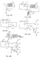
- In Figure 13A, excess
charge detecting circuit 24 comprises voltage judging circuit 24a for judging the voltage va and excesscharge discharging circuit 25 comprises atransistor 25a connected between the bit line and ground. An inverter shown in Figure 4A to 4H or comparator CMP shown in Figure 13C can be used for voltage judging circuit 24a. The inverter detects an excess charge based on whether or not the voltage va exceeds a threshold value and the comparator detects the excess charge based on whether or not the voltage va exceeds a reference voltage REF. When the bit line voltage va exceeds the threshold value or the reference voltage, the output of voltage judging circuit 24a becomes H level andtransistor 25a is turned ON, thereby discharging the bit line charge. When the bit line voltage va is decreased by this discharge operation, the output of voltage judging circuit 24a becomes L andtransistor 25a is turned OFF, thereby stopping the discharge. - In Figure 13B, voltage judging circuit 24a observes the output of the inverter and
transistor 25a turns ON when the inverter output vb decreases and becomes less than the threshold value or the reference voltage. - Figures 14A and 14B are similar to Figures 13A and 13B. In Figures 13A and 13B, n-
channel transistor 25a is used but in Figures 14A and 14B, p-channel transistor 25b is used. Except for this feature, Figures 14A and 14B are the same as Figures 13A and 13B. - In Figure 14C, excess
charge detecting circuit 24 and excesscharge discharging circuit 25 are formed of a single transistor 25c. This transistor 25c is diode-connected and the threshold value is determined as Vth2. Then when va - vb ≧ Vth2, transistor 25c turns ON, thereby discharging the charge. Thus, the value of Va-Vb is corrected to be equal to Vth2 so that Va-Vb=Vth2. This state is shown in Figure 15A. Although the correction is lacking by P1 - P as compared with a normal state, the circuit is made simple. - In Figure 14D, excess
charge detecting circuit 24 and excesscharge discharging circuit 25 are formed of n-channel transistor 24b, 24c and 25d. The voltage at the serial connecting point between transistors 24b and 24c is determined as Vd. When va -vd ≧ Vth2, transistor 25d turns ON and transistor 25c is normally ON, thereby discharging the excess bit-line charge. The discharge is performed until the condition that va - vd = Vth2 is establised. This is shown in Figure 15B. Vd is smaller than vb by the threshold value Vth3 of transistor 24b and thus, point P1 is made closer to point P than in Figure 14C. - In Figure 14E, excess
charge detecting circuit 24 is formed of n-channel MOS transistors 24b, 24d and 24c and excesscharge discharging circuit 25 is formed of p-channel transistor 25b. In this circuit, when transistor 25b is determined to have threshold value vth2, and then va - vd ≦ Vth2, transistor 25b turns ON, thereby discharging the bit-line excess charge. When the threshold value of transistors 24b and 24d are determined as Vth3 and Vth4, and then vd = vb - Vth3 - Vth4, the point P1 can be made even closer to the point P , as shown in Figure 15C. When the relationship vb = -Ava + B is established between va and vb, the following equations can be provided.


where A is the slope of characteristic Y of a linear portion of the inverter and B is a constant. When it is determined that Vth1 = VthN, and Vth3 + Vth4 - Vth2 = Vthp, the above equations are re-arranged as follows.
Therefore, the following relationship is established.

When VthN ≒ Vthp, (generally speaking, the difference is about 100mV), Va1 ≒ Vao and Vpo ≒ Vp1. - As explained above, the present invention can prevent the bit line potential from being charged up to more than the predetermined value and can decrease the sense time delay caused by an excess charge-discharge and further can sense the data at high speed even for a cell with a weak current driving capability, thereby contributing to the high density of the integration.
Claims (17)
- A sense amplifier circuit, connected to a bit line, in a nonvolatile memory, comprising:
an excess charge detecting means (24) for producing a detection output when a potential of a bitline exceeds a predetermined value, and
an excess charge discharging means (25) for discharging a bit line charge to return the bit line potential to the predetermined value in response to said detection output (fig. 11A). - The sense amplifier circuit according to claim 1, wherein said excess charge detecting means (24) comprises an inverter (24a) to detect the excess charge based on a threshold voltage of the inverter.
- The sense amplifier circuit according to claim 1, wherein said excess charge detecting means (24) comprises a comparator (CMP) to detect the excess charge based on a reference voltage supplied to the comparator.
- A non-volatile memory device comprising a sense amplifier circuit as claimed in claim 1, further comprising:
a plurality of bit lines (BL);
a plurality of memory cells (10a) connected to said bit lines;
said sense amplifier circuit comprising an amplifier means (21, Q1, 23) for sensing data from said bit line; and
a column gate (12) connected between said amplifier means (21,Q1,23) and said bit lines (BL). - The non-volatile memory device according to claim 4, wherein said excess charge detecting means comprises a voltage judgement circuit (24a) connected to an input terminal of said amplifier means (14), producing a detection output when the input potential exceeds said predetermined potential, and said excess charge discharging means comprises a discharging transistor (25b), connected to said input terminal of said amplifier means (14), discharging the excess charge in response to the detection output (fig. 14A).
- The sense amplifier circuit according to claim 1, wherein said non-volatile memory comprises a plurality of memory cells (10a) connected to bit lines (BL); and said sense amplifier circuit further comprising:
an amplifier means comprising a load (21), a transistor (Q1) connected between said load (21) and each of said bit lines (BL) and an inverter (23) connected between each of said bit lines (BL) and a gate of said transistor (Q1), for sensing data from said bit line (BL);
said excess charge detecting means (24) detecting an excess charge in said amplifier means to discharge the excess charge and said excess charge detecting means being responsive to the output of said inverter (23) (fig. 11C). - The sense amplifier circuit according to claim 1, wherein said excess charge detecting means comprises a voltage judgement circuit (24a) connected to the bit line (BL), and said excess charge discharging means comprises a transistor (25b) whose drain is connected to the bit line (BL) and whose gate is connected to the output of said voltage judgement circuit (24a) (fig 14A).
- The sense amplifier circuit according to claim 1, wherein said non-volatile memory comprises a plurality of memory cells (10a) connected to bit lines (BL); and said sense amplifier circuit further comprising:
an amplifier means comprising a load (21), a transistor (Q1) connected between said load (21) and each of said bit lines (BL) and an inverter (23) connected between each of said bit lines (BL) and a gate of said transistor (Q1), for sensing data from said bit line (BL);
said excess charge detecting means (24) detecting an excess charge of said amplifier means to discharge the excess charge and said excess charge detecting means being responsive to the potential of said bit line (BL) and the output of said inverter (23) (fig. 11D). - The sense amplifier circuit according to claim 8, wherein said excess charge discharging means comprises a diode-connected transistor (25c) whose first terminal is connected to the bit line (BL) and whose second terminal is connected to the output of the inverter (23), said diode-connected transistor (25c) turning on when the bit line voltage exceeds the predetermined voltage, thereby decreasing the bit line voltage (fig. 14C).
- The sense amplifier circuit according to claim 8, wherein said excess charge detecting means comprises
a first transistor (24b) whose gate is connected to the output of the inverter (23) and whose first terminal is connected to a power source, for decreasing the output of said inverter (23) by the first threshold voltage of the first transistor (24b),
said excess charge discharging means comprises a diode-connected transistor (25d) whose first terminal is connected to the bit line (BL) for increasing the output of said first transistor (24b) by the second threshold voltage, said diode-connected transistor (25d) turning on when the bit line voltage exceeds the predetermined voltage, and
a second transistor (24c) whose first terminal is connected to the second terminal of said first transistor (24b) and whose second terminal is connected to ground, the second terminal of said diode-connected transistor (25d) being connected to both the second terminal of the first transistor (24b) and, the first terminal of the second transistor (24c), and said second transistor (24c) discharging the excess charge (fig. 14D). - The sense amplifier circuit according to claim 6, wherein said excess charge detecting means comprises:
a first n-channel transistor (24b) having a first terminal connected to a power source and having a gate connected to the output of said inverter (23) for decreasing the output of said inverter (23);
a second n-channel transistor (24d) having a diode connection and having a first terminal connected to the second terminal of said first n-channel transistor for decreasing the output voltage of said first n-channel transistor by its threshold voltage; and
said excess charge discharging means comprises a p-channel transistor (25b) having a first terminal connected to said bit line (BL) and having a second terminal connected to ground for increasing the bit line voltage by its threshold voltage and for increasing the output of said second n-channel transistor by its threshold voltage,
wherein the bit line excess charge discharges through said p-channel transistor (25b) when the bit line excess charge exceeds the predetermined value (fig. 14E). - The sense amplifier circuit according to claim 1, wherein said excess charge discharging means comprises n-channel or p-channel MOS transistors (25b) connected between said bit line (BL) and ground.
- The sense amplifier circuit according to claim 1, wherein said non-volatile memory comprises a cell connected to a bit line (BL) and word line (WL); said sense amplifier circuit further comprising:
sensing means (23, Q1) for sensing a current flowing in the bit line (BL) in response to an operation state of the cell. - The sense amplifier circuit according to claim 13, wherein said excess charge discharging means comprises
means (25a) for causing a current to flow from the bit line (BL) to said sensing means (23, Q₁) when the bit line voltage exceeds a predetermined value. - The sense amplifier circuit according to claim 13, wherein said excess charge detecting means comprises
means (24b) for decreasing a voltage obtained from said sensing means (23, Q₁) by a first predetermined value;
said excess charge discharging means comprises means (25d) for increasing the output of said decreasing means by a second predetermined value; and
means (24c) for discharging a current when the bit line voltage exceeds a predetermined value (fig. 14D). - The sense amplifier circuit according to claim 13, wherein said excess charge detecting means comprises
a first means (24b) of one conductivity type for decreasing a voltage obtained from said sensing means (23, Q₁) by a first predetermined value;
a second means (24d) of one conductivity for decreasing the output value of said first means by a second predetermined value; and
said excess charge discharging means comprises a third means (25b) of the other conductivity for increasing the output of said second means by a third predetermined value. (fig. 14E). - The sense amplifier circuit according to claim 1, wherein said non-volatile memory comprises a cell connected to a bit line (BL) and a word line (WL); said sense amplifier circuit further comprising
a load means (21) having one terminal connected to a power source;
a sensing transistor means (Q₁) having one terminal connected to the other terminal of said load (21) and the other terminal connected to the bit line (BL) for sensing a current flowing through said cell;
an inverter means (23) connected to said bit line (BL) for inverting a bit line voltage to apply an inverted voltage to a gate of said sensing transistor means (Q₁); and
said excess charge discharging means comprises a diode-connected transistor means (25c) having its drain connected to the bit line (BL) for preventing the bit line voltage from exceeding a predetermined value by turning on when the bit voltage is about to exceed said predetermined value (fig. 14 C,D).
Applications Claiming Priority (2)
| Application Number | Priority Date | Filing Date | Title |
|---|---|---|---|
| JP121927/89 | 1989-05-16 | ||
| JP12192789A JP2583606B2 (en) | 1989-05-16 | 1989-05-16 | Sense amplifier circuit |
Publications (3)
| Publication Number | Publication Date |
|---|---|
| EP0399362A2 EP0399362A2 (en) | 1990-11-28 |
| EP0399362A3 EP0399362A3 (en) | 1991-03-20 |
| EP0399362B1 true EP0399362B1 (en) | 1995-02-15 |
Family
ID=14823368
Family Applications (1)
| Application Number | Title | Priority Date | Filing Date |
|---|---|---|---|
| EP90109264A Expired - Lifetime EP0399362B1 (en) | 1989-05-16 | 1990-05-16 | A sense amplifier circuit |
Country Status (5)
| Country | Link |
|---|---|
| US (1) | US5293088A (en) |
| EP (1) | EP0399362B1 (en) |
| JP (1) | JP2583606B2 (en) |
| KR (1) | KR930004174B1 (en) |
| DE (1) | DE69016829T2 (en) |
Families Citing this family (12)
| Publication number | Priority date | Publication date | Assignee | Title |
|---|---|---|---|---|
| JPH0814996B2 (en) * | 1989-06-27 | 1996-02-14 | 株式会社東芝 | Semiconductor memory device |
| JPH08203271A (en) * | 1995-01-30 | 1996-08-09 | Nec Corp | Semiconductor memory device |
| US5682496A (en) | 1995-02-10 | 1997-10-28 | Micron Quantum Devices, Inc. | Filtered serial event controlled command port for memory |
| US6108237A (en) | 1997-07-17 | 2000-08-22 | Micron Technology, Inc. | Fast-sensing amplifier for flash memory |
| US5825212A (en) * | 1996-08-15 | 1998-10-20 | Lsi Logic Corporation | High speed single ended bit line sense amplifier |
| US6654301B2 (en) * | 2001-09-27 | 2003-11-25 | Sun Microsystems, Inc. | Multiple discharge capable bit line |
| US6795336B2 (en) * | 2001-12-07 | 2004-09-21 | Hynix Semiconductor Inc. | Magnetic random access memory |
| JP4052895B2 (en) * | 2002-08-07 | 2008-02-27 | シャープ株式会社 | Memory cell information read circuit and semiconductor memory device |
| EP1505605A1 (en) | 2003-08-06 | 2005-02-09 | STMicroelectronics S.r.l. | Improved sensing circuit for a semiconductor memory including bit line precharging and discharging functions |
| DE602005009411D1 (en) | 2004-01-29 | 2008-10-16 | Sharp Kk | Semiconductor memory device |
| KR100618840B1 (en) | 2004-06-29 | 2006-09-01 | 삼성전자주식회사 | Sense circuit for low power supply voltage flash memory device |
| CN109785889B (en) * | 2018-12-29 | 2021-08-17 | 长江存储科技有限责任公司 | Self-adaptive charging and discharging circuit, method and equipment |
Family Cites Families (16)
| Publication number | Priority date | Publication date | Assignee | Title |
|---|---|---|---|---|
| US3789312A (en) * | 1972-04-03 | 1974-01-29 | Ibm | Threshold independent linear amplifier |
| US4044341A (en) * | 1976-03-22 | 1977-08-23 | Rca Corporation | Memory array |
| JPS5644189A (en) * | 1979-09-19 | 1981-04-23 | Hitachi Ltd | Semiconductor memory |
| DE3028754C2 (en) * | 1980-07-29 | 1982-10-28 | Siemens AG, 1000 Berlin und 8000 München | Dynamic sense amplifier for MOS semiconductor memories |
| US4601014A (en) * | 1982-03-19 | 1986-07-15 | Fujitsu Limited | Semiconductor memory with word line charge absorbing circuit |
| US4535259A (en) * | 1982-06-18 | 1985-08-13 | Seeq Technology, Inc. | Sense amplifier for use with a semiconductor memory array |
| JPS60136996A (en) * | 1983-12-26 | 1985-07-20 | Toshiba Corp | Semiconductor storage device |
| US4797857A (en) * | 1986-04-11 | 1989-01-10 | Texas Instruments Incorporated | Array discharge for biased array |
| JPS61237292A (en) * | 1985-04-15 | 1986-10-22 | Hitachi Micro Comput Eng Ltd | Semiconductor storage device |
| JPS62197996A (en) * | 1986-02-24 | 1987-09-01 | Toshiba Corp | Sense amplifier for semiconductor memory |
| DD247310A1 (en) * | 1986-03-27 | 1987-07-01 | Adw Ddr | CURRENT FLOW WELDING FOR DEFINED CURRENT LIMIT |
| JPS6383991A (en) * | 1986-09-29 | 1988-04-14 | Toshiba Corp | Static memory |
| JPS63138598A (en) * | 1986-11-28 | 1988-06-10 | Mitsubishi Electric Corp | Non-volatile semiconductor memory device |
| JP2595228B2 (en) * | 1987-02-20 | 1997-04-02 | 株式会社日立製作所 | Semiconductor storage device |
| ATE76218T1 (en) * | 1987-05-15 | 1992-05-15 | Analog Devices Inc | READING AMPLIFIER. |
| US4939693A (en) * | 1989-02-14 | 1990-07-03 | Texas Instruments Incorporated | BiCMOS static memory with improved performance stability |
-
1989
- 1989-05-16 JP JP12192789A patent/JP2583606B2/en not_active Expired - Fee Related
-
1990
- 1990-05-15 US US07/523,507 patent/US5293088A/en not_active Expired - Lifetime
- 1990-05-16 KR KR1019900007008A patent/KR930004174B1/en not_active IP Right Cessation
- 1990-05-16 DE DE69016829T patent/DE69016829T2/en not_active Expired - Fee Related
- 1990-05-16 EP EP90109264A patent/EP0399362B1/en not_active Expired - Lifetime
Also Published As
| Publication number | Publication date |
|---|---|
| DE69016829D1 (en) | 1995-03-23 |
| EP0399362A3 (en) | 1991-03-20 |
| JPH02301100A (en) | 1990-12-13 |
| DE69016829T2 (en) | 1995-10-12 |
| JP2583606B2 (en) | 1997-02-19 |
| KR900019046A (en) | 1990-12-22 |
| US5293088A (en) | 1994-03-08 |
| KR930004174B1 (en) | 1993-05-21 |
| EP0399362A2 (en) | 1990-11-28 |
Similar Documents
| Publication | Publication Date | Title |
|---|---|---|
| US6845047B2 (en) | Read circuit of nonvolatile semiconductor memory | |
| US6492863B2 (en) | Internal high voltage generation circuit capable of stably generating internal high voltage and circuit element therefor | |
| EP0399362B1 (en) | A sense amplifier circuit | |
| EP0136170B1 (en) | A semiconductor memory device | |
| JPH06215586A (en) | Memory readout circuit for precharging and balancing before readout | |
| US5883837A (en) | Reading circuit for semiconductor memory cells | |
| JP3537010B2 (en) | Semiconductor storage device | |
| EP0576045A2 (en) | Semiconductor memory device | |
| US5487045A (en) | Sense amplifier having variable sensing load for non-volatile memory | |
| US7460409B2 (en) | Electrically writable nonvolatile memory | |
| US6137732A (en) | Semiconductor memory device having voltage boosting circuit | |
| US5528544A (en) | Semiconductor memory device having high speed sense amplifier | |
| EP0431911A2 (en) | Memory cell having floating gate and semiconductor memory using the same | |
| US6144600A (en) | Semiconductor memory device having first and second pre-charging circuits | |
| EP0851430B1 (en) | Semiconductor storage device | |
| US7082058B2 (en) | Non-volatile semiconductor memory device having sense amplifier with increased speed | |
| EP0244628B1 (en) | Sense amplifier for a semiconductor memory device | |
| US4618945A (en) | Semiconductor memory device | |
| US6198681B1 (en) | Sense amplifier for low voltage memory arrays | |
| US6205050B1 (en) | Programmed circuit in a semiconductor device | |
| KR960002737B1 (en) | Write circuit for non-volatile memory device | |
| US4807193A (en) | Semiconductor memory device with a detection circuit to detect word line potential | |
| JPH02310895A (en) | Semiconductor memory | |
| US4926379A (en) | Data read circuit for use in semiconductor memory device | |
| EP0405220B1 (en) | Semiconductor memory device |
Legal Events
| Date | Code | Title | Description |
|---|---|---|---|
| PUAI | Public reference made under article 153(3) epc to a published international application that has entered the european phase |
Free format text: ORIGINAL CODE: 0009012 |
|
| AK | Designated contracting states |
Kind code of ref document: A2 Designated state(s): DE FR GB |
|
| PUAL | Search report despatched |
Free format text: ORIGINAL CODE: 0009013 |
|
| AK | Designated contracting states |
Kind code of ref document: A3 Designated state(s): DE FR GB |
|
| RHK1 | Main classification (correction) |
Ipc: G11C 7/06 |
|
| 17P | Request for examination filed |
Effective date: 19910619 |
|
| 17Q | First examination report despatched |
Effective date: 19931105 |
|
| GRAA | (expected) grant |
Free format text: ORIGINAL CODE: 0009210 |
|
| AK | Designated contracting states |
Kind code of ref document: B1 Designated state(s): DE FR GB |
|
| REF | Corresponds to: |
Ref document number: 69016829 Country of ref document: DE Date of ref document: 19950323 |
|
| ET | Fr: translation filed | ||
| PLBE | No opposition filed within time limit |
Free format text: ORIGINAL CODE: 0009261 |
|
| STAA | Information on the status of an ep patent application or granted ep patent |
Free format text: STATUS: NO OPPOSITION FILED WITHIN TIME LIMIT |
|
| 26N | No opposition filed | ||
| REG | Reference to a national code |
Ref country code: GB Ref legal event code: IF02 |
|
| PGFP | Annual fee paid to national office [announced via postgrant information from national office to epo] |
Ref country code: GB Payment date: 20050511 Year of fee payment: 16 Ref country code: FR Payment date: 20050511 Year of fee payment: 16 |
|
| PGFP | Annual fee paid to national office [announced via postgrant information from national office to epo] |
Ref country code: DE Payment date: 20050512 Year of fee payment: 16 |
|
| PG25 | Lapsed in a contracting state [announced via postgrant information from national office to epo] |
Ref country code: GB Free format text: LAPSE BECAUSE OF NON-PAYMENT OF DUE FEES Effective date: 20060516 |
|
| PG25 | Lapsed in a contracting state [announced via postgrant information from national office to epo] |
Ref country code: DE Free format text: LAPSE BECAUSE OF NON-PAYMENT OF DUE FEES Effective date: 20061201 |
|
| GBPC | Gb: european patent ceased through non-payment of renewal fee |
Effective date: 20060516 |
|
| REG | Reference to a national code |
Ref country code: FR Ref legal event code: ST Effective date: 20070131 |
|
| PG25 | Lapsed in a contracting state [announced via postgrant information from national office to epo] |
Ref country code: FR Free format text: LAPSE BECAUSE OF NON-PAYMENT OF DUE FEES Effective date: 20060531 |