EP0395560B1 - Multilayered intermetallic connection for semiconductor devices - Google Patents
Multilayered intermetallic connection for semiconductor devices Download PDFInfo
- Publication number
- EP0395560B1 EP0395560B1 EP90480044A EP90480044A EP0395560B1 EP 0395560 B1 EP0395560 B1 EP 0395560B1 EP 90480044 A EP90480044 A EP 90480044A EP 90480044 A EP90480044 A EP 90480044A EP 0395560 B1 EP0395560 B1 EP 0395560B1
- Authority
- EP
- European Patent Office
- Prior art keywords
- layer
- copper
- aluminum
- metal
- deposited
- Prior art date
- Legal status (The legal status is an assumption and is not a legal conclusion. Google has not performed a legal analysis and makes no representation as to the accuracy of the status listed.)
- Expired - Lifetime
Links
Images


Classifications
-
- H—ELECTRICITY
- H01—ELECTRIC ELEMENTS
- H01L—SEMICONDUCTOR DEVICES NOT COVERED BY CLASS H10
- H01L23/00—Details of semiconductor or other solid state devices
- H01L23/48—Arrangements for conducting electric current to or from the solid state body in operation, e.g. leads, terminal arrangements ; Selection of materials therefor
- H01L23/488—Arrangements for conducting electric current to or from the solid state body in operation, e.g. leads, terminal arrangements ; Selection of materials therefor consisting of soldered or bonded constructions
- H01L23/498—Leads, i.e. metallisations or lead-frames on insulating substrates, e.g. chip carriers
- H01L23/49866—Leads, i.e. metallisations or lead-frames on insulating substrates, e.g. chip carriers characterised by the materials
-
- H—ELECTRICITY
- H01—ELECTRIC ELEMENTS
- H01L—SEMICONDUCTOR DEVICES NOT COVERED BY CLASS H10
- H01L21/00—Processes or apparatus adapted for the manufacture or treatment of semiconductor or solid state devices or of parts thereof
- H01L21/02—Manufacture or treatment of semiconductor devices or of parts thereof
- H01L21/04—Manufacture or treatment of semiconductor devices or of parts thereof the devices having at least one potential-jump barrier or surface barrier, e.g. PN junction, depletion layer or carrier concentration layer
- H01L21/48—Manufacture or treatment of parts, e.g. containers, prior to assembly of the devices, using processes not provided for in a single one of the subgroups H01L21/06 - H01L21/326
- H01L21/4814—Conductive parts
- H01L21/4846—Leads on or in insulating or insulated substrates, e.g. metallisation
-
- H—ELECTRICITY
- H01—ELECTRIC ELEMENTS
- H01L—SEMICONDUCTOR DEVICES NOT COVERED BY CLASS H10
- H01L2924/00—Indexing scheme for arrangements or methods for connecting or disconnecting semiconductor or solid-state bodies as covered by H01L24/00
- H01L2924/0001—Technical content checked by a classifier
- H01L2924/0002—Not covered by any one of groups H01L24/00, H01L24/00 and H01L2224/00
-
- H—ELECTRICITY
- H05—ELECTRIC TECHNIQUES NOT OTHERWISE PROVIDED FOR
- H05K—PRINTED CIRCUITS; CASINGS OR CONSTRUCTIONAL DETAILS OF ELECTRIC APPARATUS; MANUFACTURE OF ASSEMBLAGES OF ELECTRICAL COMPONENTS
- H05K1/00—Printed circuits
- H05K1/02—Details
- H05K1/09—Use of materials for the conductive, e.g. metallic pattern
-
- H—ELECTRICITY
- H05—ELECTRIC TECHNIQUES NOT OTHERWISE PROVIDED FOR
- H05K—PRINTED CIRCUITS; CASINGS OR CONSTRUCTIONAL DETAILS OF ELECTRIC APPARATUS; MANUFACTURE OF ASSEMBLAGES OF ELECTRICAL COMPONENTS
- H05K3/00—Apparatus or processes for manufacturing printed circuits
- H05K3/10—Apparatus or processes for manufacturing printed circuits in which conductive material is applied to the insulating support in such a manner as to form the desired conductive pattern
- H05K3/14—Apparatus or processes for manufacturing printed circuits in which conductive material is applied to the insulating support in such a manner as to form the desired conductive pattern using spraying techniques to apply the conductive material, e.g. vapour evaporation
- H05K3/16—Apparatus or processes for manufacturing printed circuits in which conductive material is applied to the insulating support in such a manner as to form the desired conductive pattern using spraying techniques to apply the conductive material, e.g. vapour evaporation by cathodic sputtering
-
- H—ELECTRICITY
- H05—ELECTRIC TECHNIQUES NOT OTHERWISE PROVIDED FOR
- H05K—PRINTED CIRCUITS; CASINGS OR CONSTRUCTIONAL DETAILS OF ELECTRIC APPARATUS; MANUFACTURE OF ASSEMBLAGES OF ELECTRICAL COMPONENTS
- H05K3/00—Apparatus or processes for manufacturing printed circuits
- H05K3/38—Improvement of the adhesion between the insulating substrate and the metal
- H05K3/388—Improvement of the adhesion between the insulating substrate and the metal by the use of a metallic or inorganic thin film adhesion layer
-
- Y—GENERAL TAGGING OF NEW TECHNOLOGICAL DEVELOPMENTS; GENERAL TAGGING OF CROSS-SECTIONAL TECHNOLOGIES SPANNING OVER SEVERAL SECTIONS OF THE IPC; TECHNICAL SUBJECTS COVERED BY FORMER USPC CROSS-REFERENCE ART COLLECTIONS [XRACs] AND DIGESTS
- Y10—TECHNICAL SUBJECTS COVERED BY FORMER USPC
- Y10T—TECHNICAL SUBJECTS COVERED BY FORMER US CLASSIFICATION
- Y10T428/00—Stock material or miscellaneous articles
- Y10T428/12—All metal or with adjacent metals
- Y10T428/12493—Composite; i.e., plural, adjacent, spatially distinct metal components [e.g., layers, joint, etc.]
- Y10T428/12528—Semiconductor component
-
- Y—GENERAL TAGGING OF NEW TECHNOLOGICAL DEVELOPMENTS; GENERAL TAGGING OF CROSS-SECTIONAL TECHNOLOGIES SPANNING OVER SEVERAL SECTIONS OF THE IPC; TECHNICAL SUBJECTS COVERED BY FORMER USPC CROSS-REFERENCE ART COLLECTIONS [XRACs] AND DIGESTS
- Y10—TECHNICAL SUBJECTS COVERED BY FORMER USPC
- Y10T—TECHNICAL SUBJECTS COVERED BY FORMER US CLASSIFICATION
- Y10T428/00—Stock material or miscellaneous articles
- Y10T428/12—All metal or with adjacent metals
- Y10T428/12493—Composite; i.e., plural, adjacent, spatially distinct metal components [e.g., layers, joint, etc.]
- Y10T428/12736—Al-base component
- Y10T428/12743—Next to refractory [Group IVB, VB, or VIB] metal-base component
Definitions
- This invention relates to a semiconductor device having a metallisation structure for the interconnection of semiconductor components on a substrate and more particularly to a multilayered sputtered interconnect metallurgy structure which structure includes a low percent copper content aluminum/copper conductor.
- Thin narrow interconnections have been used for some years for device interconnection purposes in the semiconductor integrated circuit industry. It is predicted that performance of these devices in the future will be limited by the performance of the device interconnection at the submicron level. At the submicron level, various technical problems are known to occur. While aluminum has been the preferred interconnection metal, as device dimensions are scaled down and current density increases, pure aluminum has been known to be susceptible to the problems of electromigration and hillock growth. To overcome the problems experienced with pure aluminum, aluminum has been alloyed with copper to form aluminum-copper. However, high percentage aluminum-copper (> 2%) is known to be difficult to dry etch and corrodes easily.
- hillocks are known to result from the large differences between the thermal expansion coefficients of the metal interconnect lines and the substrate.
- An effective reduction in hillock formation has been found to be achieved by using a multilayered structure of aluminum or aluminum intermetallic with a layer of refractory metal.
- a typical interconnect metallurgy structure would comprise a layered structure of aluminum silicon compound onto which there has been deposited, a layer of refractory metal, such as, titanium (see article "Homogeneous and Layered Films of Aluminum/Silicon with Titanium For Multilevel Interconnects", 1988 IEEE, V-MIC Conference, June 25-26, 1985).
- IBM Technical Disclosure Bulletin, Vol. 21, No. 11, April, 1979, pp. 4527-4528 teaches the enhancement of the metallurgy for the interconnection due to sputtered deposition.
- the feature of using a capping layer to improve performance has been proposed in IBM TDB Vol. 17, No. 1A, 1984 and TDB Vol. 21, No. 2, July 1978.
- no structure has been discovered which can satisfy all performance criteria providing a low resistance, hillock free, corrosion resistant, etchable, interconnection metallurgy structure.
- an object of the present invention to provide sputtered low weight percent copper ( ⁇ 2%) content aluminum/copper conductor for device interconnection on a substrate with superior electromigration characteristics.
- a semiconductor device having a sputtered low-copper concentration multilayered, component interconnect metallurgy structure is set out in Claim 1, a method of forming such a device is set out in Claim 5.
- the interconnect metallization structure comprises a sputtered aluminum-copper ( ⁇ 2%) weight percent copper conductor.
- the conductor layer is formed with a top and bottom layer of an intermetallic, said intermetallic also being sputtered and being of a thickness of approximately 70nm. Onto said intermetallic layer is further deposited an etch stop, and non-corrosive, protective capping layer.
- FIG. 1 is a cross-sectional view of the preferred embodiment of an interconnect metallurgy according to the subject invention.
- FIGS. 2 through 8 are cross-sectional views of the process for building the preferred interconnect metallurgy of the subject invention in a step-by-step fashion.
- FIG. 9 is a graph of the lifetime (hours) versus weight percent copper for interconnect metalluries of the subject invention as compared to prior art interconnect metallizations.
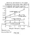
- FIG. 10 is a graph of the resistivity versus weight percent copper for various alternative embodiment metallurgies of the subject invention before and after anneal.
- FIG. 1 is a cross-sectional view of the preferred embodiment of an interconnect metallurgy structure according to the subject invention.
- FIG. 1 represents the interconnect structure after being processed through final annealing.
- the interconnect metallurgy is seen to comprise a four-layer structure over an interplanar stud connection (10) surrounded by an insulator 8 to make connection to a device substrate 6.
- the four-layer structure consists of an intermetallic bottom layer 12′ typically 70nm thick and, in a preferred embodiment would comprise TiAl3.
- layer 14 is typically 850nm thick and consists of a composition of 99,5% aluminum and 0,5% copper (aluminum-0,5% copper hereafter).
- layer 14 is a second intermetallic layer 16′ of the same thickness and composition as layer 12′.
- a layer 18 of aluminum-0,5% copper (or pure aluminum) of approximately 10nm to 50nm thick achieves the structure. While this completes the structure for a single interconnect layer according to the subject invention, it should be recognized by those skilled in the art that said layers can then be repeated in a multiple level sequence to complete the interconnect circuit for the devices.
- FIG. 2 shows a planar insulator 8 and contact stud 10 with a Group IVA metal layer 12 sputter deposited thereon.
- the layer 12 is deposited by the following process. After formation of the device contact metallization 10, the semiconductor wafer would be loaded into a sputtering tool which has been pumped to a low pressure. An in- situ sputter clean is then performed to remove any oxide from the contact metal 10 formation on the wafer at this time.
- This in-situ sputter clean typically is a mild sputter clean, run, for example, at about five minutes at low power (approximately 1000 watt) in a high-pressure argon ambient.
- the first level of metallization 12 is then deposited.
- This first level metallization 12 is comprised of a Group IVA metal, preferably titanium, deposited on the device contact metallization 10 of the wafer in a blanket formation.
- This layer 12 is deposited at low power in a high pressure, high purity, argon plasma from an ultra-pure titanium target at a rate of about 6nm per minute.
- the titanium is deposited to a thickness of approximately 25nm.
- the interconnect metallization layer 14 is next blanket deposited.
- the interconnect metallization 14 is preferably aluminum-0,5% copper (approximately 950nm thick).
- the aluminum-copper is deposited at high power using a direct current magnetron in a high purity argon plasma from an ultra-pure pre-alloyed target typically aluminum-0.5 weight percent copper with a deposition rate of about 150nm per minute.
- said aluminum-copper interconnect metallization 14 is then deposited 25nm of a Group IVA metal similar to the previously deposited metal layer 12 discussed above. Deposition, composition and thickness of said layer 16 is identical to the previously deposited layer 12 (FIG. 4).
- the capping layer 18 is preferably comprised of aluminum-0.05% copper deposited in the same manner as the conductor aluminum-0.5% copper layer 14 as discussed above.
- the purpose of this layer is to: 1) prevent over-etch of metal layer 16; 2) limit the amount of light reflection during the subsequent photoresist steps, and 3) to act as a protective layer against corrosion during subsequent processing. Therefore, any layer which would similarly satisfy the requirements of reducing the amount of light reflection and provide protective anodic capping during subsequent processing would be usable for this layer (e.g. pure aluminum).
- a multilayered photoresist (20, 22 and 24) is then applied to pattern this blanket interconnect metallization. Any number of different photoresist techniques can be used. In particular, multilayered photoresists are well suited for this purpose, as well as, single-layered resists.
- a first resist 20 is applied to a thickness of approximately 1.8 ⁇ m.
- this resist is a diazo-quinone novolak photoresist.
- the resist 20 is baked in an oven in a nitrogen ambient at about 200°C for 30 minutes.
- This resist 20 serves as a sacrificial layer during subsequent metal reactive ion etching (RIE).
- RIE metal reactive ion etching
- a silylating agent 22 such as, HMDS (hexamethyldisilizane).
- HMDS 22 serves as a barrier to the oxygen reactive ion etching which is used to pattern the imaging layer resist 24.
- imaging layer resist 24 is a diazo-quinone novolak positive photoresist.
- the HMDS 22 and imaging resist layer 24 are then baked on a hot plate for 25 minutes at 85°C.
- the imaging layer resist 24 is then exposed for the specific time required when used in conjunction with a specific exposure tool and associated mask.
- the exposed image is developed using conventional developing for the required time depending on the exposure.
- the wafer is then rinsed and dried and the patterned top imaging layer is UV hardened by exposing it to ultraviolet light for a specific period of time, typically, 5 to 10 minutes.
- the HMDS 22 and resist layer 20 are ready to be removed to expose the metal.
- the HMDS 22 and the resist 20 are removed by reactive ion etching. This is accomplished by loading the wafer into a plasma tool and exposing the wafer to a plasma reactive to the HMDS layer 22 (e.g. CF4) and then to a different plasma (e.g. O2) reactive to resist 20.
- a plasma reactive to the HMDS layer 22 e.g. CF4
- a different plasma e.g. O2 reactive to resist 20.
- the polymer residues of the remains of the HMDS layer 22 and the resist 20 are then removed by dipping in a solution of a conventional cleaning etch solution.
- This reactive ion etching of the HMDS layer 22 and the resist 20 has put a lithographic mask into place for the subsequent reactive ion etching of the underlying blanket metal layers.
- the metallurgy can now be reactively ion etched in a multi-step sequence.
- the first step is to break through any oxides which may exist on the top surface of the metallization.
- most of the metal is removed by reactive ion etching.
- An over etch is, then, performed to insure that all of the metal in the previous step has been etched away.
- a passivation step is performed to prevent any metal corrosion.
- the reactive ion etch is typically performed in a single wafer tool under a low pressure.
- Typical plasma composition, pressure, power and time combinations, for performing the above etches in a step-by-step process can be seen from the following Table I. These compositions, pressures, powers and times should be recognized by those skilled in the art as being designed for a specific tool under specific conditions Any comparable times, compositions, pressure, etc., could be similarly fabricated to insure the etch of the blanket metallization.
- the wafer With the completion of the reactive ion etch, the wafer can then be rinsed and dried.
- the reactive ion etch of the metal removes any of the remaining imaging layer resist 24 and most of the the HMDS layer 22 leaving on the surface of the metal the resist 20.
- This resist 20 can be removed by placing the wafer in an oxygen plasma for approximately 45 minutes. The wafer is then placed in a developer at room temperature for a short period of time to remove any oxides that may have formed in the previous step. The wafer is again rinsed and dried.
- the metallization stack can now be annealed by placing the wafer in an oven at 400°C in forming gas for 1 hour in order to form TiAl3 intermetallic layers 12′ and 16′ on the top and the bottom of the aluminum-copper layer 14 and to allow grain growth to occur in the aluminum-copper layer 14.
- a suitable insulator 26 e.g., planar quartz or plasma-enhanced CVD oxide or an organic insulator such as polyimide
- This insulator 26 can then be planarized and/or patterned for stud connection to the repeating interconnect layers deposited onto the base interconnect layer.
- FIG. 9 is a lifetime (hours) versus weight percent copper graph for the electromigration characteristics of both the above-described sputtered four-layered structure and an alternative sputtered three-layer structure (Al/Cu/refractory metal/Al-Cu), as compared to an evaporated three-layer structure patterned by lift-off and an evaporated four-layer structure, patterned by RIE. From FIG. 9 it can be seen that for all weight percent copper compositions, the sputtered interconnect metallurgies are vastly superior to the evaporated metallurgies.
- Fig. 10 is a graph of the resistivity versus weight percent copper for various alternative embodiment metallurgies of the subject invention.
- the metallurgies have been subjected to a 400°C forming gas anneal wherein the plots have been taken both before and after said anneal. From the plots it can clearly be seen that the resistivity of the 0.5 weight percent copper structures are lower than that of the higher weight percent copper films. Additionally, it can also be seen that the annealed films of the four-layer structure have a lower resistivity than the annealed films of the three-layer structure.
- Table II is a further comparison of the electromigration characteristics of sputtered Al-0.5%Cu metallurgy after annealing with intermetallic formation as compared to various other interconnect metallurgies.
- the solubility of copper and aluminum is known to decrease from 5,65 wt.% at 548°C to 0,25 wt.% at room temperature. Therefore, the 0.5% copper film composition of the subject invention has enough copper without theta phase formation to improve both the mechanical properties and reliability, (e.g., electromigration properties) of the alloy over pure aluminum. Moreover, it is recognized that there is enhanced copper uniformity in the subject films due to the fact that said films were sputtered versus the non-uniformity in copper distribution as can be seen in the evaporated aluminum-copper films. In addition, it is also recognized that evaporation results in the uneven distribution of theta particles in the evaporated films which uneven distribution is known to contribute to the poor mechanical corrosion and electrical properties of the prior art films.
- the superior mechanical and electrical properties of the subject metallurgy is therefore directly attributed to the enhanced copper uniformity in these films as result of the deposition by sputtering. Therefore, an improved sputtered copper interconnect metallurgy has been developed that has enhanced reliability, lower resistivity, is dry etchable, and has a superior corrosion resistance than that metallurgy as presently used in the prior art.
- the preferred sputtered (4-layer) metallurgy exhibits lower resistivity and superior electromigration over a wider range of copper compositions than previous prior art structures.
Description
- This invention relates to a semiconductor device having a metallisation structure for the interconnection of semiconductor components on a substrate and more particularly to a multilayered sputtered interconnect metallurgy structure which structure includes a low percent copper content aluminum/copper conductor.
- Thin narrow interconnections have been used for some years for device interconnection purposes in the semiconductor integrated circuit industry. It is predicted that performance of these devices in the future will be limited by the performance of the device interconnection at the submicron level. At the submicron level, various technical problems are known to occur. While aluminum has been the preferred interconnection metal, as device dimensions are scaled down and current density increases, pure aluminum has been known to be susceptible to the problems of electromigration and hillock growth. To overcome the problems experienced with pure aluminum, aluminum has been alloyed with copper to form aluminum-copper. However, high percentage aluminum-copper (> 2%) is known to be difficult to dry etch and corrodes easily.
- In an effort to improve on the use of aluminum-copper as the interconnection metallurgy, aluminum-copper has been taught to be layered with a refractory metal (i.e., U.S. Patent No. US-A-4,017,890). This patent teaches a method and resulting structure for forming narrow intermetallic stripes which carry high currents on bodies such as semiconductors, integrated circuits etc., wherein the conductive stripe includes aluminum or aluminum-copper with at least one transition metal. While the aluminum-copper and transition metal structure has been known to improve the electromigration problems associated with aluminum-copper, the problems of etching and corrosion, as well as, the complete elimination of hillocks have not been solved.
- As known in the art, hillocks are known to result from the large differences between the thermal expansion coefficients of the metal interconnect lines and the substrate. To eliminate and minimize hillock formation, it has been known in the art to use a multilayered structure instead of a single layer of the interconnect metallurgy. An effective reduction in hillock formation has been found to be achieved by using a multilayered structure of aluminum or aluminum intermetallic with a layer of refractory metal. Wherefore, a typical interconnect metallurgy structure would comprise a layered structure of aluminum silicon compound onto which there has been deposited, a layer of refractory metal, such as, titanium (see article "Homogeneous and Layered Films of Aluminum/Silicon with Titanium For Multilevel Interconnects", 1988 IEEE, V-MIC Conference, June 25-26, 1985).
- There have also been refinements to this layered metal structure to provide a lower resistivity, hillock free, interconnect metallurgy. These refinements include the incorporation of a barrier metal of, for example, titanium tungsten or titanium nitride under the aluminum silicon to prevent contact spiking and prevent the formation of ternary compounds in the aluminum silicon alloy (see article "Multilayerd Interconnections For VLSI" MRS Symposia Proceedings, Fall, 1987).
- In addition, in this area, there have also been other proposed device interconnect structures to reduce resistivity and provide a more planar and defect free interconnect structure.
- For example, IBM Technical Disclosure Bulletin, Vol. 21, No. 11, April, 1979, pp. 4527-4528, teaches the enhancement of the metallurgy for the interconnection due to sputtered deposition. Moreover, the feature of using a capping layer to improve performance has been proposed in IBM TDB Vol. 17, No. 1A, 1984 and TDB Vol. 21, No. 2, July 1978. However, no structure has been discovered which can satisfy all performance criteria providing a low resistance, hillock free, corrosion resistant, etchable, interconnection metallurgy structure.
- It is, therefore, an object of the present invention to provide sputtered low weight percent copper (< 2%) content aluminum/copper conductor for device interconnection on a substrate with superior electromigration characteristics.
- It is a still further object of the present invention to develop a multilayered interconnect metallurgy structure that is hillock free, dry etchable and corrosion resistant.
- It is another object of the present invention to provide a multilayered interconnect metallurgy structure which has a low resistivity.
- A semiconductor device having a sputtered low-copper concentration multilayered, component interconnect metallurgy structure is set out in
Claim 1, a method of forming such a device is set out inClaim 5. The interconnect metallization structure comprises a sputtered aluminum-copper (<2%) weight percent copper conductor. In the preferred embodiment, the conductor layer is formed with a top and bottom layer of an intermetallic, said intermetallic also being sputtered and being of a thickness of approximately 70nm. Onto said intermetallic layer is further deposited an etch stop, and non-corrosive, protective capping layer. - FIG. 1 is a cross-sectional view of the preferred embodiment of an interconnect metallurgy according to the subject invention.
- FIGS. 2 through 8 are cross-sectional views of the process for building the preferred interconnect metallurgy of the subject invention in a step-by-step fashion.
- FIG. 9 is a graph of the lifetime (hours) versus weight percent copper for interconnect metalluries of the subject invention as compared to prior art interconnect metallizations.
- FIG. 10 is a graph of the resistivity versus weight percent copper for various alternative embodiment metallurgies of the subject invention before and after anneal.
- FIG. 1 is a cross-sectional view of the preferred embodiment of an interconnect metallurgy structure according to the subject invention. FIG. 1 represents the interconnect structure after being processed through final annealing.
- Referring to FIG. 1, the interconnect metallurgy is seen to comprise a four-layer structure over an interplanar stud connection (10) surrounded by an
insulator 8 to make connection to adevice substrate 6. The four-layer structure consists of anintermetallic bottom layer 12′ typically 70nm thick and, in a preferred embodiment would comprise TiAl₃. - Above is a low percent (< 2%) weight percent copper, aluminum-copper,
conductor layer 14. At the end of the process,layer 14 is typically 850nm thick and consists of a composition of 99,5% aluminum and 0,5% copper (aluminum-0,5% copper hereafter). Onlayer 14 is a secondintermetallic layer 16′ of the same thickness and composition aslayer 12′. Finally, alayer 18 of aluminum-0,5% copper (or pure aluminum) of approximately 10nm to 50nm thick achieves the structure. While this completes the structure for a single interconnect layer according to the subject invention, it should be recognized by those skilled in the art that said layers can then be repeated in a multiple level sequence to complete the interconnect circuit for the devices. - Referring now to FIG. 2, FIG. 2 shows a
planar insulator 8 and contactstud 10 with a GroupIVA metal layer 12 sputter deposited thereon. Thelayer 12 is deposited by the following process. After formation of thedevice contact metallization 10, the semiconductor wafer would be loaded into a sputtering tool which has been pumped to a low pressure. An in- situ sputter clean is then performed to remove any oxide from thecontact metal 10 formation on the wafer at this time. This in-situ sputter clean typically is a mild sputter clean, run, for example, at about five minutes at low power (approximately 1000 watt) in a high-pressure argon ambient. - Following the sputter cleaning, the first level of
metallization 12 is then deposited. Thisfirst level metallization 12 is comprised of a Group IVA metal, preferably titanium, deposited on thedevice contact metallization 10 of the wafer in a blanket formation. Thislayer 12 is deposited at low power in a high pressure, high purity, argon plasma from an ultra-pure titanium target at a rate of about 6nm per minute. Preferably, the titanium is deposited to a thickness of approximately 25nm. Referring now to FIG. 3, following the deposition of thelayer 12, theinterconnect metallization layer 14 is next blanket deposited. Theinterconnect metallization 14 is preferably aluminum-0,5% copper (approximately 950nm thick). The aluminum-copper is deposited at high power using a direct current magnetron in a high purity argon plasma from an ultra-pure pre-alloyed target typically aluminum-0.5 weight percent copper with a deposition rate of about 150nm per minute. - Onto said aluminum-
copper interconnect metallization 14 is then deposited 25nm of a Group IVA metal similar to the previously depositedmetal layer 12 discussed above. Deposition, composition and thickness of saidlayer 16 is identical to the previously deposited layer 12 (FIG. 4). - From FIG. 5, onto said
metal layer 16 is then blanket deposited asuitable capping layer 18 to complete the interconnect metallurgy at this level. Thecapping layer 18 is preferably comprised of aluminum-0.05% copper deposited in the same manner as the conductor aluminum-0.5%copper layer 14 as discussed above. The purpose of this layer is to: 1) prevent over-etch ofmetal layer 16; 2) limit the amount of light reflection during the subsequent photoresist steps, and 3) to act as a protective layer against corrosion during subsequent processing. Therefore, any layer which would similarly satisfy the requirements of reducing the amount of light reflection and provide protective anodic capping during subsequent processing would be usable for this layer (e.g. pure aluminum). - Referring now to FIG. 6, on top of
metallization 18, a multilayered photoresist (20, 22 and 24) is then applied to pattern this blanket interconnect metallization. Any number of different photoresist techniques can be used. In particular, multilayered photoresists are well suited for this purpose, as well as, single-layered resists. - With a multilayered resist as shown in FIG. 6, a
first resist 20 is applied to a thickness of approximately 1.8 µm. In the preferred embodiment this resist is a diazo-quinone novolak photoresist. Theresist 20 is baked in an oven in a nitrogen ambient at about 200°C for 30 minutes. This resist 20 serves as a sacrificial layer during subsequent metal reactive ion etching (RIE). - Onto said resist 20 is then deposited 20nm of a
silylating agent 22, such as, HMDS (hexamethyldisilizane). TheHMDS 22 serves as a barrier to the oxygen reactive ion etching which is used to pattern the imaging layer resist 24. - Onto said
HMDS layer 22 is next deposited an imaging layer resist 24 to a thickness of about 0.9-1.2 micrometers. Similar to resist 20, imaging resist 24 is a diazo-quinone novolak positive photoresist. TheHMDS 22 and imaging resistlayer 24 are then baked on a hot plate for 25 minutes at 85°C.
The imaging layer resist 24 is then exposed for the specific time required when used in conjunction with a specific exposure tool and associated mask. The exposed image is developed using conventional developing for the required time depending on the exposure. The wafer is then rinsed and dried and the patterned top imaging layer is UV hardened by exposing it to ultraviolet light for a specific period of time, typically, 5 to 10 minutes. - Following the patterning of the top imaging resist 24, the
HMDS 22 and resistlayer 20 are ready to be removed to expose the metal. TheHMDS 22 and the resist 20 are removed by reactive ion etching. This is accomplished by loading the wafer into a plasma tool and exposing the wafer to a plasma reactive to the HMDS layer 22 (e.g. CF₄) and then to a different plasma (e.g. O₂) reactive to resist 20. The polymer residues of the remains of theHMDS layer 22 and the resist 20 are then removed by dipping in a solution of a conventional cleaning etch solution. This reactive ion etching of theHMDS layer 22 and the resist 20, has put a lithographic mask into place for the subsequent reactive ion etching of the underlying blanket metal layers. - The metallurgy can now be reactively ion etched in a multi-step sequence. The first step is to break through any oxides which may exist on the top surface of the metallization. Next, most of the metal is removed by reactive ion etching. An over etch is, then, performed to insure that all of the metal in the previous step has been etched away. Finally, a passivation step is performed to prevent any metal corrosion.
- The reactive ion etch is typically performed in a single wafer tool under a low pressure. Typical plasma composition, pressure, power and time combinations, for performing the above etches in a step-by-step process can be seen from the following Table I. These compositions, pressures, powers and times should be recognized by those skilled in the art as being designed for a specific tool under specific conditions Any comparable times, compositions, pressure, etc., could be similarly fabricated to insure the etch of the blanket metallization.

- With the completion of the reactive ion etch, the wafer can then be rinsed and dried.
- Referring now to FIG. 7, it can be seen that the reactive ion etch of the metal removes any of the remaining imaging layer resist 24 and most of the the
HMDS layer 22 leaving on the surface of the metal the resist 20. This resist 20 can be removed by placing the wafer in an oxygen plasma for approximately 45 minutes. The wafer is then placed in a developer at room temperature for a short period of time to remove any oxides that may have formed in the previous step. The wafer is again rinsed and dried. - With removal of this final layer of the resist 20, the metallization stack can now be annealed by placing the wafer in an oven at 400°C in forming gas for 1 hour in order to form TiAl₃ intermetallic layers 12′ and 16′ on the top and the bottom of the aluminum-
copper layer 14 and to allow grain growth to occur in the aluminum-copper layer 14. - From FIG. 8, it can be seen that once the metallization stack has been annealed (to the structure of FIG. 1) a suitable insulator 26 (e.g., planar quartz or plasma-enhanced CVD oxide or an organic insulator such as polyimide) can be blanket deposited over the multilayered interconnect structure. This
insulator 26 can then be planarized and/or patterned for stud connection to the repeating interconnect layers deposited onto the base interconnect layer. - The superior performance of the interconnect metallurgy of the subject invention over that which is known in the prior art can be seen in the following figures. FIG. 9 is a lifetime (hours) versus weight percent copper graph for the electromigration characteristics of both the above-described sputtered four-layered structure and an alternative sputtered three-layer structure (Al/Cu/refractory metal/Al-Cu), as compared to an evaporated three-layer structure patterned by lift-off and an evaporated four-layer structure, patterned by RIE. From FIG. 9 it can be seen that for all weight percent copper compositions, the sputtered interconnect metallurgies are vastly superior to the evaporated metallurgies.
- Fig. 10 is a graph of the resistivity versus weight percent copper for various alternative embodiment metallurgies of the subject invention. The metallurgies have been subjected to a 400°C forming gas anneal wherein the plots have been taken both before and after said anneal. From the plots it can clearly be seen that the resistivity of the 0.5 weight percent copper structures are lower than that of the higher weight percent copper films. Additionally, it can also be seen that the annealed films of the four-layer structure have a lower resistivity than the annealed films of the three-layer structure.
- The following Table II is a further comparison of the electromigration characteristics of sputtered Al-0.5%Cu metallurgy after annealing with intermetallic formation as compared to various other interconnect metallurgies.


- From the table it can be seen that the sputtered 0,5% copper metallurgy provides the longest electromigration capability with the lowest resistivity.
- In general, while the corrosion resistance of bulk aluminum is greatly decreased by the addition of copper, it is known and recognized in the art: (see, for example, J. Zahavi, M. Rotel, H.C.W. Huang, P.A. Totta, "Corrosion behavior of Al-Cu Alloy Thin Films in Microelectronics." Proceedings of International Congress of Metallic Corrosion. Toronto, June, 1984.) that the corrosion resistance of reactive ion etched low copper containing films of aluminum (e.g., less than 1% copper) are at least as good as bulk aluminum. This is in contradiction to that skill in the art which recognizes that the corrosion resistance of higher percentage (above 1%) copper-aluminum films significantly degrades below that of pure aluminum. While detailed understanding of the mechanism of the performance of the subject interconnect metallurgy is not known, several principles have been extended by the inventors to explain the superior electromigration and resistivity results as seen above.
- The solubility of copper and aluminum is known to decrease from 5,65 wt.% at 548°C to 0,25 wt.% at room temperature. Therefore, the 0.5% copper film composition of the subject invention has enough copper without theta phase formation to improve both the mechanical properties and reliability, (e.g., electromigration properties) of the alloy over pure aluminum. Moreover, it is recognized that there is enhanced copper uniformity in the subject films due to the fact that said films were sputtered versus the non-uniformity in copper distribution as can be seen in the evaporated aluminum-copper films. In addition, it is also recognized that evaporation results in the uneven distribution of theta particles in the evaporated films which uneven distribution is known to contribute to the poor mechanical corrosion and electrical properties of the prior art films. The superior mechanical and electrical properties of the subject metallurgy is therefore directly attributed to the enhanced copper uniformity in these films as result of the deposition by sputtering. Therefore, an improved sputtered copper interconnect metallurgy has been developed that has enhanced reliability, lower resistivity, is dry etchable, and has a superior corrosion resistance than that metallurgy as presently used in the prior art. The preferred sputtered (4-layer) metallurgy exhibits lower resistivity and superior electromigration over a wider range of copper compositions than previous prior art structures.
Claims (5)
- A semiconductor device including a substrate and a metallization structure for the interconnection of semiconductor components on said substrate said metallization structure comprising:a) a layer (14) of sputter deposited aluminum-copper of greater than 0% and less than 2% copper by weight; andb) an intermetallic layer (16) formed at the surface of said aluminum-copper layer, said intermetallic layer formed of a sputter-deposited metal selected from the group including titanium, zirconium and hafnium, and aluminum of said aluminum-copper layer.
- The semiconductor device of Claim 1 further comprising:
c) an intermetallic layer (12) formed between said substrate and said layer a) (14) of sputter deposited aluminum-copper, said intermetallic layer formed of a sputter-deposited metal selected from the group including titanium, zirconium and hafnium, and aluminum of said aluminum-copper layer. - The semiconductor device of claim 2 further comprising:
d) a metal overlayer (18) deposited on layer (b) (16). - The semiconductor device of Claim 3 wherein said metal overlayer d) (18) is aluminum-copper alloy containing greater than 0% to less than 2% copper by weight.
- A method of forming a semiconductor device including a substrate and a metallization structure for connecting semiconductor components on said substrate, said method comprising the steps of:a) sputter depositing a first layer (12) of at least one of the metals selected from the group including titanium, zirconium and hafnium onto said substrate,b) sputter depositing onto said first layer a second layer (14) of aluminum copper of greater than 0% and less than 2% copper by weight,c) sputter depositing a third layer (16) of the same metal as in step a, andd) annealing the structure to form an intermetallic of the selected metal and aluminum.
Applications Claiming Priority (2)
| Application Number | Priority Date | Filing Date | Title |
|---|---|---|---|
| US07/339,533 US5071714A (en) | 1989-04-17 | 1989-04-17 | Multilayered intermetallic connection for semiconductor devices |
| US339533 | 1989-04-17 |
Publications (3)
| Publication Number | Publication Date |
|---|---|
| EP0395560A2 EP0395560A2 (en) | 1990-10-31 |
| EP0395560A3 EP0395560A3 (en) | 1991-01-02 |
| EP0395560B1 true EP0395560B1 (en) | 1994-11-17 |
Family
ID=23329454
Family Applications (1)
| Application Number | Title | Priority Date | Filing Date |
|---|---|---|---|
| EP90480044A Expired - Lifetime EP0395560B1 (en) | 1989-04-17 | 1990-03-13 | Multilayered intermetallic connection for semiconductor devices |
Country Status (5)
| Country | Link |
|---|---|
| US (1) | US5071714A (en) |
| EP (1) | EP0395560B1 (en) |
| JP (1) | JPH0752733B2 (en) |
| CA (1) | CA2009247A1 (en) |
| DE (1) | DE69014149T2 (en) |
Families Citing this family (66)
| Publication number | Priority date | Publication date | Assignee | Title |
|---|---|---|---|---|
| JP2811131B2 (en) * | 1991-04-26 | 1998-10-15 | 三菱電機株式会社 | Wiring connection structure of semiconductor device and method of manufacturing the same |
| US5606203A (en) * | 1993-01-20 | 1997-02-25 | Kabushiki Kaisha Toshiba | Semiconductor device having Al-Cu wiring lines where Cu concentration is related to line width |
| US5635763A (en) * | 1993-03-22 | 1997-06-03 | Sanyo Electric Co., Ltd. | Semiconductor device having cap-metal layer |
| JP3256623B2 (en) * | 1993-05-28 | 2002-02-12 | 株式会社東芝 | Method for manufacturing semiconductor device |
| US5360995A (en) * | 1993-09-14 | 1994-11-01 | Texas Instruments Incorporated | Buffered capped interconnect for a semiconductor device |
| JP3379049B2 (en) * | 1993-10-27 | 2003-02-17 | 富士通株式会社 | Surface acoustic wave device and method of manufacturing the same |
| US5488013A (en) * | 1993-12-20 | 1996-01-30 | International Business Machines Corporation | Method of forming transverse diffusion barrier interconnect structure |
| US5518805A (en) * | 1994-04-28 | 1996-05-21 | Xerox Corporation | Hillock-free multilayer metal lines for high performance thin film structures |
| US5565707A (en) * | 1994-10-31 | 1996-10-15 | International Business Machines Corporation | Interconnect structure using a Al2 Cu for an integrated circuit chip |
| US6285082B1 (en) * | 1995-01-03 | 2001-09-04 | International Business Machines Corporation | Soft metal conductor |
| JPH09115829A (en) * | 1995-10-17 | 1997-05-02 | Nissan Motor Co Ltd | Semiconductor device with aluminium wiring part and method of manufacturing |
| KR0186206B1 (en) * | 1995-11-21 | 1999-05-01 | 구자홍 | Liquid crystal display element and its manufacturing method |
| GB2323475B (en) * | 1995-11-21 | 1999-08-11 | Lg Electronics Inc | Controlling the generation of hillocks in liquid crystal devices |
| US5582881A (en) * | 1996-02-16 | 1996-12-10 | Advanced Micro Devices, Inc. | Process for deposition of a Ti/TiN cap layer on aluminum metallization and apparatus |
| US5918149A (en) * | 1996-02-16 | 1999-06-29 | Advanced Micro Devices, Inc. | Deposition of a conductor in a via hole or trench |
| KR100270593B1 (en) * | 1996-06-11 | 2000-12-01 | 포만 제프리 엘 | Partially-overlapped interconnect structure and method of making |
| US6309971B1 (en) | 1996-08-01 | 2001-10-30 | Cypress Semiconductor Corporation | Hot metallization process |
| US5956573A (en) * | 1997-01-17 | 1999-09-21 | International Business Machines Corporation | Use of argon sputtering to modify surface properties by thin film deposition |
| US5943601A (en) * | 1997-04-30 | 1999-08-24 | International Business Machines Corporation | Process for fabricating a metallization structure |
| US6130161A (en) * | 1997-05-30 | 2000-10-10 | International Business Machines Corporation | Method of forming copper interconnections with enhanced electromigration resistance and reduced defect sensitivity |
| EP0895278A3 (en) * | 1997-08-01 | 2000-08-23 | Siemens Aktiengesellschaft | Patterning process |
| JP3500308B2 (en) | 1997-08-13 | 2004-02-23 | インターナショナル・ビジネス・マシーンズ・コーポレーション | Integrated circuit |
| US6140236A (en) * | 1998-04-21 | 2000-10-31 | Kabushiki Kaisha Toshiba | High throughput A1-Cu thin film sputtering process on small contact via for manufacturable beol wiring |
| JP3322305B2 (en) * | 1999-02-25 | 2002-09-09 | 日本電気株式会社 | Method for manufacturing semiconductor device |
| US6344281B1 (en) * | 1999-10-18 | 2002-02-05 | Cypress Semiconductor Corporation | Aluminum metallization method and product |
| US6413863B1 (en) * | 2000-01-24 | 2002-07-02 | Taiwan Semiconductor Manufacturing Company | Method to resolve the passivation surface roughness during formation of the AlCu pad for the copper process |
| US6613671B1 (en) * | 2000-03-03 | 2003-09-02 | Micron Technology, Inc. | Conductive connection forming methods, oxidation reducing methods, and integrated circuits formed thereby |
| DE10053915C2 (en) * | 2000-10-31 | 2002-11-14 | Infineon Technologies Ag | Manufacturing process for an integrated circuit |
| JP3445971B2 (en) * | 2000-12-14 | 2003-09-16 | 富士通株式会社 | Surface acoustic wave device |
| US20060252265A1 (en) * | 2002-03-06 | 2006-11-09 | Guangxiang Jin | Etching high-kappa dielectric materials with good high-kappa foot control and silicon recess control |
| US6806095B2 (en) | 2002-03-06 | 2004-10-19 | Padmapani C. Nallan | Method of plasma etching of high-K dielectric materials with high selectivity to underlying layers |
| US7094704B2 (en) * | 2002-05-09 | 2006-08-22 | Applied Materials, Inc. | Method of plasma etching of high-K dielectric materials |
| US6902681B2 (en) * | 2002-06-26 | 2005-06-07 | Applied Materials Inc | Method for plasma etching of high-K dielectric materials |
| US6855643B2 (en) * | 2002-07-12 | 2005-02-15 | Padmapani C. Nallan | Method for fabricating a gate structure |
| US20040007561A1 (en) * | 2002-07-12 | 2004-01-15 | Applied Materials, Inc. | Method for plasma etching of high-K dielectric materials |
| US6960306B2 (en) * | 2002-07-31 | 2005-11-01 | Infineon Technologies Ag | Low Cu percentages for reducing shorts in AlCu lines |
| JP2005268454A (en) * | 2004-03-17 | 2005-09-29 | Nec Electronics Corp | Semiconductor apparatus and manufacturing method therefor |
| US20060102197A1 (en) * | 2004-11-16 | 2006-05-18 | Kang-Lie Chiang | Post-etch treatment to remove residues |
| US20070202700A1 (en) * | 2006-02-27 | 2007-08-30 | Applied Materials, Inc. | Etch methods to form anisotropic features for high aspect ratio applications |
| US7368394B2 (en) * | 2006-02-27 | 2008-05-06 | Applied Materials, Inc. | Etch methods to form anisotropic features for high aspect ratio applications |
| US7655571B2 (en) * | 2006-10-26 | 2010-02-02 | Applied Materials, Inc. | Integrated method and apparatus for efficient removal of halogen residues from etched substrates |
| US7846845B2 (en) * | 2006-10-26 | 2010-12-07 | Applied Materials, Inc. | Integrated method for removal of halogen residues from etched substrates in a processing system |
| US7946759B2 (en) * | 2007-02-16 | 2011-05-24 | Applied Materials, Inc. | Substrate temperature measurement by infrared transmission |
| US20080203056A1 (en) * | 2007-02-26 | 2008-08-28 | Judy Wang | Methods for etching high aspect ratio features |
| JP2009021584A (en) * | 2007-06-27 | 2009-01-29 | Applied Materials Inc | High temperature etching method of high k material gate structure |
| US20100330805A1 (en) * | 2007-11-02 | 2010-12-30 | Kenny Linh Doan | Methods for forming high aspect ratio features on a substrate |
| JP6054314B2 (en) | 2011-03-01 | 2016-12-27 | アプライド マテリアルズ インコーポレイテッドApplied Materials,Incorporated | Method and apparatus for substrate transport and radical confinement |
| US8992689B2 (en) | 2011-03-01 | 2015-03-31 | Applied Materials, Inc. | Method for removing halogen-containing residues from substrate |
| US11171008B2 (en) | 2011-03-01 | 2021-11-09 | Applied Materials, Inc. | Abatement and strip process chamber in a dual load lock configuration |
| CN103403852B (en) | 2011-03-01 | 2016-06-08 | 应用材料公司 | The elimination of double; two load locks configuration and lift-off processing chamber |
| US8845816B2 (en) | 2011-03-01 | 2014-09-30 | Applied Materials, Inc. | Method extending the service interval of a gas distribution plate |
| US9533332B2 (en) | 2011-10-06 | 2017-01-03 | Applied Materials, Inc. | Methods for in-situ chamber clean utilized in an etching processing chamber |
| KR102068186B1 (en) | 2012-02-29 | 2020-02-11 | 어플라이드 머티어리얼스, 인코포레이티드 | Abatement and strip process chamber in a load lock configuration |
| US8932947B1 (en) | 2013-07-23 | 2015-01-13 | Applied Materials, Inc. | Methods for forming a round bottom silicon trench recess for semiconductor applications |
| US9214377B2 (en) | 2013-10-31 | 2015-12-15 | Applied Materials, Inc. | Methods for silicon recess structures in a substrate by utilizing a doping layer |
| JP6455335B2 (en) * | 2015-06-23 | 2019-01-23 | 三菱電機株式会社 | Semiconductor device |
| US9831194B1 (en) | 2016-07-06 | 2017-11-28 | Globalfoundries Inc. | Edge compression layers |
| US10641726B2 (en) | 2017-02-01 | 2020-05-05 | Seagate Technology Llc | Fabrication of a nanochannel for DNA sequencing using electrical plating to achieve tunneling electrode gap |
| US10640827B2 (en) * | 2017-02-01 | 2020-05-05 | Seagate Technology Llc | Fabrication of wedge shaped electrode for enhanced DNA sequencing using tunneling current |
| US10889857B2 (en) | 2017-02-01 | 2021-01-12 | Seagate Technology Llc | Method to fabricate a nanochannel for DNA sequencing based on narrow trench patterning process |
| US10731210B2 (en) | 2017-02-01 | 2020-08-04 | Seagate Technology Llc | Fabrication of nanochannel with integrated electrodes for DNA sequencing using tunneling current |
| US10761058B2 (en) | 2017-02-01 | 2020-09-01 | Seagate Technology Llc | Nanostructures to control DNA strand orientation and position location for transverse DNA sequencing |
| US20180259475A1 (en) | 2017-03-09 | 2018-09-13 | Seagate Technology Llc | Vertical nanopore coupled with a pair of transverse electrodes having a uniform ultrasmall nanogap for dna sequencing |
| US10752947B2 (en) | 2017-03-09 | 2020-08-25 | Seagate Technology Llc | Method to amplify transverse tunneling current discrimination of DNA nucleotides via nucleotide site specific attachment of dye-peptide |
| US10964653B2 (en) | 2017-09-28 | 2021-03-30 | Taiwan Semiconductor Manufacturing Co., Ltd. | Method of forming a semiconductor device comprising top conductive pads |
| CN113675344B (en) * | 2021-08-20 | 2023-09-05 | 电子科技大学 | Metal electrode material for organic photoelectric detector and preparation method thereof |
Family Cites Families (5)
| Publication number | Priority date | Publication date | Assignee | Title |
|---|---|---|---|---|
| US4017890A (en) * | 1975-10-24 | 1977-04-12 | International Business Machines Corporation | Intermetallic compound layer in thin films for improved electromigration resistance |
| JPS5951747B2 (en) * | 1979-12-07 | 1984-12-15 | 株式会社日立製作所 | Micro wiring structure |
| US4612257A (en) * | 1983-05-02 | 1986-09-16 | Signetics Corporation | Electrical interconnection for semiconductor integrated circuits |
| US4673623A (en) * | 1985-05-06 | 1987-06-16 | The Board Of Trustees Of The Leland Stanford Junior University | Layered and homogeneous films of aluminum and aluminum/silicon with titanium and tungsten for multilevel interconnects |
| EP0307272A3 (en) * | 1987-09-09 | 1989-07-12 | STMicroelectronics, Inc. | Aluminum alloy semiconductor interconnections having high purity titanium or niobium barrier layer |
-
1989
- 1989-04-17 US US07/339,533 patent/US5071714A/en not_active Expired - Lifetime
-
1990
- 1990-02-02 CA CA2009247A patent/CA2009247A1/en active Granted
- 1990-03-13 DE DE69014149T patent/DE69014149T2/en not_active Expired - Lifetime
- 1990-03-13 EP EP90480044A patent/EP0395560B1/en not_active Expired - Lifetime
- 1990-04-16 JP JP2097818A patent/JPH0752733B2/en not_active Expired - Lifetime
Non-Patent Citations (1)
| Title |
|---|
| IBM TECHNICAL DISCLOSURE BULLETIN, vol. 21, no. 11, April 1979, NEW YORK, US, pp. 4527-4528 ; P.S. HOE and J.K. HOWARD : "Sputtered metallurgy process for electromigration improvement of A1-Cu interconnections" * |
Also Published As
| Publication number | Publication date |
|---|---|
| US5071714A (en) | 1991-12-10 |
| EP0395560A2 (en) | 1990-10-31 |
| CA2009247A1 (en) | 1990-10-17 |
| DE69014149D1 (en) | 1994-12-22 |
| JPH02296334A (en) | 1990-12-06 |
| JPH0752733B2 (en) | 1995-06-05 |
| EP0395560A3 (en) | 1991-01-02 |
| DE69014149T2 (en) | 1995-05-24 |
Similar Documents
| Publication | Publication Date | Title |
|---|---|---|
| EP0395560B1 (en) | Multilayered intermetallic connection for semiconductor devices | |
| CA2009247C (en) | Multilayered intermetallic connection for semiconductor devices | |
| US5920794A (en) | Electromigration resistant metallization process microcircuit interconnections with RF-reactively sputtered titanium tungsten and gold | |
| US4087314A (en) | Bonding pedestals for semiconductor devices | |
| US6255733B1 (en) | Metal-alloy interconnections for integrated circuits | |
| US5994217A (en) | Post metallization stress relief annealing heat treatment for ARC TiN over aluminum layers | |
| US5231053A (en) | Process of forming a tri-layer titanium coating for an aluminum layer of a semiconductor device | |
| US5171642A (en) | Multilayered intermetallic connection for semiconductor devices | |
| US5943601A (en) | Process for fabricating a metallization structure | |
| EP0030633A1 (en) | Nickel-gold-nickel conductors for solid state devices | |
| US5288951A (en) | Copper-based metallizations for hybrid integrated circuits | |
| US6174798B1 (en) | Process for forming metal interconnect stack for integrated circuit structure | |
| JP3236225B2 (en) | Semiconductor device and manufacturing method thereof | |
| US5909635A (en) | Cladding of an interconnect for improved electromigration performance | |
| US7560369B2 (en) | Method of forming metal line in semiconductor device | |
| US5248384A (en) | Rapid thermal treatment to eliminate metal void formation in VLSI manufacturing process | |
| US5290733A (en) | Method of manufacturing semiconductor devices including depositing aluminum on aluminum leads | |
| EP0875923A2 (en) | Multilayer metallization structure comprising a group IVA metal | |
| JP3249196B2 (en) | Method for manufacturing semiconductor device | |
| US6960306B2 (en) | Low Cu percentages for reducing shorts in AlCu lines | |
| EP0348119B1 (en) | Method of processing metal connectors on semi-conductor devices | |
| JPH10308362A (en) | Metallization structure | |
| JP3510943B2 (en) | Method for manufacturing semiconductor device | |
| JPH05182937A (en) | Dry-etching method | |
| JPH05102098A (en) | Wiring forming method |
Legal Events
| Date | Code | Title | Description |
|---|---|---|---|
| PUAI | Public reference made under article 153(3) epc to a published international application that has entered the european phase |
Free format text: ORIGINAL CODE: 0009012 |
|
| AK | Designated contracting states |
Kind code of ref document: A2 Designated state(s): DE FR GB |
|
| PUAL | Search report despatched |
Free format text: ORIGINAL CODE: 0009013 |
|
| AK | Designated contracting states |
Kind code of ref document: A3 Designated state(s): DE FR GB |
|
| 17P | Request for examination filed |
Effective date: 19901213 |
|
| 17Q | First examination report despatched |
Effective date: 19930305 |
|
| GRAA | (expected) grant |
Free format text: ORIGINAL CODE: 0009210 |
|
| AK | Designated contracting states |
Kind code of ref document: B1 Designated state(s): DE FR GB |
|
| REF | Corresponds to: |
Ref document number: 69014149 Country of ref document: DE Date of ref document: 19941222 |
|
| ET | Fr: translation filed | ||
| PLBE | No opposition filed within time limit |
Free format text: ORIGINAL CODE: 0009261 |
|
| STAA | Information on the status of an ep patent application or granted ep patent |
Free format text: STATUS: NO OPPOSITION FILED WITHIN TIME LIMIT |
|
| 26N | No opposition filed | ||
| REG | Reference to a national code |
Ref country code: GB Ref legal event code: IF02 |
|
| REG | Reference to a national code |
Ref country code: GB Ref legal event code: 746 Effective date: 20090216 |
|
| PGFP | Annual fee paid to national office [announced via postgrant information from national office to epo] |
Ref country code: GB Payment date: 20090320 Year of fee payment: 20 |
|
| PGFP | Annual fee paid to national office [announced via postgrant information from national office to epo] |
Ref country code: DE Payment date: 20090406 Year of fee payment: 20 |
|
| PGFP | Annual fee paid to national office [announced via postgrant information from national office to epo] |
Ref country code: FR Payment date: 20090310 Year of fee payment: 20 |
|
| REG | Reference to a national code |
Ref country code: GB Ref legal event code: PE20 Expiry date: 20100312 |
|
| PG25 | Lapsed in a contracting state [announced via postgrant information from national office to epo] |
Ref country code: GB Free format text: LAPSE BECAUSE OF EXPIRATION OF PROTECTION Effective date: 20100312 |
|
| PG25 | Lapsed in a contracting state [announced via postgrant information from national office to epo] |
Ref country code: DE Free format text: LAPSE BECAUSE OF EXPIRATION OF PROTECTION Effective date: 20100313 |